Effect of Annealing on Optical and Photo Conducting
Properties of ZnO Thin Films by Spin Coating
RAJESH, S.1, GANESH. T2 and FRANCIS P. XAVIER3
1
PG & Research Department of Physics, A. M. Jain College, Chennai -600 114. India
2
PG & Research Department of Physics, Presidency College, Chennai – 600 005. India
3
Loyola Institute of Frontier Energy, Physics Department, Loyola College, Chennai 600 034, India
ABSTRACT
ZnO thin films were prepared by sol-gel process using spin coating technique. The precursor solution was prepared using Zinc acetate dihydrate, monoethanolamine and 2-methoxy ethanol. The ZnO films were deposited on microscopic glass substrates and post annealed at four different temperatures 623K, 723K, 773K and 823K. The optical property was characterized using UV-Vis Spectrophotometer. The surface morphology of the film was evaluated by Scanning Electron Microscope (SEM). The films were subjected for FT-IR studies, the absorption and transmission were found using FT-IR spectrometer.The transmittance for the annealed film at 773K showed least transmittance and maximum absorbance of the four films. Conductivity measurements were carried out for all the films. Electrical conductivity for the 773K annealed film showed maximum conductivity. The photo response was maximum for film annealed at 773K. Temperature dependent conductivity showed lowest activation energy for film annealed at 773K.
Keywords: Zinc oxide, thin films, sol-gel, optical and electrical properties.
1. INTRODUCTION
Zinc oxide (ZnO) thin films are one of the most prominent transparent conducting oxides. The properties of zinc oxide (ZnO) are currently subject of
promising metal oxide semi-conductor ZnO has received considerable attention in the recent years. ZnO usually exhibits n-type conductivity with a direct optical energy gap of 3.3 eV which is large enough to transmit most of the useful solar radiation.
Several techniques have been used to prepare ZnO such as pulsed laser deposition (PLD)1, molecular beam epitaxy (MBE)2, DC Magnetron sputtering3, metal organic chemical vapour deposition (MOCVD)4,5, spray pyrolysis6-8, hybrid beam deposition(HBD)9 and sol-gel technique10. Sol-gel process is known to have the distinct advantage of simple process and easy control of the film composition especially uniform thickness. Thin films of undoped ZnO were prepared on glass substrate at different post annealed temperatures. UV-Visible measurements for transmittance and absorption have been carried using Varian Cary 5E spectrometer. Scanning Electron microscope (SEM) measurements were performed to characterize the surface morphology, using FEI quanta FEG HR-SEM. Conductivity and temperature dependent conductivity studies were carried out to understand the electrical properties. FT-IR was recorded using PE FTIR in order to establish the inter-atomic bonding that enables effective conductivity. In this paper we report sol –gel technique to prepare zinc oxide annealed thin film for effective photo conducting by spin-coating.
2. MATERIALS AND METHODS (Experimental Details)
In this study undoped ZnO thin films were prepared by sol gel and spin coating methods on glass substrates. The pre cursor solution of undoped ZnO was
prepared by sol gel method using Zinc acetate dihydrate, monoethanolamine (MEA) and 2-methoxy ethanol. All the chemicals were used as purchased without any purification. Zinc acetate dihydrate was first dissolved in a mixture of 2-methoxy ethanol and monoethanolamine at room temperature. The concentration of zinc acetate was 0.5mol/litre and the molar ratio of monoethanolamine to zinc acetate was kept as 1:1. A homogenous and clear solution was obtained after stirring the solution for 1 hour. Glass substrates were cleaned with acetone, methanol and isopropanol before the deposition of the films. The films were spin coated using spin coating unit SCU 2007 on the glass substrates at 2500 rpm for 20s. After spin coating, the substrates were pre-heated to 623K for 15 minutes in a furnace to evaporate the excess solvent and to eliminate traces of organic components of the film from the solvent. This heat treatment was done at the rate of 4K/min. The coating process was repeated eight times. The films were then annealed at 623K, 723K, 773K and 823K for 60 minutes. The optical transmittance and absorption were measured by optical spectroscopy using UV-Vis-NIR spectrometer between 200-1000 nm. SEM images were recorded using SEM. Dark and photo conductivity and temperature dependent conductivity studies were carried out using the set up shown in fig.3 to investigate the electrical properties.
3. RESULTS AND DISCUSSION
3.1. The SEM images of the films at four
smooth and exhibit very low porosity indicating good quality film for conduction of charge carriers without much grain-boundary. The film also shows a uniform and homogenous distribution of grains.
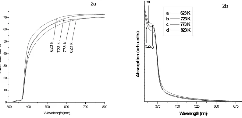
3.2. Figure 2a. Shows the UV transmittance
of the films at four annealed temperatures. The graph shows that there is slight decrease in transmittance in the visible region as the sintering temperature increases. Fig. 2b indicates a sharp absorption edge around 370 nm which corresponds to the band gap of 3.35 eV of ZnO. Since the transmittance of the film annealed at 773k shows less transmittance compared to other films this film could absorb electromagnetic radiation more and hence could be a promising candidate as n-type semiconductor for device fabrication of solar cells.
3.3. Figure 3(a) and 3(b) shows the
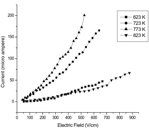
conductivity measurement apparatus11. Dark and photo conductivities studies were carried out using two probe technique in which thin copper wires (0.14mm diameter) were used as electrodes. Given the resistance of the material, four-probe method was thought not necessary. The wires were fixed on the films using silver paint. The distance between the electrodes was maintained at 1mm for all the samples. The ends of the wires were connected in series with a DC power supply (0-500V) and a picoammeter (keithley 6485). The applied field between the electrodes was increased from 0 to 900 V/cm and the current was measured in micro-ampere. A UV light was used to measure the photocurrent for various applied fields. To study the variation of current with temperature the sample was kept inside a pyrex cylinder of diameter 5cm (length
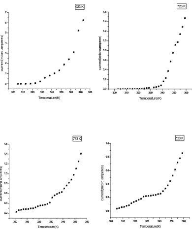
75cm) with kanthal wire wound around it. The ends of the wire were connected to a variac for heating. A probe connected to a temperature monitor was used to measure the temperature of the sample. The electrodes of the sample were connected to the DC power supply and the picoammeter in series. The dark and the photo currents were measured by varying the supply voltage. The photo current is found to increase with increase in annealing temperature and becomes maximum for 773k, beyond this i.e. for 823k the conductivity decreases .The increase in the photo current compared to dark current for constant field is shown in table 1 and table 2 it is also observed that the dark and photo current increase with increase in field. The dark current is measured for various temperatures ranging from 300K to 400K for constant applied field. The temperature dependent graph is drawn between Ln(I) vs 1/kT[12,13].The activation energy is calculated from the equation I=IO exp[-Ea/kT],where Ea is the activation energy (in eV). The temperature dependant conductivity shows that the activation energy changes with change in annealing temperature as shown in Table.3 and it is minimum for up to 773K.This is the reason for increased photo conductivity for films annealed at 773K. The activation energy indicate the presence of donor levels very close to the conduction band.
3.4. Fig 7 shows the exponential time
dependence of the current in two different regions following
I=IO(1-e -t/τ1
) and I=IO(e -t/τ2
Fig. 1. SEM images of the ZnO thin film on a glass substrate preheated at 623k for 15 minutes and annealed at 623K (a) , 723K(b) , 773K(c) and 823K(d) for 60 minutes.
Fig 2a & 2b Transmission and absorption spectra of the ZnO films annealed at 623K, 723K, 773K & 823K.
300 400 500 600 700 800
0 10 20 30 40 50 60 70
2a
8
2
3
k
7
7
3
k
7
2
3
k
6
2
3
k
T
ra
n
s
m
it
ta
n
c
e
%
Wavelength(nm)
375 450 525 600 675
2b
d
c
b
a
A
b
s
o
rp
ti
o
n
(
a
rb
.u
n
it
s
)
Wavelength (nm) a 623 K
b 723 K
c 773 K
Fig. 3 (a) & Fig. 3 (b) Schematic representation of the conductivity and temperature dependant conductivity apparatus.
Fig. 4. Photo conductivity for films annealed at different temperatures.
D.C
pA
D.C
pA
0 100 200 300 400 500 600 700 800 900
0 50 100 150 200
C
u
rr
e
n
t
(m
ic
ro
a
m
p
e
re
)
Electric Field (V/cm)
Fig. 5. Temperarature dependent conductivity for films annealed at different temperatures. 300 310 320 330 340 350 360 370 380
0 1 2 3 4 5 6 7 c u rr e n t( m ic ro a m p e re s ) Temperature(K) 623 K
300 310 320 330 340 350 360 0.0 0.2 0.4 0.6 0.8 1.0 1.2 1.4 1.6 c u rr e n t( m ic ro a m p e re ) Temperature(K) 723 K
300 310 320 330 340 350 360 0.0 0.2 0.4 0.6 0.8 1.0 c u rr e n t( m ic ro a m p e re s ) Temperature(K) 823 K
Fig.6. Ln(I) vs 1/kT for films annealed at different temperatures.
1.9 2.0 2.1 2.2 2.3 2.4
-19 -18 -17 -16 -15 -14 -13 -12 -11
L
n
(
I)
1/kTx1020 J-1
623 K
2.0 2.1 2.2 2.3 2.4
-22 -21 -20 -19 -18 -17 -16 -15 -14 -13
L
n
(I
)
1/kTx1020 J-1
723 K
2.0 2.1 2.2 2.3 2.4
-15.5 -15.0 -14.5 -14.0 -13.5
Ln
(I)
1/kTx1020
J-1
773 K
2.0 2.1 2.2 2.3 2.4
-17.5 -17.0 -16.5 -16.0 -15.5 -15.0 -14.5 -14.0 -13.5
L
n
(I
)
1/kTx1020 J-1
is found that the film annealed at 773K show a very less rise time and significantly larger decay time. This shows the film annealed at 773K is more photo sensitive than other films.
3.5. The infrared spectra are recorded for the
thin films of ZnO prepared by annealing at 623K, 723K, 773K and 823K. Films annealed at 623K and 823K show same kind of spectral pattern and the films annealed at 723K and773K also show similar spectral pattern but different from the former. The absorptions at 3526 and 2922 cm-1 may be due O-H stretching of moisture and C-H stretching of aliphatic organic residues, respectively. The Zn-O stretching frequency
is observed as separate absorption band at around 810 cm-1 for the samples annealed at 623K and 823K, whereas it is not observed for the samples annealed at 723K and 773K. This suggests that the ZnO bonding pattern in samples annealed at623K and823k could be different from samples annealed at 723K and 773K. The Zn and O atoms may be weakly bonded in samples annealed at 623K and 823K to appear at lower energy and strongly bonded in the samples723K and773K to appear at higher energy. As a result the current output of the samples annealed at 723K and 773K is high and that of samples annealed at 623K and 823K is low.
Fig.7. Photo response curve for ZnO films annealed at different temperature.
0 100 200 300 400 500 600 700 800
0.0 0.2 0.4 0.6 0.8 1.0 1.2 1.4 1.6 1.8 2.0 2.2 2.4 2.6 2.8 3.0
p
h
o
to
c
u
rr
e
n
t(
m
ic
ro
a
m
p
e
re
)
time(s)
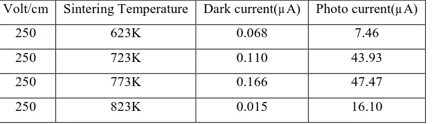
Table 1. Variation in dark and photo currents for a fixed field of 250V/cm
Volt/cm Sintering Temperature Dark current(µ A) Photo current(µA)
250 623K 0.068 7.46
250 723K 0.110 43.93
250 773K 0.166 47.47
250 823K 0.015 16.10
Table 2. Variation in dark and photo current for a fixed field of 500V/cm
Volt/cm Sintering Temperature Dark current(µ A) Photo current(µA)
500 623K 0.148 34.41
500 723K 0.307 114.51
500 773K 0.482 124.58
500 823K 0.037 37.92
Table 3.Variation of Activation Energy with sintering temperature
Annealing Temperature (K) Activation Energy(eV)
623K 0.711
723K 0.641
773k 0.554
823k 0.804
Table 4. Response time of ZnO films annealed at different temperature
Annealing temperature(K) Rise time (sec) Decay time (sec)
623 311 20
723 72 135
773 34 110
4. CONCLUSION
ZnO thin films annealed at 623K, 723K, 773K & 823K prepared by spin coating technique have been studied for their surface, optical and electrical properties.
1. Optical transmission spectra reveal that the ZnO thin films transmission decreases with increase in annealing temperature. The absorption spectra show maximum absorption for 773K annealed film in the UV region.
2. The conductivity studies shows the increase in the dark and photo conductivity as the annealing temperature increases and is maximum for the film annealed at 773K The temperature dependent conductivity shows that activation energy is lowest for the film annealed at 773K.
3. Among the four films annealed, the film annealed at 773K has strongly bonded Zn and O atoms.
It has been observed that spin-coating as well as annealing enhance the electric conductivity in ZnO. While spin-coating ensures smooth and uniform thickness of the film, annealing reduces the grain-boundary bolstering the bonds between Zn and O atoms. However, beyond the optimum temperature the film begins to decompose and also formation of cracks would crop in, thereby reducing the conductivity. It has been shown that the
studies of absorption/transmittance, conductivity, activation energy, and bonding are temperature dependence upto an optimum temperature.
REFERENCES
1. J. A Sans, A. Segure, et al., Thin solid
films 453-454, 251 (2004).
2. K. Ogata, K. Koike, T. Tanite, et al., J.
Cryst. Growth 251, 623 (2003).
3. H. Chaowang, Zhenguo Ji, Kun liu, Yin Xiang and Zhizhen Ye, J. Cryst. Growth 259, 279 (2003).
4. S. Liang, H. Sheng, Y. Liu, Z. Huo, Y. Lu and H. Shen, J. Cryst. Growth 225, 110 (2001).
5. Kwang – Sik kim, Hyoun et al., Mat.
Sci. Eng B 98, 135 (2003).
6. P. P. Sahay, S. Tewari and R. K. Nath.
Cryst. Res. Technol. 723-729 422 (2007)
7. Zhenguo Ji, Chengxin Yang, Kun Liy, and Zhizhen Ye, J. Cryst. Growth 253, 239 (2003).
8. Ji Zhenguo, Yang Chengxin, et al., J.
Cryst. Growth 253, 243 (2003).
9. Y. R. Ryu, T. S. Lee, and H.W White, J.
Cryst. Growth 261, 502 (2004).
10. G. Srinivasan and J. Kumar. Cryst. Res.
Technol. 41, 893-896 (2006).
11. D. Ponniah, F. Xavier Physica B:
Condensed Matter, Volume 392, Issues
1-2, 15 April, Pages 20-28 (2007). 12. Francis P. Xavier, Anto Regis Inigo and
George J. Goldsmith. J. Porphyrins
13. S. Lawrence Selvaraj, Francis P. Xavier.
Journal of crystal Growth 233, 583-590
(2001).
14. S. Mridha, D. Basak Materials Research
Bulletin 42, 875–882 (2007).
15. Francis P. Xavier and George J.