The Effect of Fluorine Doping on the Characteristic
Behaviour of CdTe
OJO, A. A. and DHARMADASA, I <http://orcid.org/0000-0001-7988-669X>
Available from Sheffield Hallam University Research Archive (SHURA) at:
http://shura.shu.ac.uk/13111/
This document is the author deposited version. You are advised to consult the
publisher's version if you wish to cite from it.
Published version
OJO, A. A. and DHARMADASA, I (2016). The Effect of Fluorine Doping on the
Characteristic Behaviour of CdTe. Journal of Electronic Materials, 45 (11),
5728-5738.
Copyright and re-use policy
See
http://shura.shu.ac.uk/information.html
Sheffield Hallam University Research Archive
1
The Effect of Fluorine Doping on the Characteristic Behaviour of CdTe
A. A. Ojo* and I. M. Dharmadasa
Materials and Engineering Research Institute, Sheffield Hallam University, Sheffield, S1 1WB, UK. *Email: [email protected]; Tel: +44 743 898 4557 Fax: +441142256930
ABSTRACT
Fluorine which is an n-type dopant of Cadmium Telluride (CdTe) thin films was included during growth from a cadmium nitrate (Cd(NO3)2·4H2O) bath using electrodeposition technique. The fluorine concentration in the Cd(NO3)2·4H2O baths were varied between 0.5 ppm to 50 ppm in order to determine its effect on the optical, structural, morphological and electrical properties of the as-deposited and the post-growth treated layers. These characterisations were carried out using X-ray diffraction (XRD), Ultraviolet–visible (UV-Vis)
spectrophotometry, scanning electron microscopy (SEM), energy dispersive x-rays spectroscopy (EDX), Photoelectrochemical (PEC) cell measurement, direct current (DC) conductivity measurement and fully fabricated device characterisation. The results are systematically reported in this paper.
2
1. INTRODUCTION
Binary semiconductor compound such as CdTe has been extensively explored and tailored towards photovoltaic applications. Especially for CdS/CdTe thin film configuration which has achieved efficiency up to 21.5% in 2015 [1], [2]. The efficiency of the fabricated cells depends on all the layers and the corresponding interface states with special emphasis on the post-growth treatment with halogens such as chlorine and fluorine. CdCl2 post-growth treatment has been reported in the literature as an important and sensitive step due to the enhancement in the photoelectrical, structural and morphological properties of CdTe layers which are important to achieve high efficiency solar cell [3]–[5]. With emphasis on fluorine, Rios-Flores [6] and Echendu et al [7] amongst other authors have also reported further enhancement in CdTe properties with the inclusion of fluorine during CdTe growth and/or in CdCl2 post-growth treatment respectively. The inclusion of fluorine is deemed to increase the conductivity CdTe layer due to the excess electrons supplied by fluorine. Literature on the optimal concentration of fluorine in CdTe has not been well established in electrodeposited CdTe bath. Therefore, this work focuses on the optimisation of extrinsic fluorine doping concentration in CdTe thin films electrodeposition bath to achieve better material and device properties.
2. EXPERIMENTAL DETAILS
2.1 Electrolyte and Substrate Preparations
3
computerized GillAC potentiostat connected to a two-electrode electroplating system. The two electrode configuration was utilised for its simplicity and to isolate the effect of fluorine doping. Prior to the deposition of CdTe layer, the cyclic voltammograms of the resulting electrolytes were reported to determine the possible growth voltage range of CdTe. The FTO substrate was cleaned with the use of ultrasonic bath containing soap solution for 15 min and rinsing with deionised water. Afterwards, it was then cleaned with methanol and acetone to remove any grease and rinsed thoroughly in deionised water. The optimal cathodic voltage of the CdTe layer was determined to be ~1370 mV based on optical, structural, morphological and compositional analysis [8] on electrolytic bath containing Cd(NO3)2·4H2O and TeO2 as the cadmium and tellurium precursors.
2.2 Experimental Techniques
The information about the level of crystallinity and phases identification of deposited layers were obtained using Philips PW 3,710 X’pert diffractometer with Cu-Kα monochromator of wavelength λ=1.54 Å. While the X-ray generator tension and current were adjusted to 40 kV and 40 mA respectively for these experiments. The optical properties of the grown CdTe thin films were studied using Cary 50 Scan UV-Vis spectrophotometer within the wavelength range of 200-1000 nm at room temperature. The morphological and compositional analysis of the CdTe layers was studied using FEI Nova 200 NanoSEM equipment at a magnification of ×60,000. The electrical conductivity type of the layers was determined using Photoelectrochemical Cell (PEC) measurements. The DC conductivity of grown CdTe layers and the fully fabricated solar cell parameters were measured using Rera Solution I-V measurement system.
3. RESULTS AND DISCUSSION
3.1 Structural Analysis
4
although further experimentation is still required. Increasing the F-doping concentration above this point results
in a reduction in CdTe (111)C reflection intensity, incomplete crystallisation, and low adhesion to the underlying FTO substrate [9], [10] as shown in Figure 2. This observation can be explained by the initial replacement of tellurium ions with fluorine ions in the CdTe lattice up to 20 ppm which aids the crystallisation of CdTe as shown in Figure 1. However, a further increase in F-doping concentration may easily be incorporated within the crystal lattice but not occupying the proper lattice position whereby increasing disorderliness within the crystal structure [11], [12].
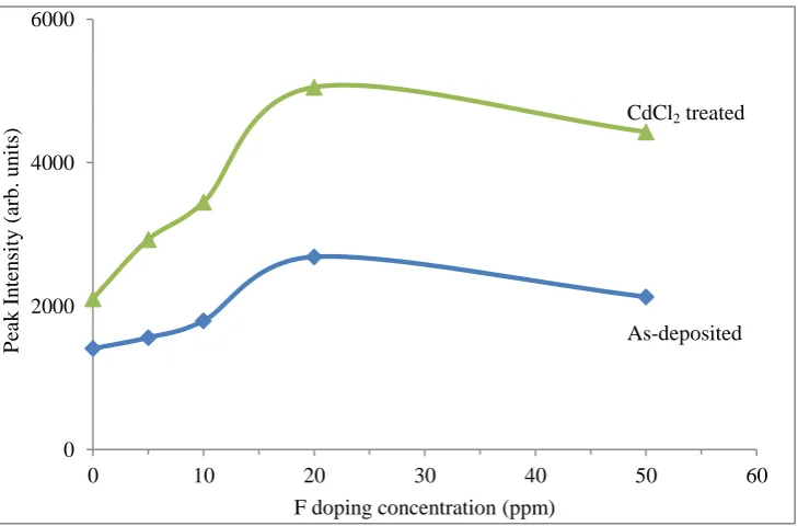
The XRD reflection intensity of layers improved after CdCl2 post growth treatment at 400˚C for 20 min in air as shown in Figure 1(b) and Figure 2. This might be attributed to grain growth and re-crystallisation of the crystal
structure. The highest intensity was observed at 20 ppm fluorine concentration. For clarity, the observed CdTe (111)C reflection intensity was plotted against the concentration of F-doping in CdTe bath as shown in Figure 2. The initial reductions in full width at half maximum (FWHM) and resulting increase in crystallite size were observed with increasing F-doping concentration to 20 ppm in the as-deposited CdTe layers as shown in Table I, while a further increase in F-doping concentration resulted in a reduction in the crystallite size. This observation can be attributed to the replacement of Te atoms from Group VI (atomic radius of 1.4 Å) with F atoms having a comparatively low atomic radius of ~0.5 Å from Group VII. This might lead to the contraction of the CdTe lattice, hence, a reduction in crystallite size [13], [14] with increasing F atom concentration as observed in the as-deposited CdTe layer grown above 20 ppm concentration as shown in Table I. The calculated crystallite size, D, for all the CdCl2 treated CdTe layers using Scherrer's equation were all ~ 52.4 nm. The observation of the same value (~52.4 nm) for all F-doping concentration indicates the limitation of the use of Scherrer equation for materials with larger grains [15].
The extracted XRD data from these CdTe work matches the Joint Committee on Powder Diffraction Standards
(JCPDS) reference file number 01-075-2086-cubic. The crystallite size, D was calculated using the Scherrer's formula:
cos 94 . 0
D (1)
5
0 2000 4000 6000
0 10 20 30 40 50 60
P ea k I n ten sity ( ar b . u n its )
F doping concentration (ppm)
[image:6.595.96.543.90.320.2]As-deposited CdCl2 treated
[image:6.595.87.452.374.614.2]Figure 2: Comparative analysis of CdTe (111)C reflection intensity for as-deposited and CdCl2 treated layers grown at different fluorine doping concentrations
Figure 1: Typical XRD patterns of CdTe at different fluorine doping concentrations for (a) As-deposited CdTe layers and (b) CdCl2 treated CdTe layers at 400˚C for 20 min in air.
0 5000 10000 15000 20000
10 30 50 70
P ea k I n ten sity ( ar b . u n its ) 2θ (degrees) 0 ppm 5 ppm 10 ppm 20 ppm 50 ppm
(b)
(1 1 1 )CCdCl2 treated
* * #
* FTO # CdxTeOy
*
0 5000 10000
10 30 50 70
P ea k I n ten sity ( ar b . u n its ) 2θ (degrees) 0 ppm 5 ppm 10 ppm 20 ppm 50 ppm
(a)
(1 1 1 )C As-deposited * * # * FTO # CdxTeOy6
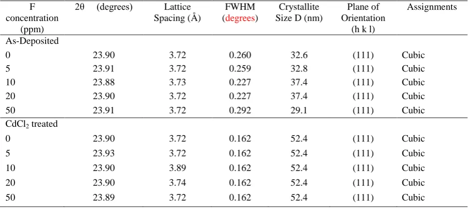
Table 1: The XRD analysis of CdTe layers grown at different fluorine concentrations.
F concentration
(ppm)
2θ (degrees) Lattice Spacing (Å)
FWHM (degrees)
Crystallite Size D (nm)
Plane of
Orientation (h k l)
Assignments
As-Deposited
0 23.90 3.72 0.260 32.6 (111) Cubic
5 23.91 3.72 0.259 32.8 (111) Cubic
10 23.88 3.73 0.227 37.4 (111) Cubic
20 23.90 3.72 0.227 37.4 (111) Cubic
50 23.91 3.72 0.292 29.1 (111) Cubic
CdCl2 treated
0 23.90 3.72 0.162 52.4 (111) Cubic
5 23.93 3.72 0.162 52.4 (111) Cubic
10 23.90 3.89 0.162 52.4 (111) Cubic
20 23.90 3.74 0.162 52.4 (111) Cubic
7
3.2 Analysis of optical absorption
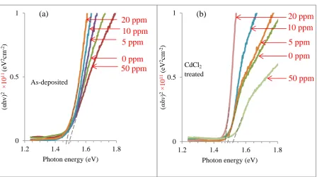
The optical bandgap of the as-deposited and CdCl2 treated CdTe layers was analysed by plotting the (αhv)2 against photon energy (hν) as shown in Figure 3 where α is the absorption coefficient of the CdTe, h is Planck's constant and v is the frequency of the electromagnetic radiation. Noticeably in Figure 3(a), stronger absorption edges were observed with increasing F-doping concentration in the as-deposited CdTe layers with no observable influence on the bandgap energy. The observed bandgap energy for the test samples falls within the range of 1.47 eV to 1.50 eV. A dissimilar trend was observed after CdCl2 treatment of the CdTe layers as shown in Figure 3(b). For CdTe doped with (0 to 20) ppm fluorine, a rise in the absorption edge, coupled with a reduction in the bandgap energy was observed. These observations can be attributed to improvement in material properties such as grain size, crystallinity amongst others. An increase in the doping above 20 ppm resulted in a reduction in the gradient of the optical absorption edge and also an increase in the optical bandgap [4], [16]. This might be due to material quality deterioration such as sublimation of CdTe layer. It could be deduced from the optical parameters that fluorine doping concentration of ~20 ppm gives best optical property with 1.46 eV bandgap. This observation is in accord with the structural and morphological observations.
Figure 3: Optical absorption edge of CdTe with different doping concentrations of fluorine for (a) as-deposited, and (b) CdCl2 treated (at 400˚C for 20 min in air) layers.
0 0.5 1
1.2 1.4 1.6 1.8
(α
hv)
2 ×
10
11
(eV
2cm -2)
Photon energy (eV) As-deposited
(a)
20 ppm
10 ppm
5 ppm
0 ppm
50 ppm
0 0.5 11.2 1.4 1.6 1.8
( αhv ) 2× 10 11 (eV 2cm -2)
Photon energy (eV) CdCl2
treated
(b)
20 ppm
10 ppm
5 ppm
0 ppm
[image:8.595.75.524.394.645.2]8
3.3 Morphological Analysis
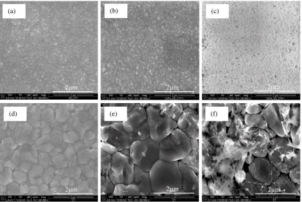
[image:9.595.75.510.314.604.2]Figure 4(a – c) represents the as-deposited CdTe layers containing 0, 20 and 50 ppm F-doping concentration respectively, while Figure 4(d – f) are the resulting micrographs after CdCl2 treatment respectively. The as-deposited layers show full coverage of the underlying FTO substrate with an observable reduction in grain size and indistinct crystal boundary at 50 ppm F-doping concentration. The morphology reveals that the formation of grain boundaries has been suppressed due to the presence of superfluous fluorine at high concentration. The CdCl2 treated layers show grain growth to ~(1, 1.9 and 1.4) µm for (0, 20 and 50) ppm F-doping concentration respectively. It could be said that the addition of fluorine to ~20 ppm is advantageous to grain growth while the inclusion of fluorine to 50 ppm is detrimental as observed in Figure 4(f). Although large grains were observed, the formation of pin-holes and loss of CdTe layer will be detrimental to device parameters due to shunting.
Figure 4: SEM micrographs for CdTe layers grown with F-doping concentration of (a) 0 (b) 20 and (c) 50 ppm with CdCl2 treated layers with F-doping of (d) 0 (e) 20 and (f) 50 ppm.
(f)
2μm (e)
2μm
(c)
2μm
(d)
2μm (a)
2μm
(b)
9
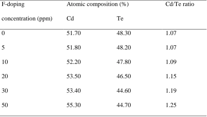
3.4 Compositional Analysis
The presence of base elements (Cd and Te) was observed at all doping concentrations of fluorine and their percentage concentration for the as-deposited CdTe thin films is presented in Table II. It was observed that the atomic composition of Cd was greater than Te in all the explored fluorine doping concentration range with an increase in the Cd/Te atomic composition ratio as shown in Table II. This observation may not be due to the continuous replacement of Te ions with F ions at ppm level in the crystal lattice. It is important to note that due to the presence of nominal fluorine in ppm level in the electrolytic bath, the atomic concentration of fluorine in CdTe thin films at different concentration cannot be determined. However, the presence F in the electrolyte seems to act as a catalyst to produce Cd-rich layers. As argued by Dharmadasa et al., the defect levels in Cd-rich material is lower than those in Te-rich material [17]. Therefore, the CdTe layers doped with F should produce solar cell devices with enhanced parameters.
In addition to the presence of Cd and Te atoms, the EDX results may show the presence of Sn, Si, F and O which is due to the underlying glass/FTO substrate and the oxidation of CdTe film surface. The observation made from the compositional analysis gives a clue why the conductivity type discussed in Section 3.7.1 is always n-type.
Table II: Summary of the compositional analysis of as-deposited CdTe layers at different F doping
concentration in CdTe bath.
F-doping
concentration (ppm)
Atomic composition (%) Cd/Te ratio
Cd Te
0 51.70 48.30 1.07
5 51.80 48.20 1.07
10 52.20 47.80 1.09
20 53.50 46.50 1.15
30 53.40 44.60 1.19
[image:10.595.134.465.486.673.2]10
3.5 Analysis of electrical properties
3.5.1 Photoelectrochemical (PEC) Cell Study
Figure 5 shows a typical photoelectrochemical cell measurement of CdTe doped with different concentration of fluorine. It was observed that both the as-deposited and CdCl2 treated CdTe layers were all n-type in electrical conduction. This might be due to the presence of fluorine, an n-type dopant in the electrolytic bath. It has been well documented in the literature that the inclusion of halogen in CdTe serves as electron donor impurity by replacing Te atoms in the CdTe lattice with halogen atoms with higher valence electrons. This introduces additional free electron and therefore makes the CdTe n-type. It should be noted that n- , i- , and p- CdTe layers can be grown from the 0 ppm F-doping (i.e. un-doped) CdTe bath through growth voltage alteration [18]. As shown in Section 3.4, the presence of F in the bath replaces and reduces the excess deposition of Te. The Cd-richness makes the material more n-type in electrical conduction. The increase in observed PEC signal with increasing F-doping concentration might be due to increasing free electron from the F-doping and increased Cd-richness.
As observed in Figure 5, the PEC signals for all CdCl2 treated CdTe layers in this work tend to reduce. This difference can be attributed to the improvement in the material electronic properties by the sublimation of excess element during the annealing process or the formation of CdTe through chemical reaction between precipitated Te in the layer and excess Cd from CdCl2. Furthermore, the observed changes can also be attributed to the doping effect of fluorine.
-200 -150 -100 -50 0
0 10 20 30 40 50
P
E
C
s
ig
n
al
(m
V)
F-doping concentration (ppm)
[image:11.595.75.440.538.750.2]As-deposited CdCl2 treated
11
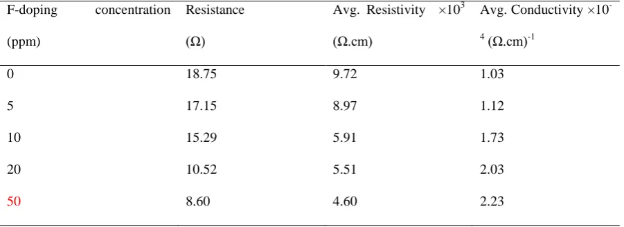
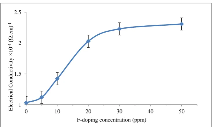
3.5.2. DC Conductivity Study
The DC conductivity measurement was carried out on glass/FTO/n-CdTe/Al structure with different F-doping concentrations. The CdTe layers utilized in this experiment were ~1.1 µm thick and CdCl2 treated at 400˚C for 20 min in air. The evaporated Al on the CdTe was to make an ohmic contact, while the I-V measurements were taken in dark condition. By measuring several ohmic contacts, the average resistance of the glass/FTO/
n-CdTe/Al structures were determined. The electrical resistivity and conductivity were calculated with known contact area and film thickness.
[image:12.595.74.525.509.673.2]A typical DC conductivity against F-doping concentration in CdTe bath is plotted in Figure 6. It was observed that the introduction of fluorine increases the electrical conductivity of the layers which saturate at ~20 ppm fluorine concentration. The saturation of DC conductivity further suggests the solubility limit of fluorine in CdTe lattice as discussed in Section 3.1 [11]. Therefore, an increase in F-doping above 20 ppm results into superfluous addition under this experimental condition. As explained in Section 3.5.1, the inclusion of fluorine into the crystal lattice introduces free electrons which result into increased conductivity. The enrichment of Cd also contributes to the electrical conductivity and the resultant effect is measured using this method.
Table III: Electrical resistivity and conductivity as a function of fluorine doping concentration in the electrolytic
bath.
F-doping concentration (ppm)
Resistance (Ω)
Avg. Resistivity ×103 (Ω.cm)
Avg. Conductivity ×10 -4 (Ω.cm)-1
0 18.75 9.72 1.03
5 17.15 8.97 1.12
10 15.29 5.91 1.73
20 10.52 5.51 2.03
12
3.6 Solar cell device characterisation
After the structural, optical, morphological, compositional and electrical study on the CdTe layers whose baths were doped with different concentration of fluorine was completed; similar CdTe of ~1.1 µm thick from (0, 20 and 50) ppm F-doped bath was grown on a pre-treated glass/FTO/CdS substrate and capped with electrodeposited p-type CdTe from the 0 ppm F-doped bath.
The 150 nm thick CdS layer utilised in the glass/FTO/n-CdS/n-CdTe/p-CdTe configuration was electrodeposited from an electrolytic bath containing 0.03 M ammonium thiosulphate ((NH4)2S2O3) and 0.3 M cadmium chloride hydrate (CdCl2·xH2O) at an optimised cathodic voltage of 1200 mV based on morphological, compositional, structural, electronic and optical analysis [19]. The glass/FTO/CdS layer was CdCl2 treated at 400°C in air prior to the deposition of other layers. The incorporation of the p-CdTe layer is to pin the fermi level very close to the valence band. The schematic diagram and the band diagram of the fabricated solar cells are shown in Figure 7. It is important to note that during the CdCl2 treatment of n-CdS/ n-CdTe/p-CdTe structure, there is an inter-diffusion of Te and S which results in the formation of CdSxTe1−x intermediate material at the CdS/CdTe interface [20], [21]. This intermediate material is expected to have a bandgap between those of CdS and CdTe, thus causing a grading in bandgap between CdS and CdTe.
1 1.5 2 2.5
0 10 20 30 40 50
E
lectr
ical
C
o
n
d
u
ctiv
ity
×
10
-4 (Ω.
cm
)
-1
[image:13.595.75.446.114.334.2]F-doping concentration (ppm)
13
(a)
glass FTO Au
P-CdTe
n-CdTe
n-CdS
Sunlight
(b)
n
-C
d
S
n-CdTe
ϕ
bFTO front contact
Metal back contact e
e
e
h
h
h a
a = CdSxTe1-x
p-CdTe
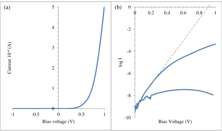
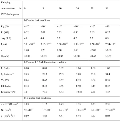
The layer (glass/FTO/n-CdS/n-CdTe/p-CdTe) was heat treated with CdCl2 at 400˚C for 20 min in air. The surface was etched using a solution containing K2Cr2O7 and concentrated H2SO4 for acid etching and solution containing NaOH and Na2S2O3 for basic etching. 2 mm diameter Au was evaporated at a vacuum pressure of ~10-4 Nm-2. The glass/FTO/n-CdS/n-CdTe/p-CdTe/Au device was analysed using both I-V and C-V characteristic measurements to determine their device parameters. Typical linear-linear and log-linear I-V curves measured in dark condition for device incorporating CdTe from the 20 ppm F-doped CdTe bath is shown in Figure 8, linear I-V curve under 1.5 AM illuminated condition is shown in Figure 9, typical Schottky–Mott plot of glass/FTO/n-CdS/n-CdTe/p-CdTe/Au layer is shown in Figure 10, while the device parameters are presented in Table IV for comparison. The effective Richardson constant (A*) has been calculated to be 13.22 Acm-2K-2 for CdTe.
14
As observed in the dark I-V Section of Table IV, the shunt resistance (Rsh) were comparatively high across all
F-doped CdTe devices but low for the 50 ppm F-F-doped materials. Low Rsh values of a solar device as explained by Soga, 2004 can be directly related to low semiconductor material quality which might be due to the inclusion of voids, gaps, high dislocation density within the semiconductor material [22]. It should be noted that Rsh is more
dominant in low light condition and may result in the reduction in Fill Factor (FF) and the open circuit voltage (Voc) [23]. It is interesting to know that this observation correlates with the optical and morphological
summaries on the CdTe material property presented in Sections 3.2 and 3.3 respectively.
The CdTe layers grown with (0, 5, 10 and 20) ppm F-doped baths show good rectification factor (RF) with values higher than 3 orders of magnitude, while a drastic reduction in the RFto ~ 100.9 is recorded for device samples with higher F-doping concentration above 20 ppm. As reported by Dharmadasa 2013, the minimum of ~103 RF value is sufficient for an efficient solar cell [24], however, higher RF values show high quality rectifying property of the devices and desirable for solar cells with very high efficiencies. The drastic reduction in the RF value can be attributed to the deterioration of the CdTe material at higher F-doping concentrations.
-10 -8 -6 -4 -2 0
0 0.2 0.4 0.6 0.8 1
lo
g
I
Bias Voltage (V)
(b)
0 1 2 3 4 5
-1 -0.5 0 0.5 1
C
u
rr
en
t
1
0
-4 (
A
)
Bias voltage (V)
(a)
[image:15.595.73.527.104.371.2]15
Furthermore, the device samples grown from baths containing 0 ppm to 20 ppm F-doping concentration shows an ideality factor (n) between 1.00 and 2.00, while higher n values are observed at higher F-doping concentration. This indicates that the current transport mechanism of devices grown from electrodeposition baths containing between 0 ppm to 20 ppm F-doping concentration is dominated by both thermionic emission and recombination & generation (R&G) processes in parallel [25]. Ideality factor value, >2, observed for devices grown from CdTe bath with F-doping concentration above 20 ppm shows that the current transportation mechanism is not limited to thermionic emission and (R&G) but also due to the tunnelling of high energy electron through the barrier height [26], which in turn causes a reduction in the barrier height ɸbas observed in
16
Table IV: Device parameters from I-V (dark condition), I-V (illuminated at 1.5 AM) and C-V (dark condition)
measurements.
F-doping
concentration in CdTe bath (ppm)
0 5 10 20 30 50
I-V under dark condition
Rsh (Ω) ~106 ~106 ~106 ~106 ~105 ~103
Rs (kΩ) 0.52 2.07 5.33 0.50 2.63 0.22
log (R.F) 4.8 4.4 3.2 4.2 2.2 0.9
Io (A) 5.01×10⁻¹⁰ 3.16×10⁻¹⁰ 3.98×10⁻¹⁰ 1.58×10⁻⁹ 1.58×10⁻⁷ 7.94×10⁻⁶
n 1.60 1.70 1.70 1.60 >2.00 >2.00
Φb (eV) >0.82 >0.83 >0.83 >0.80 >0.67 >0.57 I-V under 1.5 AM illumination condition
Isc (mA) 0.80 0.89 0.92 1.06 1.06 1.06 Jsc (mAcm-2) 25.5 28.3 29.3 33.8 33.8 34.4
Voc (V) 0.64 0.62 0.67 0.73 0.62 0.35
Fill factor 0.43 0.43 0.45 0.50 0.44 0.37 Efficiency (%) 7.01 7.56 8.83 12.32 9.21 4.37
C-V under dark condition
σ ×10-4 (Ω.cm)-1 1.03 1.12 1.73 1.75 2.23 2.31 ND (cm-3) 9.4×10¹⁴ 1.7×10¹⁴ 1.9 ×10¹⁴ 1.8 ×10¹⁴ 5.2 ×10¹⁵ 7.7 ×10¹⁶ µ (cm2V-1s-1) 0.69 4.23 5.61 5.94 0.27 0.02
17
Figure 10 shows a typical Schottky-Mott plot of glass/FTO/n-CdS/n-CdTe/p-CdTe/Au layer using the 20 ppm F-doped CdTe bath for the growth of n-CdTe layer. The C-V measurements were performed in dark condition at a bias range of (-1.00 to 1.00) V with 1 MHz AC signal at 300 K. The built-in potential (Vbi) and doping density
(ND) in this configuration can be determined using the Mott-Schottky plot as shown in Figure 10 and equations
(2) to (4)
)
(
2
1
2
2 R bi
D s
V
V
N
eA
C
(2)
slope
eA
N
r D
2 02
(3) 22
A
eN
Slope
D s
(4)where C is the capacitance, ɛs is the semiconductor permittivity, ɛr is the relative dielectric constant, ɛo is the permittivity of free space, e is the electronic charge, A is the area of the contact, ND is the donor concentration,
VR is the reverse bias voltage and Vbiis the built-in potential. The slope and the intercept of the C-2 versus V plot
is given by equation (4). The ɛr is taken as 11 and the effective density of states in the conduction band (Nc) was
calculated to be 9.16×1017 cm-3 using equation (5), where, k is the Boltzmann’s constant, me* is the effective
[image:18.595.93.461.454.616.2]electron mass, T is the temperature, and h is the plank’s constant.
Figure 9: Linear I-V curve of glass/FTO/n-CdS/n-CdTe/p-CdTe/Au under AM 1.5 for 0, 20 and 50 ppm doped CdTe baths.
-40 -30 -20 -10 0 10
-100 100 300 500 700
18
2 3 2 * 2 2 h kT m N e C (5)The carrier mobility µ⊥ was calculated using equation (6) with the assumption that all donor atoms (ND) are
ionised at room temperature, therefore, nND as shown in equation (6). All the calculated parameters are shown in Table IV.
e
N
ne
D
(6)As observed in Table IV, the ND for devices grown using the 0 to 20 ppm F-doping concentration was ~1014 cm
-3. An increase in the N
D to ~1017 cm-3 was observed above 20 ppm F-doping concentration. Investigation on the
optimum ND of CdTe has been reported in the literature to be ~1014 [15, 16, 17]. An increase in the mobility
was observed within the range of 5 to 20 ppm F-doping concentration. Above this F-doping concentration range, a reduction in the mobility was observed. The reduction in mobility might be due to the presence of high concentration of defects (R&G centres) as depicted by the high ideality factor on the devices.
0 10 20 30 40 50
0 0.2 0.4 0.6 0.8 1
C
-2 ×
10
18 (F -2)
Bias voltage (V) 0 2 4 6
-0.5 0 0.5 1
C ap ac itan ce × 10 -10 ( F)
[image:19.595.75.445.196.485.2]Bias voltage (V)
19
4. CONCLUSIONS
In this work, we have explored the effect of fluorine doping (in CdTe electrolytic bath) on CdTe layer as it affects it’s structural, optical, morphological and compositional. properties. Further investigation on the electronic property of the CdTe layer was also carried out by incorporating the layer in a glass/FTO/n-CdS/
n-CdTe/p-CdTe/Au device configuration. An optimal F-doping concentration of ~20 ppm was observed under all material and device characterisation with a DC conductivity of 1.75×10⁻⁴ (Ω.cm)-1, short circuit current density
Jsc of 33.76 (mAcm-2), doping density ND of 1.8×10¹⁴, mobility μ of 5.94 (cm2V-1s-1) and conversion efficiency
of 12.3%. These observed parameters can still be improved through more precise processing steps, improved material quality, and improved metal/semiconductor contact property amongst others. Development of
multilayer graded bandgap devices is in progress towards achieving the highest possible efficiency.
Acknowledgement
20
REFERENCES
[1] M. A. Green, K. Emery, Y. Hishikawa, W. Warta, and E. D. Dunlop, “Solar cell efficiency tables (version 46),” Prog. Photovoltaics Res. Appl., vol. 23, no. 7, pp. 805–812, 2015.
[2] “First Solar raises bar for CdTe with 21.5% efficiency record: pv-magazine.” [Online]. Available: http://www.pv-magazine.com/news/details/beitrag/first-solar-raises-bar-for-cdte-with-215-efficiency-record_100018069/#axzz3rzMESjUl. [Accessed: 20-Nov-2015].
[3] B. M. Başol, “Processing high efficiency CdTe solar cells,” Int. J. Sol. Energy, vol. 12, no. 1–4, pp. 25– 35, 1992.
[4] A. Bosio, N. Romeo, S. Mazzamuto, and V. Canevari, “Polycrystalline CdTe thin films for photovoltaic applications,” Prog. Cryst. Growth Charact. Mater., vol. 52, no. 4, pp. 247–279, 2006.
[5] I. M. Dharmadasa, “Review of the CdCl2 Treatment Used in CdS/CdTe Thin Film Solar Cell Development and New Evidence towards Improved Understanding,” Coatings, vol. 4, no. 2, pp. 282– 307, 2014.
[6] a. Rios-Flores, O. Arés, J. M. Camacho, V. Rejon, and J. L. Peña, “Procedure to obtain higher than 14% efficient thin film CdS/CdTe solar cells activated with HCF 2Cl gas,” Sol. Energy, vol. 86, no. 2, pp. 780–785, 2012.
[7] O. K. Echendu and I. M. Dharmadasa, “The effect on CdS/CdTe solar cell conversion efficiency of the presence of fluorine in the usual CdCl2 treatment of CdTe,” Mater. Chem. Phys., vol. 157, pp. 39–44, 2015.
[8] A. A. Ojo and I. M. Dharmadasa, “Electrodeposition of fluorine-doped cadmium telluride for application in photovoltaic device fabrication,” Mater. Res. Innov., vol. 19, no. 7, pp. 470–476, 2015. [9] R. J. Deokate, S. M. Pawar, a. V. Moholkar, V. S. Sawant, C. a. Pawar, C. H. Bhosale, and K. Y.
Rajpure, “Spray deposition of highly transparent fluorine doped cadmium oxide thin films,” Appl. Surf. Sci., vol. 254, no. 7, pp. 2187–2195, 2008.
[10] P. Ghosh, “Electrical and optical properties of highly conducting CdO:F thin film deposited by sol–gel dip coating technique,” Sol. Energy Mater. Sol. Cells, vol. 81, no. 2, pp. 279–289, 2004.
[11] E. Elangovan and K. Ramamurthi, “Studies on micro-structural and electrical properties of spray-deposited fluorine-doped tin oxide thin films from low-cost precursor,” Thin Solid Films, vol. 476, no. 2, pp. 231–236, 2005.
21
Parfenjuk, and M. I. Ilashchuk, “The effect of chlorine doping concentration on the quality of CdTe single crystals grown by the modified physical vapor transport method,” J. Cryst. Growth, vol. 308, no. 1, pp. 63–70, Oct. 2007.
[13] L. Jin, Y. Linyu, J. Jikang, Z. Hua, and S. Yanfei, “Effects of Sn-doping on morphology and optical properties of CdTe polycrystalline films,” J. Semicond., vol. 30, no. 11, p. 112003, 2009.
[14] M. Kul, A. S. Aybek, E. Turan, M. Zor, and S. Irmak, “Effects of fluorine doping on the structural properties of the CdO films deposited by ultrasonic spray pyrolysis,” Sol. Energy Mater. Sol. Cells, vol. 91, no. 20, pp. 1927–1933, 2007.
[15] A. Monshi, “Modified Scherrer Equation to Estimate More Accurately Nano-Crystallite Size Using XRD,” World J. Nano Sci. Eng., vol. 02, no. 03, pp. 154–160, 2012.
[16] B. G. Yacobi, Semiconductor materials : an introduction to basic principles, 1st ed. Springer US, 2003. [17] T. Schulmeyer, J. Fritsche, A. Thißen, A. Klein, W. Jaegermann, M. Campo, and J. Beier, “Effect of in
situ UHV CdCl2-activation on the electronic properties of CdTe thin film solar cells,” Proc. Symp. B, Thin Film Chalcogenide Photovolt. Mater. E-MRS Spring Meet., vol. 431–432, no. 0, pp. 84–89, Jan. 2003.
[18] H. I. Salim, V. Patel, a. Abbas, J. M. Walls, and I. M. Dharmadasa, “Electrodeposition of CdTe thin films using nitrate precursor for applications in solar cells,” J. Mater. Sci. Mater. Electron., vol. 26, no. 5, pp. 3119–3128, 2015.
[19] N. A. Abdul-Manaf, A. R. Weerasinghe, O. K. Echendu, and I. M. Dharmadasa, “Electro-plating and characterisation of cadmium sulphide thin films using ammonium thiosulphate as the sulphur source,” J. Mater. Sci. Mater. Electron., vol. 26, no. 4, pp. 2418–2429, 2015.
[20] B. E. McCandless and K. D. Dobson, “Processing options for CdTe thin film solar cells,” Sol. Energy, vol. 77, no. 6, pp. 839–856, 2004.
[21] D. W. Lane, “A review of the optical band gap of thin film CdSxTe 1-x,” Sol. Energy Mater. Sol. Cells, vol. 90, no. 9, pp. 1169–1175, 2006.
[22] T. Soga, “Nanostructured Materials for Solar Energy Conversion,” Elsvier Sci., vol. 2030, p. 614, 2004. [23] E. Q. B. Macabebe and E. E. van Dyk, “Parameter extraction from dark current–voltage characteristics
of solar cells,” S. Afr. J. Sci., no. 104, pp. 401–404, 2008.
22
[26] J. Verschraegen, M. Burgelman, and J. Penndorf, “Temperature dependence of the diode ideality factor in CuInS2-on-Cu-tape solar cells,” Thin Solid Films, vol. 480–481, pp. 307–311, 2005.
[27] W. Shockley and H. J. Queisser, “Detailed Balance Limit of Efficiency of p-n Junction Solar Cells,” J. Appl. Phys., vol. 32, no. 3, p. 510, 1961.
[28] A. De Vos, “Detailed balance limit of the efficiency of tandem solar cells,” J. Phys. D. Appl. Phys., vol. 13, no. 5, pp. 839–846, 2000.
[29] J. Britt and C. Ferekides, “Thin-film CdS/CdTe solar cell with 15.8% efficiency,” Appl. Phys. Lett., vol. 62, no. 22, pp. 2851–2852, 1993.
[30] T. Potlog, L. Ghimpu, P. Gashin, a. Pudov, T. Nagle, and J. Sites, “Influence of annealing in different chlorides on the photovoltaic parameters of CdS/CdTe solar cells,” Sol. Energy Mater. Sol. Cells, vol. 80, no. 3, pp. 327–334, 2003.
23
Table of Figures
Figure 1: Typical XRD patterns of CdTe at different fluorine doping concentrations for (a) As-deposited CdTe layers and (b) CdCl2 treated CdTe layers at 400˚C for 20 min in air. ... 5
Figure 2: Comparative analysis of CdTe (111)C reflection intensity for as-deposited and CdCl2 treated layers
grown at different fluorine doping concentrations ... 5
Figure 3: Optical absorption edge of CdTe with different doping concentrations of fluorine for (a) as-deposited, and (b) CdCl2 treated (at 400˚C for 20 min in air) layers. ... 7
Figure 4: SEM micrographs for CdTe layers grown with F-doping concentration of (a) 0 (b) 20 and (c) 50 ppm with CdCl2 treated layers with F-doping of (d) 0 (e) 20 and (f) 50 ppm. ... 8
Figure 5: Photoelectrochemical cell measurement for both as deposited and CdCl2 treated fluorine doped CdTe
thin films. ... 10
Figure 6: Graph of electrical conductivity against F-doping concentration in CdTe bath. ... 12
Figure 7: (a) Schematic diagram and (b) The band diagram of the glass/FTO/n-CdS/n-CdTe/p-CdTe/Au thin film solar cell. ... 13
Figure 8: (a) Typical linear-linear I-V curve and (b) semi-logarithmic current vs. voltage curve measured under dark conditions for glass/FTO/n-CdS/n-CdTe/p-CdTe/Au devices. (CdTe was grown from 20 ppm doped CdTe bath). ... 14
Figure 9: Linear I-V curve of glass/FTO/n-CdS/n-CdTe/p-CdTe/Au under AM 1.5 for 0, 20 and 50 ppm doped CdTe baths. ... 17
24
List of Tables
Table I: The XRD analysis of CdTe layers grown at different fluorine concentrations. ... 6
Table II: Summary of the compositional analysis of as-deposited CdTe layers at different F doping
concentration in CdTe bath. ... 9
Table III: Electrical resistivity and conductivity as a function of fluorine doping concentration in the electrolytic
bath. ... 11
Table IV: Device parameters from I-V (dark condition), I-V (illuminated at 1.5 AM) and C-V (dark condition)