Effect of Interfacial Hardness on Failure Modes
of Liquid Phase Diffusion Bonded Sn
/
Sn with Bi Filler
Shinji Koyama
*1, Issei Oya
*2and Ikuo Shohji
Graduate School of Science and Technology, Gunma University, Kiryu 376–8515, Japan
To examine the effect of Bi filler metal on bond strength of the Sn/Sn bonded joint interface, the interfacial microstructures and fractured surfaces of joint were observed by using SEM. After Bi filler metal had been deposited to the surface, the diffusion bonding was carried out in a vacuum chamber at bonding temperature of 413~463 K. The application of filler has decreased bonding temperature by 20 K or more which the bonded joints obtained bond strength comparable to the base metal. As the bonding temperature increases, the thickness of the Bi diffusion layer increases as well. Moreover, the interfacial hardness has decreased with a rise in bonding temperature, and the failure mode changes from brittle to ductile. The changes in the interfacial eutectic reaction layer between Sn and Bi accompanied by the expansion of the contact area between Sn metal surfaces are considered as the contributing factor to the increase in the bond strength. [doi:10.2320/matertrans.MD201507]
(Received December 3, 2015; Accepted January 15, 2016; Published April 8, 2016)
Keywords: bonding, tensile strength, interfaces, hardness measurement, tin, bismuth
1. Introduction
In late years, technique to do the solid-phase joining not the fusion joining as an implementation technology to sup-port advancing electronic equipment of the downsizing is suggested and is put to practical use partly. For the superficial oxide film which is a conjugative inhibitor, the ultrasonic wave joining1–6), surface activated joining7–12) and the metal salt generation bonding method13) are effective. However, the real joining surface had large and small irregularities and use big plastic deformation to fill these gap or couldn t but joint it in a liquid phase state. Therefore, in this study, we tried the application to the micro junction of the liquid phase diffusion joining method with the results by the joining of the large material14–20). An advantage of the liquid phase diffusion joining method is that the melting point of the junction rises when the joining process is finished. In other words, after a liquid phase filled an irregularity, isothermal solidification is completed because filler metal diffuses in base-metal21,22). In addition, this method enable the joining interface adhere be-low the melting point of base-metal and can form a high-strength junction without forming intermetallic compound. Thus, the formed junction is available as heat radiation cours-es such as power deviccours-es.
In our previous study, we observed the behavior of the ox-ide film in the joining interface when we used Bi as filler metal between Sn23). In this research, we inspected an appli-cation effect of the liquid phase diffusion joining for tensile strength and failure mode of the junction between Sn which is main materials of the terminal plating of electronic parts. Af-ter liquid phase diffusion joining, we investigated the inAf-terfa- interfa-cial hardness and the relation of the failure mode.
2. Experimental Details
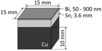
As shown in Fig. 1, the specimen used in this study com-prised a 15 mm × 15 mm × 5 mm block cut from 99.9% tin
ingot. This block was bonded to a copper block for the conve-nience of the tensile test of joints. To remove the processing layer, the faying surface of the tin (15 mm × 15 mm) was ground on emery paper and finished by electrolytic polishing in a solution containing 5% perchloric acid in 10% ethyl gly-col monobutyl ether and 85% ethyl alcohol. The surface roughness Ra was 0.33 μm. The filler metal was prepared by depositing Bi on the faying surface of Sn up to prescribed thickness (50~900 nm) by using vacuum deposition equip-ment (JEOL JEE-4X, Japan). The liquid phase diffusion bonding was carried out at bonding temperatures (T) ranging from 413 to 463 K in a vacuum chamber. The bonding pres-sure and bonding time were fixed at 7 MPa and 1.8 ks, re-spectively. The bonding pressure was applied until the bond-ing time ended before heatbond-ing the sample. The heatbond-ing rate was fixed at 0.35 K/s.
After liquid phase diffusion bonding, the specimen was cut into three pieces for the tensile test and metallographic obser-vation of bonded interface. Subsequently, the surface (trans-verse section) were prepared by grinding and polishing, after which they were inspected with scanning electron microscope (SEM: Shimadzu SSX-500, Japan) and energy dispersive X-ray analysis (EDX: Shimadzu SEDX-500, Japan). The specimen for the tensile test was cut from a bonded joint to give a sectional area of 3 mm × 3 mm. The tensile test was carried out along a direction vertical to the bonded interface at room temperature and a displacement speed of 0.017 mm・s−1. The interfacial hardness measured at load of 0.098 N by using micro-Vickers hardness tester (MVK-H1, *1
Corresponding author, E-mail: [email protected] *2
Present address: Canon Electronics Inc., Tokyo 105–0011, Japan
[image:1.595.340.513.309.395.2]Japan).
3. Experimental Results
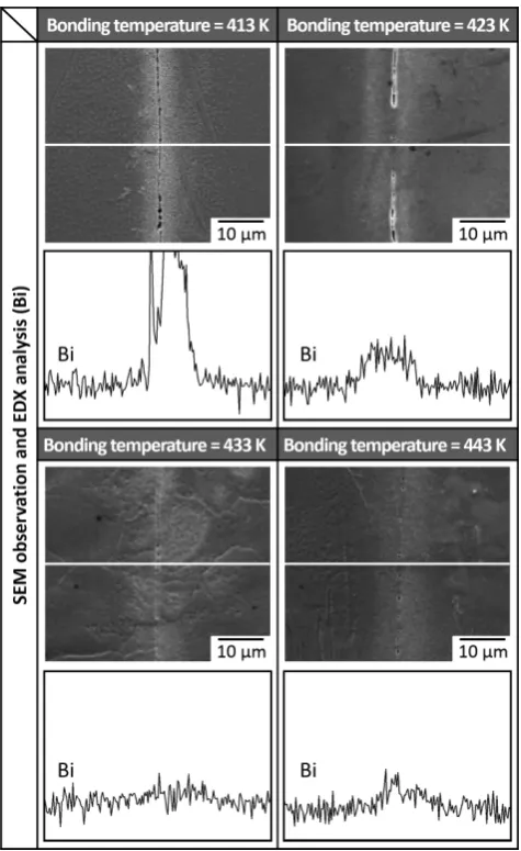
3.1 Effect of application of filler metal on bond strength To examine the influence of the filler metal thickness on the tensile strength of the joint, tensile test were performed after liquid phase diffusion bonding was carried out at filler thickness of 50~900 nm at a fixed bonding temperature of 433 K. The relationship between the filler thickness and ten-sile strength is shown in Fig. 2, and SEM images of the joint interfaces and results of the EDX analysis (Bi) are shown in Fig. 3. The joint with the highest strength was obtained when the filler thickness was 600 nm. When the filler thickness was 50 nm, line shaped gaps which width is about 10 μm were observed and Bi concentrated area was not detected. Also, when the filler metal thickness was 900 nm, gaps were mere-ly observed but the white colored particles which diameter are about 2 μm were observed. And Bi concentrated area which thickness is about 10 μm was detected. These observa-tions suggested that when the filler thickness is thin, the irreg-ularity of the faying surface is not filled; and when the thick-ness is thick, fragile Bi primary crystal remained at the joint
interface. For these reasons, it was determined that the best Bi filler thickness was 600 nm.
[image:2.595.68.269.366.512.2]Figure 4 presents the relationship between the bonding temperature and the tensile strength of the joints. In addition, the degree of deformation (D (%)) calculated with D (%) = (1- height of Sn part after joining / height of Sn part before bonding) × 100 was described in parallel in Fig. 4. Here, the height of Sn part is height of Sn blocks in the direction where the bonding pressure was applied which includes the filler metal placed between Sn blocks. And to illustrate the effect of the filler metal, the results for a joint without filler metal are also shown. Although the tensile strength increased with bonding temperature independently of the filler metal, the tensile strength approached the base-metal strength at a bond-ing temperature about 20 K or more lower than that for the joint without filler metal. Moreover, fractures of the base-met-al in the joint occurred under the condition of T = 443 K with filler metal, but the joint without filler metal fractured at the joint interface at less than 463 K. And it was revealed that a high strength joint was provided from low degree of deforma-tion by applying filler metal.
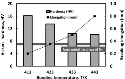
Figure 5 presents the relationship between the bonding temperature and breaking elongation with Vickers hardness around joint interface. With a rise in bonding temperature, the hardness decreased although the hardness was higher than that of base-metal of Sn. In addition, the breaking elongation
Fig. 2 Relation between tensile strength and filler thickness bonded at 433 K and 7 MPa.
Fig. 3 SEM micrographs and EDX analysis results of the bonded interfaces bonded at 433 K and 7 MPa with filler metal of 50 and 900 nm.
Fig. 4 Effect of filler metal on the relation between tensile strength and bonding temperature. The bonding pressure and time for all joints were 7 MPa and 1.8 ks, respectively.
[image:2.595.313.542.404.562.2] [image:2.595.49.289.567.762.2] [image:2.595.319.535.625.761.2]of Sn has increased as the hardness decreases. Therefore, it is inferred that the reason which the joint bonded at 413 K broke for brittleness is because interfacial Bi concentration was high. Actually, when the insert metal was applied up to 900 nm, large amount of Bi was detected around joint inter-face (see Fig. 3), and the breaking elongation was hardly ob-served.
The fractured surfaces of joints after tensile test are shown in Figs. 6 and 7. At a bonding temperature of 443 K without filler metal, breaking elongation was not shown and the frac-tured surface was smooth and was brittleness. Therefore, it is thought that the reason why the joint was low tensile strength is that a filmy oxide remained at the bonded interface. The examination result is clear from the TEM observation result that we carried out in the past23). At a bonding temperature of 463 K, a ductility breaking form was observed. And the frac-tured surface was formed by a minute dimple less than 1 μm in diameter. As for this factor, this is because intimate contact was achieved as a result that a filmy oxide changed into gran-ular oxide23).
On the other hand, at a bonding temperature of 413 K with filler metal, the fractured surface was brittleness and particles of about few μm in diameter were observed on the fractured surface. In addition, large amount of Bi were detected from the particles in comparison with other area. Here, the filler metal does not have irregularity before bonding because the filler metal applied by using vacuum deposition equipment. Therefore, it is thought that eutectic reaction between Sn and Bi started at the bond interface in the bonding temperature of 413 K more than eutectic temperature (411 K). And it is in-ferred that the particles were formed by primary crystal of Bi was crystallized. At a bonding temperature of 423 K, the frac-tured surface was rough as having cracked, and Bi was detect-ed by the entire surface. It is thought that this crack which was formed by a liquid phase having caused the solidification shrinkage. With a rise in bonding temperature, the brittle frac-ture mode such as cracks was not observed, and almost none of Bi was detected. At a bonding temperature of 443 K, the ductile fracture mode such as dimples came to be observed. Therefore, because the primary crystal of Bi disappears by isothermal solidification and the Bi concentration of the bonding interface decreased, and it is thought that a brittle fracture mode changed in a ductile fracture mode. In addition, because the intimate contact was achieved, it was suggested that a high tensile strength joint was provided.
3.2 Observation of bond interface
To clarify an application effect of Bi filler metal on interfa-cial microstructure, interfainterfa-cial observation was performed by using SEM. In case where the filler metal was not applied as shown in Fig. 8, a linear bond line was clearly observed and the intimate contact was achieved at a bonding temperature of 443 K. At a bonding temperature of 463 K, grain boundary moved from bond line up to around 2 μm. Using a self-diffu-sion coefficient (D = 6.2 × 10⁻¹⁶ m2・s−1) of the Sn at the Fig. 6 SEM micrographs of the fractured surfaces of joints after tensile test
(without filler metal).
Fig. 8 SEM micrographs of the bonded interfaces (without filler metal). Fig. 7 SEM micrographs and EDX analysis results of the fractured surfaces
[image:3.595.47.290.65.181.2] [image:3.595.308.546.68.472.2] [image:3.595.307.548.524.637.2]bonding temperature of 463 K, the movement distance of the grain boundary are estimated from the following expression:
d2 =2Dt (1)
where d is the movement distance of the grain boundary (m) and t is the bonding time in this study (1.8 ks). The calcula-tion result became 1.5 μm and almost accorded with an actual value. Therefore, this movement of the grain boundary was shown to depend on self-diffusion of Sn.
[image:4.595.308.546.68.456.2]The grain boundary movement is disturbed by oxide at the bond interface. However, it is known to come to be able to move a grain boundary with a decrease in distribution density of oxide. Therefore, at the bonding temperature of 463 K, it is expected easily that a distribution form of oxide varied from a filmy oxide into granular oxides. Actually, as shown in Fig. 9, the state that a grain boundary at a bonded interface escaped from an oxide particle was observed. For this reason, it is understood that the joint came to break ductility and high tensile strength joint came to provided. Actually, a ductili-ty-like break form was observed on the fractured surface after the tensile test.
On the other hand, as shown in Fig. 10, at a bonding tem-perature of 413 K with filler metal, non-contact area were observed at the bond interface. Therefore, it was suggested that the reason why a brittleness-like break form was ob-served was because non-coherence domain by the solidifica-tion cracking existed. With a rise in bonding temperature, non-contact area was decreased. As a result of EDX analysis, highly-concentrated Bi was detected from the bond interface. However, quantity of detection largely decreased when the bonding temperature was raised to 423 K or more. Therefore, it is understood that the reason why the tensile strengths in-creased from low bonding temperature was that an adherence of the bond surface by the liquid phase formation. As for the time to complete isothermal solidification, it is estimated for about 68 ks by using a self-diffusion coefficient (D = 1.8 × 10⁻¹⁶ m2・s−1) of the Sn at the bonding temperature of 443 K. However, in this study, it is observed to have already complet-ed isothermal solidification at the bonding temperature of 443 K. From a SEM image and EDX analysis result in Fig. 11, it is revealed that this reason is because a melt which was formed by a eutectic reaction was discharged to the
cir-cumference of the bonded interface. As a result of these, dif-fusing capacity to Sn basemetal of Bi decreases, and it is thought that the joint was able to obtain a high ductility. In addition, when the filler metal was applied, grain boundary movement was not observed in all bonding temperature. As for this cause, it is guessed that self-diffusion distance of Sn is around 0.8 μm at the bonding temperature of 443 K.
4. Conclusions
The conclusions of this study are summarized as follows. Fig. 10 SEM micrographs and EDX analysis results of the bonded
interfac-es (with filler metal).
Fig. 11 SEM micrograph and EDX analysis result of an edge of a bonded interface (with filler metal, T = 443 K).
[image:4.595.63.277.69.233.2] [image:4.595.306.549.514.609.2](1) The application of Bi filler has decreased bonding tem-perature by 20 K or more which the bonded joints obtained bond strength comparable to the base metal of Sn.
(2) With a drop of the Bi concentration of the bonding in-terface, braking elongation increased and the failure mode changed from brittle to ductile.
(3) It was suggested that the application of Bi filler greatly contributed to interfacial coherence in the early stage of the bonding process.
Acknowledgement
This work was supported by Grant-in-Aid for Young Scien-tists (B) (26820124) from Japan Society for the Promotion of Science (JSPS).
REFERENCES
1) Y. Sun, Y. Luo and X. Wang: J. Mater. Process. Technol. 212 (2012) 1331–1337.
2) H. Zhou and G. Liu: Meas. 45 (2012) 1414–1423.
3) Z. Xu, L. Ma, J. Yan, S. Yang and S. Du: Composites: Part A 43 (2012) 407–414.
4) Z. Ma, W. Zhao, J. Yan and D. Li: Ultrason. Sonochem. 18 (2011) 1062–1067.
5) S. Murali, N. Srikanth and C.J. Vath III: Mater. Charact. 50 (2003) 39–50.
6) Y. Luo, Z. Zhang, X. Wang and Y. Zheng: Microelectron. Eng. 87
(2010) 2429–2436.
7) M.M.R. Howlader and F. Zhang: Thin Solid Films 519 (2010) 804– 808.
8) Q. Wang, N. Hosoda, T. Itoh and T. Suga: Microelectron. Reliab. 43 (2003) 751–756.
9) M.M.R. Howlader, T. Kaga and T. Suga: Vacuum 84 (2010) 1334– 1340.
10) H. Takagi, R. Maeda and T. Suga: Sens. Actuators A Phys. 105 (2003) 98–102.
11) B. Bayram, O. Akar and T. Akin: Diamond Related Materials 19 (2010) 1431–1435.
12) M.M. Visser, S. Weichel, R. de Reus and A.B. Hanneborg: Sens. Actu-ators A Phys. 97–98 (2002) 434–440.
13) S. Koyama, Y. Aoki and I. Shohji: Mater. Trans. 51 (2010) 1759–1763. 14) N.P. Wikstrom, A.T. Egbewande and O.A. Ojo: J. Alloy. Compd. 460
(2008) 379–385.
15) K. Tokoro, N.P. Wikstrom, O.A. Ojo and M.C. Chaturvedi: Mater. Sci. Eng. A 477 (2008) 311–318.
16) T.C. Illingworth, I.O. Golosnoy and T.W. Clyne: Mater. Sci. Eng. A 445–446 (2007) 493–500.
17) M. Mazar Atabaki and A. Talebi Hanzaei: Mater. Charact. 61 (2010) 982–991.
18) K.O. Cooke, T.I. Khan and G.D. Oliver: Mater. Des. 33 (2012) 469– 475.
19) H. Nami, A. Halvaee and H. Adgi: Mater. Des. 32 (2011) 3957–3965. 20) M.S. Kenevisi and S.M. Mousavi Khoie: Mater. Des. 38 (2012) 19–25. 21) S. Koyama, T. Isaka and I. Shohji: Journal of The Japan Institute of
Electronics Packaging 14 (2011) 377–381.
22) S. Koyama, S.K. Ting, Y. Aoki and I. Shohji: Transactions of The Japan Institute of Electronics Packaging 6 (2013) 93–98.