Kinetics of Reactive Diffusion in the (Sn
Cu)
/
Ni System at Solid-State Temperatures
Misako Nakayama
1,+1and Masanori Kajihara
2,+21Graduate School, Tokyo Institute of Technology, Yokohama 226-8502, Japan
2Department of Materials Science and Engineering, Tokyo Institute of Technology, Yokohama 226-8502, Japan
The kinetics of the solid-state reactive diffusion in the (SnCu)/Ni system was experimentally observed to examine effects of addition of Cu into Sn on the growth behavior of compounds at the interconnection between the Sn-base solder and the multilayer Au/Ni/Cu conductor during energization heating. In this experiment, sandwich (SnCu)/Ni/(SnCu) diffusion couples with Cu concentrations ofy=0.010.03 were isothermally annealed at solid-state temperatures ofT=453473 K for various periods up to 1972 h, whereyis the mol fraction of Cu. After annealing, an intermetallic layer consisting of (Cu,Ni)6Sn5and Ni3Sn4was recognized between the SnCu and Ni specimens in the diffusion couple. The total thickness of the intermetallic layer is proportional to a power function of the annealing time, and the exponent of the power function takes values of 0.370.44 atT=453 K and those of 0.630.69 atT=473 K. Thus, the growth of the intermetallic layer is controlled by boundary and volume diffusion atT=453 K. On the other hand, atT=473 K, interface reaction and interdiffusion contribute to the rate-controlling process of the intermetallic growth. The addition of Cu into Sn accelerates the intermetallic growth within the experimental annealing times. [doi:10.2320/matertrans.M2015059]
(Received February 12, 2015; Accepted March 30, 2015; Published May 15, 2015)
Keywords: reactive diffusion, metallization, solder, conductor, intermetallic compounds
1. Introduction
Due to high electrical conductivity, Cu-base alloys are widely used as conductor materials in the electronics industry. When the Cu-base conductor is interconnected with a Sn-base solder, Cu6Sn5 and Cu3Sn are formed at the
interconnection between the conductor and the solder during soldering and then gradually grow during energization heating at solid-state temperatures.111) Since the CuSn
compounds are brittle and possess high electrical resistivities, their growth deteriorates the mechanical and electrical properties of the interconnection. To inhibit the formation of the compounds, the Cu-base conductor is usually plated with a Ni layer. However, Ni is not sufficiently corrosion resistant. Hence, the Ni layer is plated with a Au or Pd layer to improve corrosion resistance.1215)
For the multilayer Au/Ni/Cu conductor with a thin Au layer, the Au layer quickly dissolves into a molten Sn-base solder during soldering, and then the Ni layer is contacted with the solder. As a consequence, the Ni layer is directly reacted with the solder during solid-state energization heating. The solid-state reactive diffusion in the Ni/Sn system was experimentally examined using sandwich Sn/ Ni/Sn diffusion couples prepared by a diffusion bonding technique in a previous study.16) In this experiment, the
diffusion couples were isothermally annealed at temperatures ofT=433473 K. At the interface in the annealed diffusion couple, a layer of Ni3Sn4 was observed atT=453473 K,
but granular particles of Ni3Sn4 were recognized at T=
433 K. The mean thickness of the Ni3Sn4layer is proportional
to a power function of the annealing time. The exponent of the power function is 0.46 and 0.41 at T=453 and 473 K, respectively. The exponent smaller than 0.5 indicates that the growth of Ni3Sn4 is controlled by boundary and volume
diffusion and grain growth occurs in Ni3Sn4. Although the
growth of Ni3Sn4may be accelerated by boundary diffusion,
the overall growth rate is smaller for Ni3Sn416) than for
Cu6Sn5and Cu3Sn.3,11)Consequently, the Ni layer works as a
barrier against the reactive diffusion at the interconnection between the Sn-base solder and the multilayer Au/Ni/Cu conductor with a thin Au layer during solid-state energization heating.
Since the price is much lower for Cu than for Ag, SnCu alloys are more preferentially used as a low-cost Pb-free solder than SnAg alloys. In the SnCu solder, small particles of Cu6Sn5 are dispersed in the Sn matrix. The dispersion of
Cu6Sn5in the solder may influence the kinetics of the reactive
diffusion between the Sn matrix and the Ni layer at the interconnection. Unfortunately, however, reliable information on such influence is rather limited. To examine this influence, the kinetics of the reactive diffusion in the (SnCu)/Ni system was experimentally observed at solid-state temper-atures of T=453473 K using sandwich (SnCu)/Ni/(Sn Cu) diffusion couples with Cu mol fractions of 0.010.03 in the present study.
2. Experimental
Binary SnCu alloys with Cu concentrations ofy=0.01, 0.02 and 0.03 were made as 25 g button ingots by argon arc melting from pure Sn and Cu with purities of 99.99 and 99.96%, respectively, whereyis the mol fraction of Cu. Plate specimens with a size of 12 mm©5 mm©2 mm were prepared by cold rolling and spark erosion from the button ingots. The plate specimens were isothermally heated in an oil bath with silicone oil at 473 K for 2 h, followed by water quenching. The two surfaces with an area of 12 mm©5 mm of each heated SnCu plate specimen were mechanically polished on # 800 emery paper. One of the two polished surfaces was again mechanically polished on # 15004000 emery papers until a depth of 100 µm and thenfinished using diamond with a diameter of 1 µm.
Sheet specimens with a size of 20 mm©7 mm©0.2 mm were cut from a pure Ni commercial sheet with dimensions of 300 mm©100 mm©0.2 mm and purity of 99.97%and then
+1Graduate Student, Tokyo Institute of Technology
+2Corresponding author, E-mail: kajihara@materia.titech.ac.jp
separately annealed in evacuated silica capsules at 1173 K for 2 h, followed by air cooling without breaking the capsules. The annealed sheet specimens were chemically polished in nitrohydrochloric acid for 60 s.
After chemical polishing, a Ni sheet specimen was immediately sandwiched between the finished surfaces of two freshly prepared SnCu plate specimens in ethanol by the technique used in a previous study.11) The sandwich (Sn Cu)/Ni/(SnCu) couples were completely dried and then heat treated for diffusion bonding in the oil bath for 69 and 44.5 h at 453 and 473 K, respectively. After the heat treatment, the diffusion couples were isothermally annealed at 453473 K for various times up to 1903 h. The summation of the heat-treating and annealing times is hereafter merely called the annealing time t, and the annealing temperature is denoted by T. The chemical composition of the SnCu alloy is described as SnyCu. The Sn0.01Cu, Sn0.02Cu and Sn0.03Cu alloys are designated alloys C1, C2 and C3, respectively, and the diffusion couples with alloys C1, C2 and C3 are called diffusion couples C1, C2 and C3, respectively. Cross-sections of the annealed diffusion couple were mechanically polished using diamond with diameters of 15, 3 and 1 µm, and then finished with an OP-S liquid manufactured by Struers Ltd. The microstructure of the cross-section was observed by differential interference contrast optical microscopy (DICOM). Concentrations of Sn, Cu and Ni in each phase on the cross-section were measured by electron probe microanalysis (EPMA) using pure Sn, Cu and Ni with purity of 99.99% as standard specimens under the following conditions: the accelerating voltage was 20 kV; the probe current was 5 nA; the analyzing crystal was poly-ethylene terephthalate (PET) for SnL¡and lithiumfluoride (LiF) for CuK¡ and NiK¡; and the chemical composition was evaluated by a standard ZAF correction technique.
3. Results and Discussion
3.1 Microstructure
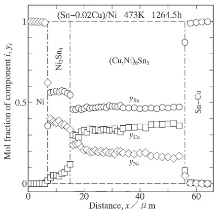
A typical DICOM image for the cross-section of diffusion couple C1 with T=473 K andt=787.5 h (2.84©106s) is shown in Fig. 1. In thisfigure, the top and bottom regions are the SnCu and Ni specimens, respectively. As can be seen, a layer with rather uniform thickness is formed at the original interface between the SnCu and Ni specimens. To identify each phase, concentration profiles of Sn, Cu and Ni were determined by EPMA along the direction normal to the original interface. A result for diffusion couple C2 with
T=473 K and t=1264.5 h (4.55©106s) is indicated in
Fig. 2. In Fig. 2, the ordinate and the abscissa show the mol fractionyiof componentiand the distancexmeasured from an arbitrary origin, respectively, and open circles, squares and rhombuses represent the mol fractions ySn, yCu and yNi,
respectively. As can be seen, the layer consists of two compounds. They are Ni3Sn4and (Cu,Ni)6Sn5on the Ni and
SnCu sides, respectively. The thickness is much smaller for Ni3Sn4than for (Cu,Ni)6Sn5. Furthermore, the concentration
of Cu in Ni3Sn4 is smaller than that of Ni in (Cu,Ni)6Sn5.
Hereafter, the (Cu,Ni)6Sn5+Ni3Sn4 two-phase layer is
merely called the intermetallic layer. If we observe the edge of diffusion couple on the cross-section, we can find the
location of the original (SnCu)/Ni interface. This observa-tion indicates that the intermetallic layer grows mainly into the SnCu specimen but slightly towards the Ni specimen. The EPMA measurement was conducted also for diffusion couples C1 and C3. Since the volume fraction of Ni3Sn4in
the intermetallic layer gradually decreases with increasing Cu concentration of the SnCu specimen, however, Ni3Sn4 is
rather invisible at shorter annealing times for diffusion couple C3.
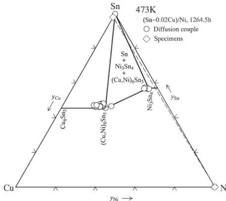
Recently, the phase equilibria at the Sn-rich corner in the ternary SnCuNi system were experimentally determined at solid-state temperatures in a previous study.17)The isothermal section at T=473 K of the phase diagram in this ternary system is shown in Fig. 3. As can be seen, a three-phase equilibrium of Sn+(Cu,Ni)6Sn5+Ni3Sn4 appears at this
temperature. According to the tie-triangle of this three-phase equilibrium, the solubilitysyCu6Sn5Ni of Ni in Cu6Sn5is 0.224,
and thatsyNi3Sn4Cu of Cu in Ni3Sn4is 0.046.17)Hence,syNi3Sn4Cu is
Fig. 1 Cross-sectional DICOM image of diffusion couple C1 annealed at
T=473 K fort=787.5 h (2.84©106s).
[image:2.595.312.541.69.247.2] [image:2.595.317.536.295.508.2]much smaller than syCu6Sn5Ni . Therefore, in Fig. 3, Cu6Sn5 is
described as (Cu,Ni)6Sn5, but Ni3Sn4 is merely expressed as
Ni3Sn4. The concentration profiles across the intermetallic
layer for diffusion couple C2 in Fig. 2 are plotted as open circles in Fig. 3. On the other hand, in Fig. 3, open rhombuses represent the chemical compositions of the Sn Cu and Ni specimens for diffusion couple C2. As can be seen, the open circles for (Cu,Ni)6Sn5and Ni3Sn4are located
in the neighborhood of the (Cu,Ni)6Sn5 and Ni3Sn4 corners,
respectively, of the Sn+(Cu,Ni)6Sn5+Ni3Sn4 tie-triangle.
Thus, the mol fraction yCu6Sn5Ni of Ni in (Cu,Ni)6Sn5 and
that yNi3Sn4Cu of Cu in Ni3Sn4 in Fig. 2 are close to the
solubilitiessyCu6Sn5Ni and syNi3Sn4Cu , respectively.
As indicated in Fig. 1, small particles of Cu6Sn5are thinly
dispersed in the Sn matrix of the SnCu specimen. Furthermore, the solubilities of Cu and Ni in the Sn matrix are negligible as shown in Fig. 3. Therefore, in the early stages of the reactive diffusion, a very thin Ni3Sn4 layer is
formed at the interface between the Sn matrix and the Ni specimen. As the annealing time increases, Cu atoms are transported from the Cu6Sn5 particles to the Ni3Sn4 layer
through the Sn matrix. The mol fraction yNi3Sn4Cu of Cu in Ni3Sn4is increased by the Cu-atoms transportation and then
reaches the solubility syNi3Sn4Cu . If yNi3Sn4Cu slightly exceeds syNi3Sn4
Cu , Ni3Sn4is transformed into (Cu,Ni)6Sn5. When local
equilibrium is realized at the interface between (Cu,Ni)6Sn5
and Ni3Sn4, yCu6Sn5Ni and yNi3Sn4Cu coincide with syCu6Sn5Ni and syNi3Sn4
Cu , respectively, at the interface. Since the (Cu,Ni)6Sn5/
Ni3Sn4 interface is produced by the transformation, it is not
so clearly distinguishable in cross-sectional DICOM images as shown in Fig. 1.
3.2 Growth behavior of intermetallic layer
From the cross-sectional DICOM images like Fig. 1, the areaAjof the intermetallic layer corresponding to the partial lengthwjof the original (SnCu)/Ni interface were measured for cross-section j. The sumsAand wwere obtained by the equations11)
A¼Xm j¼1
Aj (1a)
and
w¼Xm j¼1
wj (1b)
fromAjandwj, respectively, wherewj=422 µm andm²5. Using the values of A and w, the total thickness l of the intermetallic layer was evaluated at each annealing time tas follows:11)
l¼A
w: ð2Þ
The results of diffusion couples C1, C2 and C3 are plotted as open rhombuses, squares and circles, respectively, in Fig. 4, where the ordinate and the abscissa show the logarithms ofl
and t, respectively. In thisfigure, open triangles indicate the corresponding results of diffusion couple C0 reported in a
Fig. 3 Diffusion path for the concentration profiles shown in Fig. 2. The three-phase equilibrium of Sn+(Cu,Ni)6Sn5+Ni3Sn4in the ternary Sn CuNi system17)is also indicated as a tie-triangle.
(a)
(b)
[image:3.595.316.533.64.492.2] [image:3.595.52.280.69.272.2]previous study.16) Here, diffusion couple C0 stands for the Sn/Ni/Sn diffusion couple with y=0.16) Figure 4(a) and 4(b) indicates the results forT=453 and 473 K, respectively. As can be seen, the thicknesslmonotonically increases with increasing annealing time t. Furthermore, the plotted points for each diffusion couple lie well on a straight line. Consequently, l is expressed as a power function of t as follows.
l¼k tt 0
n
ð3Þ
Here, t0is unit time, 1 s. It is adopted to make the argument
t/t0of the power function dimensionless. The proportionality
coefficientkhas the same dimension as the thicknessl, and the exponent n is dimensionless. From the open symbols plotted in Fig. 4,kand n in eq. (3) were determined by the least-squares method as shown with various straight lines. The determined values are shown in Fig. 4. Since n varies depending on y, it is rather difficult to find a systematic relationship between k and y. Therefore, to estimate the composition dependence of the overall growth rate of the intermetallic layer, the thickness l6 at t=106s is plotted
againstyas open squares and circles forT=453 and 473 K, respectively, with error bars in Fig. 5. Hereafter, the error bar represents the standard error. For T=453473 K, l6
monotonically increases with increasing value of y at
y<0.1 but becomes rather insensitive to y at y>0.1. As previously mentioned, the intermetallic layer consists of Ni3Sn4 and (Cu,Ni)6Sn5. As the value of y increases,
the volume fraction of (Cu,Ni)6Sn5 increases, but that
of Ni3Sn4 decreases. According to the observations in
previous studies,11,16,17) the layer growth is much faster for (Cu,Ni)6Sn5 than for Ni3Sn4. Consequently, the overall
growth rate of the intermetallic layer monotonically increases with increasing value ofy. At larger values ofy, however, the volume fraction f is much greater for (Cu,Ni)6Sn5 than for
Ni3Sn4, and hence the dependence of f on y becomes less
remarkable. This is the reason why l6 monotonically
increases with increasing value ofyaty<0.1 but becomes rather insensitive toyaty>0.1.
3.3 Rate-controlling process of intermetallic growth
The values of natT=453 and 473 K are plotted against
y as open circles with error bars in Fig. 6(a) and 6(b), respectively. If the layer growth of the intermetallic layer is controlled by volume diffusion,nis equal to 0.5.1827)On the other hand, boundary diffusion may govern the layer growth at low temperatures where volume diffusion is frozen out. When the layer growth is controlled by boundary diffusion across the intermetallic layer and grain growth occurs in the intermetallic layer, n becomes smaller than 0.5.28) For y=
00.03 at T=453 K, n takes values of 0.370.46, and thus boundary diffusion mainly governs the layer growth. Such a rate-controlling process works also for y=0 at T=473 K. On the other hand,ntakes values of 0.630.69 fory=0.01 0.03 at T=473 K. If the interface reaction at the moving
Fig. 5 The thicknessl6att=106s versus the mol fractionyof Cu in the SnCu alloy shown as open squares and circles forT=453 and 473 K, respectively, with error bars. The corresponding results ofy=016)are also represented.
(a)
(b)
[image:4.595.61.283.65.275.2] [image:4.595.316.537.70.501.2]interface controls the layer growth, n is equivalent to unity.2937) As mentioned in Section 3.1, the intermetallic
layer grows predominantly into the SnCu specimen. Furthermore, (Cu,Ni)6Sn5 and Ni3Sn4 are located on the
SnCu and Ni sides, respectively. Thus, the valuesn=0.63 0.69 indicate that the layer growth is governed by the interface reaction at the migrating (SnCu)/(Cu,Ni)6Sn5
interface as well as the interdiffusion across the intermetallic layer. Such a mixed rate-controlling process of reactive diffusion has been observed for various metal systems. For instance, the reactive diffusion in the (CuSn)/Nb system was experimentally examined using diffusion couples con-sisting of CuSn alloys and Nb in previous studies.2931) In
these experiments, the diffusion couple was isothermally annealed at T=9231053 K. During annealing, a single-phase Nb3Sn layer is formed at the original (CuSn)/Nb
interface in the diffusion couple and grows mainly towards the Nb. Here, Nb3Sn is one of the most important
superconducting materials. According to the results in Fig. 5, the overall growth rate of the intermetallic layer and thus the migration rate of the (SnCu)/(Cu,Ni)6Sn5interface
is greater for y=0.010.03 than for y=0. For the fast interface migration, the interface reaction is a bottleneck for the overall layer growth, and hence n becomes greater than 0.5.36,37) Therefore, at T=473 K, n is greater than 0.5 for
y=0.010.03, thoughnis smaller than 0.5 fory=0. As the annealing temperature Tdecreases, the interdiffusion across the intermetallic layer becomes sluggish, and thus the interface reaction is no longer a bottleneck. Consequently, atT=453 K,nis smaller than 0.5 not only fory=0 but also fory=0.010.03.
4. Conclusions
The solid-state reactive diffusion in the (SnCu)/Ni system was experimentally observed using the (SnCu)/ Ni/(SnCu) diffusion couples with Cu mol fractions ofy=
0.010.03. The diffusion couples were isothermally annealed in the temperature range ofT=453473 K for various times up to t=1972 h. During annealing, the (Cu,Ni)6Sn5+
Ni3Sn4 two-phase layer is formed at the original (SnCu)/
Ni interface in the diffusion couple. The total thickness of the two-phase layer is proportional to a power function of the annealing time. The exponent of the power function takes vales of 0.370.44 at T=453 K and those of 0.630.69 at
T=473 K. Therefore, atT=453 K, the growth of the two-phase layer is controlled by boundary and volume diffusion. In contrast, at T=473 K, interface reaction as well as interdiffusion contributes to the rate-controlling process of the layer growth. The overall growth of the two-phase layer is accelerated by the addition of Cu into Sn.
Acknowledgements
The present study was supported by the Iketani Science and Technology Foundation in Japan. The study was also partially supported by a Grant-in-Aid for Scientific Research from the Ministry of Education, Culture, Sports, Science and Technology of Japan.
REFERENCES
1) L. Zakraysek: Welding Res. Suppl.Nov.(1972) 536541. 2) K. N. Tu:Acta Metall.21(1973) 347354.
3) M. Onishi and H. Fujibuchi: Trans. JIM16(1975) 539547. 4) H. N. Keller:IEEE Trans. Compon. Hybrids Manuf. Tech.2(1979)
180195.
5) H. N. Keller and J. M. Morabito:Surf. Interface Anal.3(1981) 1622.
6) J. O. G. Parent, D. D. L. Chung and I. M. Bernstein:J. Mater. Sci.23
(1988) 25642572.
7) A. J. Sunwoo, J. W. Morris, Jr. and G. K. Lucey, Jr.:Metall. Trans. A
23(1992) 13231332.
8) P. T. Vianco, P. F. Hlava and A. L. Kilgo:J. Electr. Mater.23(1994) 583594.
9) D. R. Frear and P. T. Vianco:Metall. Trans. A25(1994) 15091523.
10) S. Choi, T. R. Bieler, J. P. Lucas and K. N. Subramanian:J. Electr. Mater.28(1999) 12091215.
11) T. Takenaka, S. Kano, M. Kajihara, N. Kurokawa and K. Sakamoto:
Mater. Sci. Eng. A396(2005) 115123.
12) C. Wright:IEEE Trans. Parts Hybrids Packag.13(1977) 202207.
13) H. N. Keller:IEEE Trans. Compon. Hybrids Manuf. Tech.5(1982) 408419.
14) E. I.-B. Hannech and C. R. Hall:Mater. Sci. Tech.8(1992) 817824.
15) G. Ghosh:Acta Mater.48(2000) 37193738.
16) M. Mita, M. Kajihara, N. Kurokawa and K. Sakamoto:Mater. Sci. Eng. A403(2005) 269275.
17) W. Shinmei: Master Thesis, Tokyo Institute of Technology, (2013). 18) M. Kajihara:Acta Mater.52(2004) 11931200.
19) M. Kajihara:Mater. Sci. Eng. A403(2005) 234240.
20) M. Kajihara:Defect Diffusion Forum249(2006) 9196.
21) M. Kajihara:Mater. Trans.46(2005) 21422149.
22) M. Kajihara:Mater. Trans.47(2006) 14801484.
23) M. Kajihara and T. Yamashina:J. Mater. Sci.42(2007) 24322442.
24) M. Kajihara:Mater. Trans.49(2008) 715722.
25) M. Kajihara:J. Mater. Sci.44(2009) 21092118.
26) M. Kajihara:Mater. Trans.51(2010) 12421248.
27) M. Kajihara:Mater. Trans.53(2012) 18961904.
28) A. Furuto and M. Kajihara:Mater. Trans.49(2008) 294303.
29) Y. Muranishi and M. Kajihara:Mater. Sci. Eng. A404(2005) 3341.
30) T. Hayase and M. Kajihara:Mater. Sci. Eng. A433(2006) 8389.
31) K. Mikami and M. Kajihara:J. Mater. Sci.42(2007) 81788188.
32) M. Kajihara and Y. Tejima:J. Phys. Conf. Ser.165(2009) 012091.
33) Y. Tejima, S. Nakamura and M. Kajihara:J. Mater. Sci.45(2010) 919 928.
34) M. O, Y. Takamatsu and M. Kajihara:Mater. Trans.55(2014) 1058 1064.
35) M. Hashiba, K. Masui and M. Kajihara:Mater. Trans.56(2015) 3039.
36) Y. Yamamoto and M. Kajihara:Mater. Trans.42(2001) 17631770.