Interfacial Nano-Mechanical Properties of Copper Joints Bonded
with Silver Nanopaste near Room Temperature
Peng Peng
1,+, Peng He
2, Guisheng Zou
3, Lei Liu
3and Y. Norman Zhou
1,2,31Centre for Advanced Materials Joining, University of Waterloo,
200 University Avenue West, Waterloo, ON, N2L 3G1, Canada
2State Key Laboratory of Advanced Welding and Joining, Harbin Institute of Technology,
92 West Dazhi Street, Harbin, 150001, China
3Department of Mechanical Engineering, Tsinghua University, Beijing, 100084, China
Sintering of nanomaterials at low temperatures has been demonstrated as an alternative forflexible electronic packaging. Silver nanowires were synthesized via polyol method and used asfiller material for bonding copper to copper near room temperature. The experimental results indicated that both silver-to-silver and copper-to-silver formed metallurgical bonds. The elastic modulus and nano-hardness of copper joints at the copper-silver interface were characterized using nanoindentation. A transition layer at the interface was observed and its thickness was determined. Sintered silverfiller material showed good elasticity both inside and out of the transition layer. [doi:10.2320/matertrans.MI201412]
(Received December 15, 2014; Accepted February 18, 2015; Published March 27, 2015)
Keywords: Interface, diffusion, hardness, electronic packaging, mechanical properties
1. Introduction
The interconnection of components with metallurgical bonds is a key requirement for micro/nano-electronic devices since conductive joints are needed in transistors,13) sensors,4,5) solar cells6,7) and display units.810) Commonly used lead-free soldering processes reach 200 to 300°C to obtain conductive joints,11,12) which severely restricts joining for heat-sensitive components in flexible electronic devices.13,14) After a decade of efforts, low temperature interconnection processes using metallic nanoparticle paste through thermal sintering have been demonstrated with different metal nanoparticles,1517) and appears to be a promising alternative for lead-free electronic packaging and flexible electronic interconnections.1821)Such sintered metal nanoparticles have good electrical/thermal conductivities which could benefit the electrical/thermal properties of joints for electronics. Recently, silver nanowire (Ag NW) paste was also used asfiller material to bond Copper (Cu) onto Cu or plastic substrates at room temperature.22)
Most recent studies regarding the mechanical properties of joints bonded with nanomaterials have been focused on the macro and/or micro scale and have explored variables such as bonding strength and fatigue properties of joints. To improve the bonding strength, many researchers have varied the bonding parameters (temperature, time, pressure) or size, shape and composition of the nanomaterials used. However, few have paid attention to near room temperature bonding processes and the nano-mechanical properties of the joints especially at the bonding interface to understand the under-lying mechanisms. Usually, the inter-diffusion of atoms at the interface after solid-state bonding at high temperature can form a thick transition layer because the diffusion rate is fast leading to a long diffusion length, producing layers that are easy to characterize by examining the phases using mi-croscopy and the hardness through micro-hardness testing at the interface. In the case of low temperature bonding with
nanomaterials, examination might be more difficult due to the very thin transition layer in consequence of the moderate diffusion and restricted diffusion length. Therefore, the mechanical properties of the bonded interface formed at low temperature are seldom reported. In this paper, nanoindenta-tion was used to characterize the nano-mechanical properties of Cu joints bonded with Ag nanowire paste at the Cu-Ag interface. The elastic modulus and nano-hardness of the transition layer formed at low temperature were measured.
2. Experimental Procedure
All the chemicals and reagents were of analytical grade and used in the as received form without any purification. Ag NWs were synthesised using the modified polyol
meth-od.16,2224) Typically, 330 mg polyvinylpyrrolidone or PVP
((C6H9NO)n, K25, M.W.=24000, Alfa Aesar) and 12.5 mg silver chloride (AgCl, Alfa Aesar) were mixed with 40 mL ethylene glycol (EG, Fisher Chemical) in a round-bottom flask. The mixture was heated to between 160 and 170°C. Then, 110 mg silver nitrate was dissolved in 10 mL ethylene glycol liquid and added into the mixed solution while stirring vigorously and continuing the reaction conditions for 4 h. The Ag NWs were condensed by centrifugation at 4000 rpm using a 50 mL centrifuge pipe. The clean supernatants were removed from the centrifuge pipes using a pipette resulting in highly concentrated Ag NW pastes.
Afield-emission scanning electron microscope (FE-SEM, Zeiss LEO 1530 Gemini, Germany) was used to study the microstructure of interfaces and fracture surfaces of bonded samples. An oscillating knife (DIATOM, Ultrasonic) in ultramicrotome was used to section the interfaces of low-temperature bonded samples produced with Ag nanopaste. Thin slices of 100 nm thickness were observed using high resolution transmission electron microscopy (HRTEM, JEOL 2010F).
The joints were made by pre-assembling pairs of separated Cu plates (99.9% purity, Arcor Electronics, Northbrook, IL) with a gap (³1 mm) between them. Ag nanopaste was then +Corresponding author, E-mail: p5peng@uwaterloo.ca
Special Issue on Nanojoining and Microjoining II
filled into the gap in a drop-wise manner to bond them by baking at 60°C for 1 h in air. The cross sections of bonded samples were mounted using epoxy resin and polished with 0.25 µm diamond paste to get a flat Cu-Ag interface. It is worth noting that the work-hardened layer created by mechanical polishing in this comparative study of mechanical properties of Cu and Ag surfaces finished under the same saturation could be negligible. The mechanical properties of the Cu-Ag interfaces were tested with a depth-sensing nanoindenter (Hysitron Triboindenter) equipped with a Berkovich tip. The tip was calibrated on fused silica. Indentations were performed on the mechanically polished flat surfaces in a load controlled mode. All nanoindentation experiments were performed using a constant loading rate of 60 µN/s, with loads of 600 µN.
3. Results and Discussion
The as-synthesized Ag nanopaste was in greyish color, as shown in Fig. 1(a). We have demonstrated that the organic content in the paste could be removed simply by washing with deionized water. After three washing cycles, the organic content was only 0.4 mass%22) and would not be further reduced significantly with increasing washing cycles. Ag nanopaste washed three times was used in this research. The SEM examination showed that Ag NWs had a length of about 20 µm and thickness around 90 nm, see Fig. 1(b). This Ag nanopaste could bond Cu with different substrates (such as Cu plate, Ag or Au coated plastics or even ITO-PET22)) at room temperature. Here, two Cu plates were bonded at 60°C as shown in Fig. 1(c).
The bonded Cu-Ag interface was sliced with an oscillating knife in an ultramicrotome and observed under TEM. The Ag
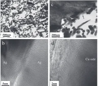
filler material was porous because no external pressure was employed during bonding (or sintering) of the Ag nanopaste, see Fig. 2(a). As shown in Fig. 2(b) neighbouring NW were interconnected at atomic level. Ag NWs were also bonded onto Cu substrate surface, see Fig. 2(c); meanwhile, some amorphous nanoparticles were observed very near to the Cu substrate as well as on the adjacent NWs as arrows indicated. These nanoparticles were confirmed as CuO when water-based Ag NW (PVP coated) paste was used.22,25)It is also worth mentioning that CuO nanoparticles existing at the interface could act as a co-bonding material which would be reduced when the bonding temperature increased and be changed into pure Cu if the bonding temperature was raised to 150°C.22)Figure 2(d) shows the typical HRTEM image of a Cu-Ag interface suggesting an atomic level bonding.
Fig. 1 Optical (a) and SEM (b) images of Ag nanopaste; (c) Bonding of Cu at low temperature using Ag nanopaste.
500nm 200nm
5nm 2nm
a
c
b
d
Ag
Ag
Cu side
Ag side
[image:2.595.307.544.70.230.2] [image:2.595.142.455.491.768.2]Consequently, these metallurgical bonds among Ag-to-Ag and Cu-to-Ag contribute to the good mechanical and electrical properties of joints bonded near room temperature as reported in our previous work.22)
To characterize the mechanical properties of Cu-Ag interfaces formed at low temperature, a bonded sample was mechanically polished followed by nanoindention testing across the interface from Cu to Ag side. Figure 3(a) shows the polished surface with an around 10 µm transition layer. The transition layer has also been observed at Cu-Ag interface formed at 150°C when Ag nanoparticle paste has been used.16) High magnification image (Fig. 3(b)) clearly displays that Cu and Ag has been bonded tightly except for a few voids along the interface. These voids (highlighted in cycle) were formed during the bonding process due to the incomplete wettability of water-based Ag nanopaste on the Cu surface. A thin dark layer with thickness of around 5 µm was seen on the Ag side as pointed out by solid arrows which might indicate the presence of CuO nanoparticles near to the Cu surface as mentioned above. The nanoindentation testing was conducted from Cu to Ag side as indicated by the dashed arrow in Fig. 3(b).
Measured elastic modulus, E, was obtained from the recorded reduced modulus,Er, in nanoindentation according to the Oliver and Pharr method2628)using eq. (1),
1 Er ¼
1¯2
E þ
1¯2 i
Ei ð1Þ
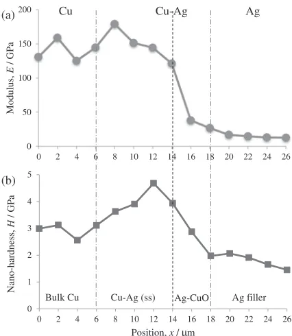
where, ¯ is the Poisson’s ratio of silver (¯=0.37);2931) ¯ i refers to the Poisson’s ratio of the indenter, here it is diamond (¯i=0.07);Eiis modulus of indenter (Ei=1141 GPa).26,28,32) In Fig. 4(a), it is found that the modulus stays at around 140 GPa when position x is 014 µm and then decreases dramatically when x is larger than 14 µm. The sintered porous Agfiller material away from Cu surface has modulus of 13 GPa. This low elastic modulus of sintered porous Ag filler material is very close to the modulus of 8 GPa for polyimide based substrates33)and 11 GPa for PET/glassfiber substrates.34) The relative density could be calculated using measured modulus according to the relation of µ/µbulk= (E/Ebulk)1/2.35) Here, the measured modulus of bulk poly-crystalline Ag (assuming 100% dense) was 95.1«4.4 GPa. Therefore, the porosity of sintered porous Ag filler material was around 62%. The high porosity was due to the low bonding temperature without external bonding pressure. The
high porosity and the close elastic modulus between the Ag porous filler material and widely used flexible substrates make them mechanically compatible during deformation. This matching will help to relieve the thermomechanical stress by taking advantage of the porous structure36) in practical applications. The nano-hardness profile is plotted in Fig. 4(b). Cu substrate had a measured nano-hardness of 3 GPa. It increased while the testing entered into the transition layer at the Cu-Ag interface. The maximum value was 4.7 GPa (when position x was 12 µm) which is in agreement with the hardness of Cu-Ag nanocomposite film when Cu concentration is close to 80 at%.37)Then, the nano-hardness dropped moving toward the Ag side. Starting from a positionxof 18 µm, it remained around 1.8 GPa suggesting the ending of the transition layer.
Considering both the modulus and nano-hardness results in Fig. 4, it could be speculated that the Cu-to-Ag transition occurred at around positionx=14 µm (as the dark dash line indicated) because of the significant drop of modulus attributed to the porous structure of Ag filler material. The thickness of transition layer was about 12 µm (the boundaries
Fig. 3 Low (a) and high (b) magnification SEM images at Cu-Ag interface after bonding.
0 1 2 3 4 5
0 2 4 6 8 10 12 14 16 18 20 22 24 26
Nano-hardness,
H
/G
P
a
Position, x/µm 0
50 100 150 200
0 2 4 6 8 10 12 14 16 18 20 22 24 26
Modulus,
E
/G
P
a
Cu Cu-Ag Ag
(a)
(b)
Bulk Cu Cu-Ag (ss) Ag-CuO Ag filler
[image:3.595.103.489.70.201.2] [image:3.595.320.533.250.495.2]are indicated with gray dash-dot lines). The maximum nano-hardness in the transition layer may be due to the Cu-Ag solid solution (ss) because a large amount of Ag atoms diffused into the Cu lattice. However, the Cu atoms were not able to diffuse far into the Ag because of the limited diffusion paths on the Ag side caused by the porous structure. Further, the diffusion coefficient of Cu is lower than that of Ag.38) The high nano-hardness of Ag near the Cu surface is attributed to the presence of CuO nanoparticles. With the amount of CuO in Ag reducing with increased distance away from the Cu surface, the nano-hardness decreases as well and remains stable eventually when no CuO nanoparticles exist in the Ag filler material.
Figure 5 shows the load-depth curves during nanoindenta-tion in the transinanoindenta-tion layer. It was found that the shapes of curves for the Cu side (position x=8 and 12 µm in Fig. 4) were similar. They had similar elastic regions as the dashed circle highlighted during loading and similar slopes of unloading. The test closer to the Ag side (when position x=12 µm) had a smaller maximum depth at peak load of 600 µN and smaller indentation depth after unloading than that of the one farther from the Ag (when positionx=8 µm). This is a sensible result because more Ag atoms in the Cu would restrain the slip and dislocation movement in crystals during deformation. This solid solution strengthening caused the increase of nano-hardness as discussed in Fig. 4(b). However, the curve of the Ag side (when positionx=16 µm) displayed a very different shape which also confirms that it belongs to a different material. Although this curve had the largest maximum depth of 69 nm when the load was 600 µN, it had fairly close indentation depth after unloading with the Cu-Ag solid solution at x=12 µm, suggesting it has good elasticity.
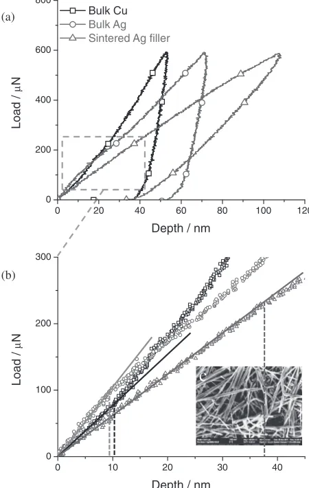
Comparing the nanoindentation load-depth curves of the Cu substrate and the sintered Ag filler material out of the transition layer, the maximum depth of Agfiller material was 108 nm with a load of 600 µN which was twice that of bulk Cu’s 53 nm although their the indentation depths after unloading were the same, see Fig. 6(a). Therefore, a large fraction of the deformation of Ag filler material was elastic deformation rather than plastic. It is worth mentioning that the maximum indentation depth of Ag filler material out of
the transition layer is larger (69 nm as shown in Fig. 5) than that of the Ag in the transition layer, which is attributed to the presence in the latter of CuO nanoparticles which act as a high hardness reinforcing material. Bulk Ag has a similar curve as bulk Cu but with larger plastic deformation. Figure 6(b) is the enlarged plots of the initial stages of the loading curves. It clearly shows that the elastic regions of the bulk Cu and Ag were fairly small (ended at around depth of 10 nm) while the Ag filler’s elastic region was delayed to around 37 nm. This also confirmed the good elasticity of Ag filler material as mentioned above. Both this long elastic region and the largest maximum depth during loading suggest that Ag filler material could store and absorb more strain energy compared with bulk Cu and Ag because of its porous structure after bonding as shown in Fig. 6(c). Consequently, by varying the porous structure of this Ag material, it could be used on different substrates forflexible electronics.39)
4. Conclusions
In summary, the microstructure and nano-mechanical properties of Cu joints bonded with Ag nanopaste at low temperature were studied. The results showed that Ag
0 20 40 60 80
0 200 400 600 800
Load /
µ
N
Depth / nm
Position x= 8 µm
Position x= 12µm
Position x= 16µm
Fig. 5 Load-depth curves at different positions of transition layer.
0 100 200 300
Load /
µ
N
Depth / nm
0 10 20 30 40
0 20 40 60 80 100 120 0
200 400 600 800
Load /
µ
N
Depth / nm Bulk Cu
Bulk Ag
Sintered Ag filler
(a)
(b)
c
[image:4.595.313.538.75.430.2]nanopaste could be used as filler material for Cu to Cu bonding at 60°C near room temperature without external bonding pressure. Both Ag-Ag and Cu-Ag formed metal-lurgical bonds. The Ag filler material after bonding was porous with high porosity of 62% and low elastic modulus of 13 GPa. The high porosity could help to relieve the thermomechanical stress of bonded joints during service. The low modulus would also benefit theflexible electronics during deformation due to its compatible mechanical proper-ties with widely used plastic substrates. A thin transition layer with a thickness of 12 µm at Cu-Ag interface was determined and its maximum hardness was 4.7 GPa. The nano-hardness of the transition layer exceeded the nano-nano-hardness values for Cu substrate and sintered Agfiller material. At the interface, the high nano-hardness on the Cu side was due to solution hardening in consequence of the diffusion of Ag atoms into Cu, while the presence of CuO nanoparticles on the Ag side contributed to enhancement of its nano-hardness. In the transition layer, diffusion of Ag into Cu and the existence of CuO in the Ag filler material restrained their plastic deformation, respectively. Out of the transition layer, Agfiller material showed large elasticity during deformation because of the porous structure which could absorb more strain energy and ultimately benefitflexible electronics.
Acknowledgments
The authors would like to acknowledge Dr. Yuquan Ding from the Department of Mechanical and Mechatronics Engineering at the University of Waterloo for nanoindenter operation. Appreciation is also expressed to Prof. Scott Lawson from the Centre for Advanced Materials Joining, University of Waterloo for useful discussions.
REFERENCES
1) J. H. Ahn, H. S. Kim, K. J. Lee, S. Jeon, S. J. Kang, Y. G. Sun, R. G. Nuzzo and J. A. Rogers:Science314(2006) 17541757.
2) T. Sekitani, U. Zschieschang, H. Klauk and T. Someya:Nat. Mater.9 (2010) 10151022.
3) D. M. Sun, M. Y. Timmermans, Y. Tian, A. G. Nasibulin, E. I. Kauppinen, S. Kishimoto, T. Mizutani and Y. Ohno:Nat. Nanotechnol. 6(2011) 156161.
4) B. Yoon, D. Y. Ham, O. Yarimaga, H. An, C. W. Lee and J. M. Kim:
Adv. Mater.23(2011) 54925497.
5) T. Someya, Y. Kato, T. Sekitani, S. Iba, Y. Noguchi, Y. Murase, H. Kawaguchi and T. Sakurai:PNAS102(2005) 1232112325.
6) T. S. van der Poll, J. A. Love, T. Q. Nguyen and G. C. Bazan:Adv. Mater.24(2012) 36463649.
7) W. B. Yang, H. S. Duan, B. Bob, H. P. Zhou, B. Lei, C. H. Chung, S. H. Li, W. W. Hou and Y. Yang:Adv. Mater.24(2012) 63236329.
8) A. Perumal, M. Frobel, S. Gorantla, T. Gemming, B. Lussem, J. Eckert
and K. Leo:Adv. Funct. Mater.22(2012) 210217.
9) Q. Wang, Y. T. Tao, X. F. Qiao, J. S. Chen, D. G. Ma, C. L. Yang and J. G. Qin:Adv. Funct. Mater.21(2011) 16811686.
10) Y. Jin, J. Feng, X. L. Zhang, Y. G. Bi, Y. Bai, L. Chen, T. Lan, Y. F. Liu, Q. D. Chen and H. B. Sun:Adv. Mater.24(2012) 11871191.
11) Y. Li, K. S. Moon and C. P. Wong:Science308(2005) 14191420.
12) J. P. Coughlin, J. J. Williams, G. A. Crawford and N. Chawla:Metall. Mater. Trans. A Phys. Metall. Mater. Sci.40(2009) 176184.
13) Y. Lu, J. Y. Huang, C. Wang, S. H. Sun and J. Lou:Nat. Nanotechnol.5 (2010) 218224.
14) L. B. Hu, M. Pasta, F. La Mantia, L. F. Cui, S. Jeong, H. D. Deshazer, J. W. Choi, S. M. Han and Y. Cui:Nano Lett.10(2010) 708714.
15) E. Ide, S. Angata, A. Hirose and K. F. Kobayashi:Acta. Mater.53 (2005) 23852393.
16) P. Peng, A. M. Hu, B. X. Zhao, A. P. Gerlich and Y. N. Zhou:J. Mater. Sci.47(2012) 68016811.
17) T. Bakhishev and V. Subramanian:J. Electron. Mater.38(2009) 2720 2725.
18) A. Hu, J. Guo, H. Alarifi, G. Patane, Y. Zhou, G. Compagnini and C. Xu:Appl. Phys. Lett.97(2010) 153117.
19) H. Alarifi, A. M. Hu, M. Yavuz and Y. N. Zhou:J. Electron. Mater.40 (2011) 13941402.
20) C. Yang, W. Lin, Z. Y. Li, R. W. Zhang, H. R. Wen, B. Gao, G. H. Chen, P. Gao, M. M. F. Yuen and C. P. Wong:Adv. Funct. Mater.21 (2011) 45824588.
21) Z. Li, R. Zhang, K. S. Moon, Y. Liu, K. Hansen, T. Le and C. Wong:
Adv. Funct. Mater.23(2013) 14591465.
22) P. Peng, A. M. Hu, H. Huang, A. P. Gerlich, B. X. Zhao and Y. N. Zhou:J. Mater. Chem.22(2012) 1299713001.
23) Y. Sun, B. Mayers, T. Herricks and Y. Xia:Nano Lett.3(2003) 955 960.
24) Y. Sun, Y. Yin, B. T. Mayers, T. Herricks and Y. Xia:Chem. Mater.14 (2002) 47364745.
25) P. Peng, H. Huang, A. M. Hu, A. P. Gerlich and Y. N. Zhou:J. Mater. Chem.22(2012) 1549515499.
26) W. C. Oliver and G. M. Pharr:J. Mater. Res.7(1992) 15641583.
27) W. C. Oliver and G. M. Pharr:J. Mater. Res.19(2004) 320.
28) X. Li and B. Bhushan:Mater. Charact.48(2002) 1136.
29) S. Cuenot, C. Frétigny, S. Demoustier-Champagne and B. Nysten:
Phys. Rev. B69(2004) 165410.
30) L. Bonacina, A. Callegari, C. Bonati, F. van Mourik and M. Chergui:
Nano Lett.6(2006) 710.
31) G. Perrin:J. Phys. Chem. Solids62(2001) 20912094.
32) X. Li, H. Gao, C. J. Murphy and K. Caswell:Nano Lett.3(2003) 14951498.
33) R. Li and J. Jiao: Proceedings-Spie the International Society for Optical Engineering, International Society for Optical Engineering, 1999, 2000, 068073.
34) D. Bhattacharyya, P. Maitrot and S. Fakirov:Express Polym. Lett.3 (2009) 525532.
35) R. Dou, B. Xu and B. Derby:Scr. Mater.63(2010) 308311.
36) G. Bai: Doctoral Thesis, Virginia Polytechnic Institute and State University, (2005).
37) S. Zghal, R. Twesten, F. Wu and P. Bellon: Acta Mater.50(2002) 47114726.
38) B. Dyson, T. Anthony and D. Turnbull:J. Appl. Phys.37(1966) 2370 2374.