Effects of Post-Plating Reflow on Changes in Crystal Grain Size
of Sn-2 mass%Bi Alloy Plating with Thermal Cycling Treatment
Noriyuki Kuwano
1;2, Atsushi Jinnouchi
2, Sadanori Horikami
2,
Naruyoshi Hirokado
2and Harini Sosiati
31Art, Science and Technology Center for Cooperative Research, Kyushu University, Kasuga 816-8580, Japan 2Department of Applied Science for Electronics and Materials, Kyushu University, Kasuga 816-8580, Japan 3The Research Laboratory for High Voltage Electron Microscopy, Kyushu University, Fukuoka 819-0395, Japan
Changes in the grain size of tin (Sn) crystals associated with a thermal cycling treatment were investigated for layers of Sn-2 mass%Bi electroplated on Fe-42Ni substrates in order to clarify the effects of post-plating reflow. Morphology of plated surface was observed by scanning electron microscopy (SEM) and scanning ion microscopy (SIM), and the Sn-grains were observed by electron beam back scattered diffraction (EBSD). Microstructures were also analyzed with a transmission electron microscope (TEM) in order to investigate the process of whisker formation. It was found that the Sn grains in Sn-Bi specimen are smaller than those in pure Sn specimen at the initial state of as-plating, after the reflow treatment and after the thermal cycling treatment of 1500 cycles. On the Sn-Bi specimen without a reflow treatment, short whiskers had grown after 100 cycles of thermal cycling treatment, but on those with the reflow treatment, relatively-long whiskers were formed after 500 cycles. The grain sizes increase temporarily after the reflow treatment and also after the very early stage of thermal cycling treatment, but gradually decreased with the thermal cycling treatment. The phenomenon is explained by the ‘‘deformation and recrystallization’’ effects of the thermal cycling treatment. [doi:10.2320/matertrans.MJ201021]
(Received April 28, 2010; Accepted August 2, 2010; Published September 25, 2010)
Keywords: tin whisker, electron microscopy, tin-bismuth, reflow, internal stress, grain size
1. Introduction
Due to restriction of hazardous substances for environ-mental concerns, lead (Pb)-free materials should be used in electronic devices and components. The need for using Pb-free solders and plating, such as pure-Sn and Pb-free Sn alloys, has invoked ‘‘spontaneous formation of whiskers’’ as a revival issue. There have been a lot of investigations on the origin of whisker formation so far.1,2) It was believed that the movement of dislocations plays a primary role in whisker formation (dislocation mechanism),3)but now a stress gradient inside the Sn layer and Sn-atom transport are thought to be the important factors for whiskers.4,5)Various attempts for mitigation against the whisker formation, e.g., alloying to be Sn-Ag and Sn-Bi and thermal processing such as a reflow treatment, have been made. However, the mechanism of whisker-growth has not been well understood and the complete prevention from whisker formation has not yet been established to date. In the present work, with focusing attention to the grain size of Sn crystals that is considered as one of the factors inducing whiskers,6)the changes in grain size with the thermal cycling treatment were investigated in order to clarify the effect of post-plating reflow treatment.
2. Experimental
Samples were prepared by electroplating a matte Sn-2 mass%Bi film about 10mm thick with a methansulphonic acid (MSA) based commercial electroplating solution on a substrate of Fe-42 Ni. The current was 10 A/dm2 (1103
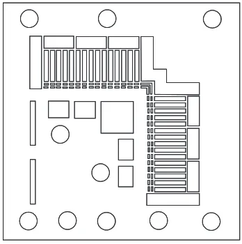
A/m2). The substrates for test-piece were specially designed for experimental examination to have components of comb-shaped leads. Figure 1 shows schematically a typical shape of the substrate. The sizes of substrate were3636mm2and 0.2 mm in thickness, and the width of leads was 0.3 mm.
Samples of a matte pure-Sn plating on the substrate were also prepared for reference. A reflow treatment at 260C was done for some of the samples. Thermal cycle treatments were applied to these samples up to 1500 cycles in the way that the high and low temperatures were 85 and40C, respectively.
The durations to hold the specimen at the high and the low temperatures were about 1103s for each, and therefore
one cycle took about2:4103s (40 min). After the thermal
cycling treatments of 100, 300, 500 and 1500 cycles, the surface morphology of the samples were observed with a scanning electron microscope (SEM; JSM-5300LV (JEOL)/ a digital image capture) and a scanning ion microscope (SIM) in a focused ion beam mill (FIB; FB-2000K (Hitachi)). Crystal grains were observed by electron back scattered diffraction (EBSD; TSL) after planing off the surface of sample with the FIB mill. Cross sectional TEM specimens were made by using the FIB mill with a micro-sampling unit.
Fig. 1 Schematic structure of the test-piece (substrate). Special Issue on Lead-Free and Advanced Interconnection Materials for Electronics
[image:1.595.339.513.372.547.2]TEM observation was performed with a microscope of Tecnai-F20 (FEI).
3. Experimental Results and Discussion
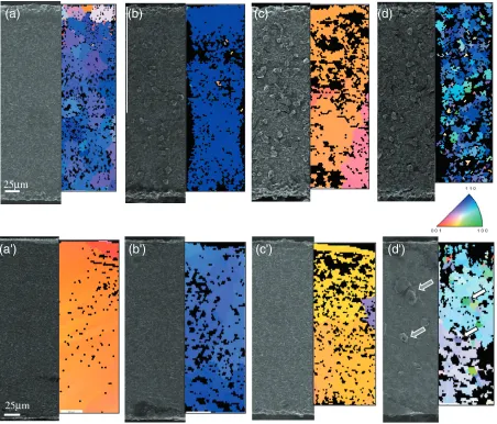
Figure 2 show a set of SEM and FIB-SIM images of the specimens with/without the reflow treatment, and before/ after the long-term thermal cycle treatment for pure-Sn and Sn-2 mass%Bi. The pure-Sn specimen without reflow treatment has equiaxed grains about 10mmin diameter, but precipitates of an intermetallic compound (IMC) such as Ni3Sn4are not recognized at grain boundaries nor inside the
grains before the thermal cycle treatment. After the thermal cycle treatment, a lot of whiskers are formed on the surface, and the Sn grains have become large as a double tens micrometer. There are few precipitates of IMC, indicating that the formation of large precipitates is limited to the region near the interface of Sn/substrate.7)For the specimen with reflow treatment, Sn grains have grown to be much large, and many precipitates of IMC are formed both at grain boundaries and inside grains. Su et al.8) also reported the EBSD result for the grain growth after a reflow treatment. After the thermal cycle treatment, there are not whiskers observed on the surface, indicating that the reflow treatment has an effect to suppress the whisker formation on pure-Sn plating. For the specimen of Sn-2 mass%Bi without reflow treatment, Sn-grains are about a few micrometers in diameter, being smaller than those in the pure-Sn specimen. After the thermal cycle treatment, the surface becomes rough but whiskers are not formed, showing a distinct
alloying-effect to suppress the whisker formation. In the specimen with reflow treatment, Sn grains have large sizes, but still small compared with those in the pure Sn specimen, and their distribution is not uniform. The number of precipitates is also smaller than that in the pure-Sn specimen. However, after the thermal cycle treatment, Sn grains have become large, associated with precipitates of IMC, and whiskers are seen to be formed on the surface. Figure 3 shows a SEM image of long whiskers of a columnar-type grown after 1500 cycles. The result shows that the reflow treatment weakens the effect of Bi-alloying to suppress the whisker formation. It is still controversial how the reflow treatment accelerates the growth of whiskers for Sn-Bi alloy plating.
In order to clarify the effect of reflow for Sn-Bi alloy plating, the variations in microstructure were observed for earlier stages of thermal cycle treatment. Figure 4 shows series of SEM images of the Sn-2 mass%Bi specimens with and without reflow treatment and before and after thermal cycle treatment of 100, 300, 500 cycles. The observed area was the central part of lead-component. It can be seen that for the specimen without reflow treatment, the surface becomes rather rough and a number of short whiskers are formed after 100 cycles, and thereafter these whiskers are developing gradually. For the specimen with the reflow treatment, on the other hand, the surface changes little until 300 cycles, but a relatively large whisker grows after 500 cycles. This result shows that the reflow treatment suppresses the formation of small nodular whiskers in the earlier stage but accelerates the formation of long columnar ones in the later stage. Figure 5 shows another series of changes in surface morphology and
10µm
10µm
(a)
(b)
(a')
(b')
(c)
(c')
(d)
(d')
Pure-Sn
Sn-2 mass%Bi
before thermal cycle treatment after thermal cycle treatment
with reflow
without reflow
with reflow
without reflow
Fig. 2 SEM images of surface morphology and FIB-SIM images after planing. Specimen; pure-Sn and Sn-2 mass%Bi. (a)(b)(c)(d) without reflow treatment, (a0)(b0)(c0)(d0) with reflow treatment of 260C. Thermal cycling treatment; (a)(a0)(c)(c0) no-treatment,
[image:2.595.124.473.71.370.2]EBSD inverse pole figure maps (normal direction) for Sn-2 mass%Bi specimens without and with the reflow treatment. The FIB-SIM image before FIB-planing and the EBSD map taken after FIB-planing are for the identical region in each specimen. It is clearly seen that the specimen without reflow treatment is made of Sn-grains around 10mmin diameter and the grains near-by have the nearly same orientations as one another to form a colony of grains. After 100 cycles, the surface becomes already rough but the grain boundaries have vanished apparently. It is thought that grain boundaries have been annealed out in part by heating in the thermal cycle treatment. However, there is a possibility that the region is
still made of small domains divided by low-angle boundaries which are not detected by the EBSD under the present condition. In the later stage of thermal cycle treatment, distinct grain boundaries are inserted to divide the grain to be small ones. After the reflow treatment, on the other hand, the Sn grains have been grown to be large, but thereafter they are divided to smaller ones gradually with the thermal cycle treatment. After 500 cycles, there are grain-colonies about 100mm in diameter that are made of small domains about 10mmin diameter.
From the experimental results shown in Fig. 2 where the grain sizes are estimated in the specimens before and after a long thermal cycle treatment, the grain size seems apparently to increase monotonously, but it is not the case. The thermal cycle treatment gives the specimens the effects of ‘‘cold-working’’ and ‘‘annealing’’ that promote ‘‘deformation’’ and ‘‘recrystallization’’, respectively. Then, the reflow treatment and/or the first heating in the thermal cycle treatment are thought to have an annealing effect to grow up the Sn-grains. In the thermal cycle treatment, the heating process has an annealing effect as well as a deformation effect due to the difference in thermal expansion coefficient between the Sn-plating and substrate, and the cooling process has a deformation effect to insert stress and dislocations. Therefore the repetitive ‘‘cold-working’’ and ‘‘annealing’’ i.e., ‘‘defor-mation’’ and ‘‘recrystallization’’ have a role of ‘‘insertion of dislocations’’ and ‘‘rearrangement of dislocations’’. There-fore, the grain size of Sn crystals increase up temporarily by the reflow-treatment and/or the first heating in the thermal cycle treatment and then decreases gradually toward a certain value by the following thermal cycle treatment. In this connection, reduction in grain size promoted by a thermal cycle treatment was reported for pure-Sn plating on a Cu substrate9)and also other metal materials.10,11)In the present case, the initial value of grain size before the reflow treatment or thermal cycle treatment is small compared with that after a long term thermal cycle treatment, leading to the result shown in Fig. 2.
Long whisker
50
µ
m
Fig. 3 SEM image of whiskers grown after 1500 cycles of the thermal cycling treatment on the specimen of Sn-2 mass%Bi with refelow treatment. The inset shows the location of test-piece observed.
(a)
(b)
(c)
(d)
10 µm
(a')
(b')
(c')
(d')
10 µm
Fig. 4 Changes in SEM images of surface morphology with thermal cycling treatment. Specimen; Sn-2 mass%Bi (a)–(d) without reflow treatment, (a0)–(d0) with reflow treatment of 260C. Thermal cycle treatment; (a)(a0) no-treatment, (b)(b0) 100 cycles, (c)(c0) 300 cycles,
[image:3.595.48.291.239.484.2] [image:3.595.73.525.545.749.2]As shown in Figs. 4 and 5, whiskers start to grow after 100 cycles on the specimen without a reflow treatment and after 500 cycles on the one with a reflow treatment. The EBSD result in Fig. 5(b) indicates that the underlying Sn layer has large grains and the whiskers have also the same orientation as the underlying layer. In the Sn layer made of small grains, on the other hand, whiskers have a different orientation from that of the domains near by in the underlying layer, as indicated in Fig. 5(d0). This suggests that the formation
mechanism could be different between the whiskers in Figs. 5(b) and (d0). The relationship in crystallographic
orientation remains as a controversial issue though. In this connection, Kimet al.12)discussed the whisker formation on Sn-10%Bi on a substrate of Cu and Fe-42%Ni with thermal cycling treatment and found that short whiskers grew more on pure Sn than on Sn-Bi.
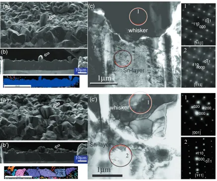
As discussed above, the thermal cycling treatment has a two-way effect of deformation and recrystallization. Then the specimen without a reflow treatment has a heterogeneous distribution in grains size, owing to a heterogeneous effect of recrystallization from location to location. Figure 6 shows the microstructures near the root of a whisker grown in the region of large grains and in the region of small ones. The whiskers
indicated with an arrow in (a) and (b), and in (a0) and (b0) are
the identical ones, respectively. EBSD maps attached are for the cross sections shown in (b) and (b0), respectively. One can
see that the surface of these specimens have the almost same morphology as each other. The EBSD maps show again that a whisker grown on a large grain has the almost same orientation as the grain, and the one on a small-grain region is located on the grain boundary and has a different orientation from either of the grains on the boundary. There are two possible explanations for Fig. 6(b), as follows: One is; a whisker grows directly from a large grain. Whiskers grown in such a way was observed in a specimen for examination of whisker growth due to external stresses,13)where the whisker growth is thought to be assisted by dislocations. The other explanation is; a whisker of a different orientation grows in the way as in the case of small grains, but thereafter the orientation becomes to be the same due to recrystallization. Unfortunately, it is not clear which is for the present. However, it is thought that the specimen without the reflow treatment contains defects and stresses in the early stage of thermal cycle treatment and they accelerate the growth of whiskers. Once a lot of whiskers start to grow, the flow of Sn atoms can be absorbed by the further growth of these
25µm
25µm
(a)
(b)
(c)
(d)
(a')
(b')
(c')
(d')
Fig. 5 Changes in FIB-SIM images of surface morphology and EBSD map with thermal cycling treatment. Specimen; Sn-2 mass%Bi; (a)–(d) without reflow treatment, (a0)–(d0) with reflow treatment of 260C. Thermal cycling treatment; (a)(a0) no-treatment, (b)(b0) 100
[image:4.595.74.526.73.459.2]whiskers. Then many whiskers are formed but most of them are short in length. On the other hand, the reflow treatment anneals out the plated specimen to retain less defects and stresses, so that there are few nuclei for whisker to grow in the early stage of thermal cycle treatment. In the later stage, the grain size become small as shown in Fig. 5(d0) and
stresses are probably accumulated to produce a chance of whisker growth. Once a few whiskers are formed, they absorb the flow of Sn atoms and grow much to be long in size as shown in (d0).
Results of TEM observation are shown in Figs. 6(c) and (c0). The electron diffraction patterns confirm the relationship
in orientation between the whisker and the grain under its root to be almost the same and quite different, respectively. The difference in brightness of TEM image between the whisker and the grain under the whisker in (c) is attributable to small differences in orientation and in foil-thickness. The region near the border between the whisker and the grain under the whisker is seen to be extremely small in foil-thickness. This morphology is attributed to an opening of grain boundaries due to formation of voids as clearly seen in (c) and preferential diffusion of Sn atoms near boundaries, a typical example of which is shown in Fig. 7. It is also found in (c) and (c0), the regions near the whisker root contain
relatively many defects such as dislocations and sub-boundaries in comparison with regions far from whiskers. This strongly suggests that defects play an important role in the growth mechanism of whiskers. The growth process and the participants of defects will be discussed elsewhere.
4. Concluding Remarks
The surface morphologies and microstructures were observed for the specimens of Sn-2 mass%Bi with and without reflow treatment after the thermal cycle treatment, and the following results were drawn.
(1) The Sn crystals in Sn-Bi specimen have small grain size compared with those in pure Sn specimen.
(2) The Sn crystals in both of Sn-Bi and pure Sn specimens without reflow treatment are smaller in size before thermal cycling treatment than those after it.
(3) The Sn crystals in Sn-Bi specimen increase their grain sizes temporarily after the reflow treatment and the heating process in the early stage of thermal cycling treatment, and then decrease the grain sizes associated with the subsequent thermal cycling treatment. The reduction in grain size reflects the competitive effects of repetitive deformation and recrys-tallization.
1
1
µ
m
2
1
2
2
1
1
1
µ
m
10µm
10µm
2
110 000
011
[111]
000011
[111] 000
200
[001] 020
110
(a)
(b)
(c)
(a')
(b')
(c')
110 000
011
[111]
whisker
whisker
Sn-layer
Sn-layer
Fig. 6 FIB-SIM images of surface and cross section and TEM image of a region near a whisker. Specimen; Sn-2 mass%Bi, without reflow treatment, after thermal cycling treatment of 100 cycles. (a)–(c) a region of a large grain (a0)–(c0) a region of small grains. (a)(a0) FIB-SIM
image of specimen surface, (b)(b0) cross sectional FIB-SIM image and EBSD-map. (c)(c0) TEM bright-field image of a region near a
[image:5.595.81.518.70.434.2](4) In the Sn-Bi specimen without reflow treatment, numerous whiskers are formed with assist of retained stress in the early stage of thermal cycling treatment, and most of them grow moderately so that they are usually small in length.
(5) The reflowed Sn-Bi specimen has a large grain size with small stress retained so that few whiskers are formed in the early stage of thermal cycling treatment. At a later stage of thermal cycling treatment, a few whiskers are formed with assist of stresses accumulated, and some of them grow to be long in size.
Acknowledgments
This work was conducted in a part of the ‘‘Sn Whisker Mitigation Project’’ supported mainly by The Organization for Small & Medium Enterprises and Regional Innovation, Japan (SMRJ), and also supported in part by The Japan Electronics and Information Technology Industries Associ-ation (JEITA) and Nanotchnology Kyushu Network of Ministry of Education, Culture, Sports and Technology, Japan (MEXT). The authors are grateful to Professor K. Suganuma and Professor Y. Ohno for their kind discussion and encouragements.
REFERENCES
1) G. T. Galyon and L. Palmer: IEEE Trans. Electro. Packag. Manuf.28
(2005) 17–30.
2) J. Smetana: IEEE Trans. Electro. Packag. Manuf.30(2007) 11–22. 3) U. Lindborg: Acta Metall.24(1976) 181–186.
4) C. Xu, Y. Zang, C. Fan and A. Abys: IEEE Trans. Electr. Packag. Manufact.28(2005) 31–35.
5) T. Kato, H. Akahoshi, M. Nakamura, T. Terasaki, T. Iwasaki, T. Hashimoto and A. Nishimura: IEEE Trans. Electro. Packag. Manuf.33
(2010) in press.
6) T. Kakeshita, K. Shimizu, R. Kawanaka and T. Hasegawa: J. Mater. Sci.17(1982) 2560–2566.
7) N. Kuwano, Jia-Yu, R. Tajima, S. Koga, S. Tsukamoto and Y. Ohno: J. Electr. Micros.53(2004) 541–544.
8) P. Su, M. Ding and S. Chopin: 2005 Electr. Comp. Tech. Conf. (2005) pp. 434–440.
9) K.-S. Kim, J.-H. Kim and S.-W. Han: Mater. Lett.62(2008) 1867– 1870.
10) Y. Nagatomo, T. Kitahara, T. Nagase, Y. Kuromitsu, H. Sosiati and N. Kuwano: Mater. Trans.49(2008) 2808–2814.
11) Y. Nagatomo, R. Muranaka, H. Hayashi, Y. Kuromitsu and N. Kuwano: Mater. Sci. Forum638/642(2010) 3895–3900.
12) N. Kuwanoet al.: unpublished data.
13) K. S. Kim, C. H. Yu and J. M. Yang: Microelectronics Reliability46
(2006) 1080–1086.
5
µ
m
(a)
(b)
[image:6.595.112.485.70.256.2]