University of Warwick institutional repository: http://go.warwick.ac.uk/wrap
A Thesis Submitted for the Degree of PhD at the University of Warwick
http://go.warwick.ac.uk/wrap/58493
This thesis is made available online and is protected by original copyright.
Please scroll down to view the document itself.
Library Declaration and Deposit Agreement
1. STUDENT DETAILS
Please complete the following:
Full name: ………. University ID number: ………
2. THESIS DEPOSIT
2.1 I understand that under my registration at the University, I am required to deposit my thesis with the University in BOTH hard copy and in digital format. The digital version should normally be saved as a single pdf file.
2.2 The hard copy will be housed in the University Library. The digital version will be deposited in the
University’s Institutional Repository (WRAP). Unless otherwise indicated (see 2.3 below) this will be made openly accessible on the Internet and will be supplied to the British Library to be made available online via its Electronic Theses Online Service (EThOS) service.
[At present, theses submitted for a Master’s degree by Research (MA, MSc, LLM, MS or MMedSci) are not being deposited in WRAP and not being made available via EthOS. This may change in future.]
2.3 In exceptional circumstances, the Chair of the Board of Graduate Studies may grant permission for an embargo to be placed on public access to the hard copy thesis for a limited period. It is also possible to apply separately for an embargo on the digital version. (Further information is available in the Guide to Examinations for Higher Degrees by Research.)
2.4 If you are depositing a thesis for a Master’s degree by Research, please complete section (a) below.
For all other research degrees, please complete both sections (a) and (b) below:
(a) Hard Copy
I hereby deposit a hard copy of my thesis in the University Library to be made publicly available to readers (please delete as appropriate) EITHER immediately OR after an embargo period of
………... months/years as agreed by the Chair of the Board of Graduate Studies. I agree that my thesis may be photocopied. YES / NO (Please delete as appropriate)
(b) Digital Copy
I hereby deposit a digital copy of my thesis to be held in WRAP and made available via EThOS.
Please choose one of the following options:
EITHER My thesis can be made publicly available online. YES / NO(Please delete as appropriate)
OR My thesis can be made publicly available only after…..[date] (Please give date)
YES / NO(Please delete as appropriate)
OR My full thesis cannot be made publicly available online but I am submitting a separately identified additional, abridged version that can be made available online.
YES / NO (Please delete as appropriate)
OR My thesis cannot be made publicly available online. YES / NO(Please delete as appropriate)
Oliver Francis John Perks
0501148
---
---
---Whether I deposit my Work personally or through an assistant or other agent, I agree to the following:
Rights granted to the University of Warwick and the British Library and the user of the thesis through this agreement are non-exclusive. I retain all rights in the thesis in its present version or future versions. I agree that the institutional repository administrators and the British Library or their agents may, without changing content, digitise and migrate the thesis to any medium or format for the purpose of future preservation and accessibility.
4. DECLARATIONS
(a) I DECLARE THAT:
I am the author and owner of the copyright in the thesis and/or I have the authority of the authors and owners of the copyright in the thesis to make this agreement. Reproduction of any part of this thesis for teaching or in academic or other forms of publication is subject to the normal limitations on the use of copyrighted materials and to the proper and full acknowledgement of its source.
The digital version of the thesis I am supplying is the same version as the final, hard-bound copy submitted in completion of my degree, once any minor corrections have been completed.
I have exercised reasonable care to ensure that the thesis is original, and does not to the best of my knowledge break any UK law or other Intellectual Property Right, or contain any confidential material.
I understand that, through the medium of the Internet, files will be available to automated agents, and may be searched and copied by, for example, text mining and plagiarism detection software.
(b) IF I HAVE AGREED (in Section 2 above) TO MAKE MY THESIS PUBLICLY AVAILABLE
DIGITALLY, I ALSO DECLARE THAT:
I grant the University of Warwick and the British Library a licence to make available on the Internet the thesis in digitised format through the Institutional Repository and through the British Library via the EThOS service.
If my thesis does include any substantial subsidiary material owned by third-party copyright holders, I have sought and obtained permission to include it in any version of my thesis available in digital format and that this permission encompasses the rights that I have granted to the University of Warwick and to the British Library.
5. LEGAL INFRINGEMENTS
I understand that neither the University of Warwick nor the British Library have any obligation to take legal action on behalf of myself, or other rights holders, in the event of infringement of intellectual property rights, breach of contract or of any other right, in the thesis.
Please sign this agreement and return it to the Graduate School Office when you submit your thesis.
U N
IV ER
SITAS WARWICEN
SIS
Addressing Parallel Application Memory
Consumption
by
Oliver Francis John Perks
A thesis submitted to The University of Warwick
in partial fulfilment of the requirements
for admission to the degree of
Doctor of Philosophy
Department of Computer Science
The University of Warwick
Recent trends in computer architecture are furthering the gap between CPU
capabilities and those of the memory system. The rise of multi-core processors
is having a dramatic effect on memory interactions, not just with respect to
performance but crucially to capacity. The slow growth of DRAM capacity,
coupled with configuration limitations, is driving up the cost of memory systems
as a proportion of total HPC platform cost.
As a result, scientific institutions are increasingly interested in application
memory consumption, and in justifying the cost associated with maintaining
high memory-per-core ratios. By studying the scaling behaviour of applications,
both in terms of runtime and memory consumption, we are able to demonstrate
a decrease in workload efficiency in low memory environments, resulting from
poor memory scalability.
Current tools are lacking in performance and analytical capabilities
motivat-ing the development of a new suite of tools for capturmotivat-ing and analysmotivat-ing memory
consumption in large scale parallel applications.
By observing and analysing memory allocations we are able to record not
only how much but more crucially where and when an application uses its
mem-ory. We use use this analysis to look at some of the key principles in application
scaling such as processor decomposition, parallelisation models and runtime
libraries, and their associated effects on memory consumption. We demonstrate
how the data storage model of OpenMPI implementations inherently prevents
scaling due to memory requirements, and investigate the benefits of different
solutions.
Finally, we show how by analysing information gathered during application
execution we can automatically generate models to predict application memory
This thesis, and the supporting research, was made possible by a great number of people. Their support throughout, both academically and personally, has maintained my focus and drive to research.
A special thank you to my supervisor Prof. Stephen Jarvis, for accepting me onto the PhD program, and supporting my research throughout.
After almost eight years at the University of Warwick, there are far too many people to thank individually, but certain people deserve special recognition. Simon Hammond, for helping me through the difficult first years of research and still being there until the end. All those with whom I work with on a daily basis: David Beckingsale, Bob Bird, Dr. Adam Chester, James Davis, Dr. Henry Franks, Dr. Matthew Leeke, Andrew Mallinson, Dr. John Pennycook and Steven Wright.
To Dr. Mark Pharaoh and Anna Wordsworth, my triathlon coaches, for keeping me sane and providing pastoral care throughout my PhD.
Andrew Herdman, Wayne Gaudin and others at AWE for providing the industry focus to my research, and general support.
Todd Gamblin for continued support of my research, and access to countless resources, both physical and intellectual.
This thesis is submitted to the University of Warwick in support of the author’s application for the degree of Doctor of Philosophy. It has been composed by the author and has not been submitted in any previous application for any degree.
The work presented (including data generated and data analysis) was carried out by the author except in the cases outlined below:
• O. F. J. Perks, S. D. Hammond, S. J. Pennycook, and S. A. Jarvis. Should We Worry About Memory Loss?, SIGMETRICS Performance Evaluation Review, March 2011 [105]
• O. F. J. Perks, S. D. Hammond, S. J. Pennycook, and S. A. Jarvis. WM-Tools - Assessing Parallel Application Memory Utilisation at Scale, In Pro-ceedings of the European Performance Engineering Workshop (EPEW), Borrowdale, UK, October 2011 [106]
• O. F. J. Perks, D. A. Beckingsale, S. D. Hammond, I. Miller, J. A.
Herdman, A. Vadgama, A. H. Bhalerao, L. He, and S. A. Jarvis. Towards Automated Memory Model Generation via Event Tracing, The Computer Journal 56(2), June 2012 [103]
• O. F. J. Perks, R. F. Bird, D. A. Beckingsale, and S. A. Jarvis. Exploit-ing Spatiotemporal Locality for Fast Call Stack Traversal, In Workshop on High-performance Infrastructure for Scalable Tools (WHIST), June 2012 [104]
The research presented in this thesis was made possible by the support of the
following benefactors and sources:
• The University of Warwick, United Kingdom:
Warwick Postgraduate Research Scholarship (2009–2013)
• Royal Society:
Industry Fellowship Scheme (IF090020/AM)
• UK Atomic Weapons Establishment:
“The Production of Predictive Models for Future Computing
Requirements” (CDK0660)
“AWE Technical Outreach Programme” (CDK0724)
API Application Programming Interface
CPU Central Processing Unit
DDR Double Data Rate
DBI Dynamic Binary Instrumentation
DIMM Dual In-line Memory Module
DRAM Dynamic Random Access Memory
ECC Error Correcting Code (Memory)
EDR Enhanced Data Rate (InfiniBand)
FDR Fourteen Data Rate (InfiniBand)
FLOP/s Floating-Point Operations per Second
HCA Host Channel Adapter (InfiniBand)
HPC High-Performance Computing
HWM High Water Mark
IB InfiniBand
ISV Independent Software Vendor
LANL Los Alamos National Laboratory
LLC Last Level Cache
LLNL Lawrence Livermore National Laboratory
MHD Magnetohydrodynamics
MPI Message Passing Interface
NUMA Non-Uniform Memory Access
QDR Quad Data Rate (InfiniBand)
RAM Random Access Memory
RDMA Remote Direct Memory Access
SDRAM Synchronous Dynamic Random Access Memory
Call Stack
The chain of function calls which brought execution to the current point.
Collective
Defines a type of communication with more than two parties involved, with
multiple sources, multiple destinations, or both. Within MPI this represents
function calls such as ‘MPI Gather’ and ‘MPI Allreduce’.
Compute Bound
A computational operation whose time is primarily decided by the time taken
to operate on the data, rather than the time to load the data into memory. In
such a scenario the use of a faster processor will afford a proportional gain in
overall performance.
Data Occupancy
The proportion of required data that is accessible in cache. High occupancy
usually equates to high efficiency computation, and relates to a compute bound
operation.
ECC RAM
Error-Correcting Code (ECC) RAM is a type of memory with built in error
detection and correction, through the use of parity bits. This makes the memory
immune to single bit errors, increasing reliability.
Ghost Cells
With parallel grid based computations it is frequently necessary to access data
which resides in another processor’s memory space. Such a situation usually
occurs at the boundary of a processor’s computational region. To improve the
performance of fetching the data, a buffer is used to replicate the whole boundary
region on the local processor. This data is rarely computed, but used as input
An application high-water-mark (HWM) is a measure of the maximum amount
of memory consumed by the application at any point during its execution. In
the case of parallel applications, we refer to HWM as being the maximum HWM
of all of the processes within the job.
Memory Bound
A computational operation whose time is primarily decided by the time taken
to load the required data into memory, rather than the actual computational
operation. In such a scenario the use of a faster processor will not afford a
gain in overall performance. Improvements in performance will only be afforded
be improvements to the memory system, such as faster RAM or more memory
bandwidth.
Paging
The process of swapping memory pages to disk, when system memory becomes
full, thus increasing memory capacity. This introduces increased access
over-heads when these pages are swapped back into memory, and is traditionally not
used in HPC configurations.
Parallel Efficiency
Is a measure of application scalability. It is defined by the parallel speedupS(p),
the parallel timeT(p) over the serial runtime T(1), divided by the number of
processors usedp.
S(p) = T(p)
T(1) (1)
E(p) = S(p)
p (2)
Point-to-Point
Defines a type of communication with a single source and destination. Within
MPI this represents ‘MPI Send’ and ‘MPI Recv’ function calls, and their
The act of increasing the core count used to solve a problem of the same size.
Weak Scaling
The act of increasing the core count used to solve a problem of increasing size,
Abstract ii
Acknowledgements iv
Declarations v
Sponsorship and Grants vii
Abbreviations viii
Definitions x
List of Figures xx
List of Tables xxii
1 Introduction 1
1.1 Motivation . . . 2
1.2 Domain . . . 3
1.3 Benchmark Applications . . . 4
1.4 Research Methodology . . . 4
1.5 Thesis Contributions . . . 5
1.6 Thesis Overview . . . 7
2 Background: Computer Memory 10 2.1 Hardware Perspective . . . 10
2.1.1 DDR Technology . . . 11
2.1.2 Trends in Memory Architecture . . . 14
2.1.3 Hardware Capacity and Costs . . . 16
2.1.6 Accelerators . . . 25
2.2 Software Perspective . . . 27
2.2.1 Allocations . . . 27
2.2.2 Virtual Memory . . . 30
2.2.3 Reporting Consumption . . . 30
2.3 Memory Reduction Techniques . . . 32
2.3.1 Memory Deduplication . . . 32
2.3.2 In Memory Compression . . . 33
2.3.3 AMR . . . 33
2.4 Summary . . . 34
3 Background: Memory Analysis Tools 35 3.1 Types of Tool . . . 35
3.1.1 Debugging . . . 35
3.1.2 Profiling . . . 36
3.2 Interface Methodology . . . 37
3.2.1 API . . . 37
3.2.2 Interposition . . . 38
3.2.3 Code Injection / Pre-processing . . . 38
3.2.4 DBI . . . 39
3.2.5 Sampling . . . 40
3.2.6 Lightweight and Heavyweight Tools . . . 41
3.3 Related Tools . . . 41
3.3.1 memP . . . 42
3.3.2 MAP . . . 42
3.3.3 MEMWATCH . . . 43
3.3.4 Valgrind . . . 43
3.3.5 Existing Tool Critique . . . 44
4 WMTools 47
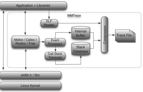
4.1 WMTrace - Data Collection . . . 47
4.1.1 Library Structure . . . 48
4.1.2 Application Interaction . . . 49
4.1.3 Data Storage . . . 50
4.2 WMAnalysis - Data Analysis . . . 51
4.2.1 Analysis Phase . . . 52
4.2.2 HWM Analysis . . . 52
4.2.3 Functional Breakdown . . . 55
4.2.4 Temporal Graph . . . 56
4.2.5 Temporal Function Graphs . . . 58
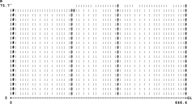
4.2.6 Heat Map . . . 59
4.2.7 Comparative Analytics . . . 61
4.3 Comparison . . . 63
4.3.1 Functionality . . . 63
4.3.2 Performance . . . 68
4.4 Project Availability . . . 70
4.5 Summary . . . 70
5 Workload Analysis and Memory Scalability 72 5.1 Related Work . . . 73
5.2 Application Memory Consumption . . . 74
5.3 Simulating Effects of System Memory Loss . . . 76
5.3.1 Workload Construction . . . 76
5.3.2 Machine Simulation . . . 77
5.3.3 Performance Analysis . . . 78
5.4 Understanding Scalability . . . 80
5.4.1 Ghost Cells . . . 81
5.4.4 Communication Buffers . . . 88
5.5 Summary . . . 88
6 MPI Memory Consumption 90 6.1 InfiniBand Communication . . . 91
6.1.1 MPI Receive Queues . . . 92
6.1.2 InfiniBand Interface . . . 92
6.2 Related Work . . . 93
6.3 Application Profile . . . 95
6.3.1 Application Communication Classification . . . 96
6.3.2 Application Memory Profile . . . 98
6.4 Identifying MPI Memory Consumption . . . 99
6.5 MPI Implementation Comparison . . . 102
6.6 Runtime Configurations . . . 102
6.7 Vendor Libraries . . . 105
6.7.1 MXM . . . 105
6.7.2 PSM . . . 106
6.8 Application Modifications . . . 107
6.9 Summary . . . 108
7 Memory Modelling 110 7.1 Related Work . . . 111
7.2 Point-wise Comparison . . . 113
7.2.1 Linear Regression . . . 114
7.2.2 Misinterpretation of Relationships . . . 114
7.3 Lare2D - Simplistic Model . . . 115
7.3.1 Multiple Models . . . 118
7.3.2 Increased Problem Size . . . 118
7.4 Chimaera - Complex Model . . . 119
7.5.1 3D Processor Decomposition . . . 124
7.5.2 Hybrid MPI and OpenMP . . . 125
7.6 Model Confidence . . . 128
7.7 Summary . . . 128
8 Conclusion 130 8.1 Contributions . . . 131
8.1.1 Beneficiaries . . . 133
8.2 Limitations . . . 133
8.2.1 Data Volume . . . 134
8.2.2 Technologies . . . 134
8.3 Future Work . . . 136
8.3.1 Static Source Code Analysis . . . 136
8.3.2 Mixed Mode Data Collection . . . 137
8.3.3 Model Prediction Validations . . . 138
8.3.4 Power Consumption . . . 138
Bibliography 139 Appendices 153 A Context: Architectures and Applications 154 A.1 Machines . . . 154
A.1.1 Cab (LLNL) . . . 155
A.1.2 Hera (LLNL) . . . 156
A.1.3 Minerva (Warwick) . . . 157
A.1.4 Kay (Bull) . . . 158
A.2 Applications . . . 159
A.2.1 Chimaera (AWE) . . . 159
A.2.2 Orthrus (AWE) . . . 160
A.2.5 Sweep3D (LANL) . . . 160
A.2.6 NPB (NASA) . . . 161
A.2.7 LAMMPS (SNL) . . . 161
A.2.8 MiniFE (SNL) . . . 161
A.2.9 phdMesh (SNL) . . . 162
A.2.10 Lare2D (Warwick) . . . 162
2.1 Hierarchal overview of traditional memory subsystem . . . 11
2.2 LLC size of processors over time . . . 15
2.3 Top 5 supercomputer memory per core ratios . . . 16
2.4 DRAM cost capacity comparison . . . 19
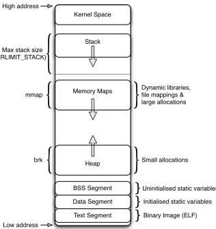
2.5 Structure of virtual memory address space for application . . . . 29
4.1 WMTrace data collection process . . . 48
4.2 Per rank HWM distribution for Chimera 1203on 128 cores . . . 54
4.3 Comparison of maximum and minimum HWM threads for
Chi-maera 1203on 128 cores . . . . 57
4.4 Rank 48 temporal functional graph for Chimera 1203on 128 cores 59
4.5 Heat Map at point of HWM for Chimera 1203on 128 cores . . . 60
4.6 WMTrace analysis of Chimaera on 64 cores . . . 64
4.7 MAP analysis of Chimaera on 64 cores . . . 65
4.8 Valgrind Massif temporal graph for Chimera 1203on 64 cores . . 67
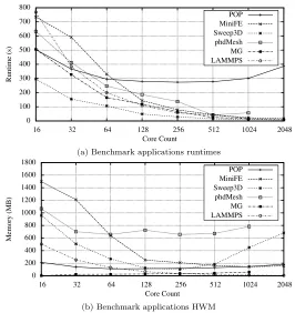
5.1 Runtime and HWM scaling behaviour for benchmark applications
on Hera . . . 75
5.2 Simulated runtimes for workloads with different memory
restric-tions . . . 79
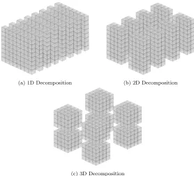
5.3 Data dependency and ghost cells in a cube . . . 81
5.4 Decompositions of an 83cube onto eight processes . . . . 82
5.5 Proportion of ghost cells as a percentage of total cells in different
decompositions of a 10243cube . . . . 83
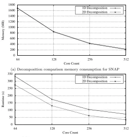
5.6 1D and 2D decomposition comparison for SNAP . . . 85
128 cores . . . 98
6.2 Frequency distribution of message sizes on 128 cores . . . 99
6.3 Temporal memory usage for Orthrus on128 cores . . . 99
6.4 Orthrus MPI memory consumption at 1024 cores . . . 100
6.5 Platform comparison of Orthrus memory scalability with OpenMPI101
6.6 Orthrus BullXMPI comparison with low memory profile on Kay
- Mellanox . . . 104
6.7 Orthrus using MXM comparison with default OpenMPI on Kay
- Mellanox . . . 106
6.8 Orthrus using PSM comparison with default OpenMPI on Cab
-QLogic . . . 107
7.1 Model prediction against temporal trace of Lare2D on 16 cores . 117
7.2 Model prediction against temporal trace of Lare2D on 128 cores . 117
7.3 Chimaera MPI memory growth against model prediction . . . 122
A.1 Node level structure of Cab . . . 155
A.2 Node level structure of Hera . . . 156
A.3 Node level structure of Minerva . . . 157
4.1 Chimaera HWM strong scaling profiles . . . 53
(a) 603HWM profile . . . . 53
(b) 1203HWM profile . . . . 53
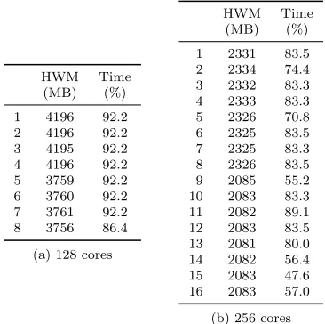
4.2 Chimaera node level HWM for 1203 . . . . 62
(a) 128 cores . . . 62
(b) 256 cores . . . 62
4.3 Memory tool feature comparison . . . 63
4.4 Memory tool overhead comparison for Chimaera 1203on 64 cores 68
5.1 Mixed application workload compositions . . . 76
5.2 Percentage runtime increase from 1536 MB to 682 MB per core . 78
6.1 Different communications at 64, 128 and 256 cores . . . 97
7.1 High water mark results forLare2D40962 . . . 115
7.2 Model prediction results forLare2D40962 . . . 116
7.3 Second model prediction results forLare2D40962. . . 118
7.4 Compound model prediction results forLare2D81922 . . . 119
7.5 Model validation for Chimaera . . . 121
(a) Chimaera 1203 . . . 121
(b) Chimaera 603 . . . 121
7.6 Model predictions for Chimaera using Equation 7.5 . . . 123
7.7 Model predictions for Chimaera with 3D processor decomposition 124
(a) Chimaera 603 . . . 124
(b) Chimaera 1203 . . . 124
7.8 Model predictions for Chimaera with hybrid parallelism . . . 126
Introduction
High performance computing (HPC) has become the cornerstone of many
scien-tific disciplines, supporting experimentation through simulation to reduce cost
and mitigate risk.
Whilst the benefits of HPC have been apparent to large scientific institutions
for many decades, such systems have traditionally been prohibitively expensive
for smaller companies and research groups. The rise of commodity computing
has since lowered the machine cost and released the potential of HPC in many
new domains.
Recent developments in parallel processing hardware, such as multi-core
commodity processors, have had a dramatic effect on the performance of these
supercomputing platforms. The evolving technologies constantly striving for
increased performance at the high end of supercomputing result in a ‘trickling
down’ of technologies, and their associated performance, to commodity
com-puting. From historical analysis we can see that it only takes between six and
eight years for the slowest machine in the Top500 list [82] to achieve the same
computational power of the number one machine. Beyond the HPC domain we
see that it only takes eight to ten years for a notebook computer to replicate
the performance of that slowest machine in the Top500 [83].
Whilst the majority of media, and industry, attention has traditionally
focused on the computational power of CPU architectures, the increased scale
of modern HPC platforms has identified a number of other performance
bot-tlenecks. Most scientific applications can be classified by their dependence
on the four key components of computing: computational power; memory
veritable neglect of these other components has stifled performance gains for
many large scale scientific applications. To address this architectural imbalance
the proportional component cost of supercomputers has been slowly evolving,
and as such memory is consuming a larger portion of machine procurement
budget than ever before.
In this thesis we focus on the role of computer memory in the HPC ecosystem,
specifically focusing on memory capacity and utilisation. Whilst not directly a
performance modifier, memory consumption and associated scaling will have
a dramatic effect on available runtime configurations, dictating core counts
and problem sizes. We also address how, in many situations, there is an
inherent tradeoff between performance and memory usage, motivating the use
of non-optimal techniques to reduce memory footprints and thereby enable the
execution of larger problems.
1.1
Motivation
The rise of multi-core processors, and their increasing core count densities, is
having a dramatic effect on memory-per-core ratios. The rate of technological
development in computer memory (DRAM) has not matched equivalent
ad-vances in CPU architecture. Specifically, the rate of growth of DRAM capacity
has not been proportional to the increase in CPU core counts. Where high
capacity DRAM modules are available they are often prohibitively expensive,
or their usage comes with performance limiting caveats.
Within HPC a job’s memory is provisioned on a per-core or per-node basis,
defining constraints based on physical resources and resource sharing policies.
Failure to adhere to these restrictions results in job termination, often
with-out warning or accurate error reporting, thus job configuration and accurate
resource provisioning are crucial for maintaining a productive computational
environment.
an algorithmic expectation of usage and experimental experience of failing jobs.
Historically it has often been cost effective to over-provision memory resources
to prevent job failures, but with rising costs this option is becoming harder and
harder to justify. As such it is increasingly important to accurately provision
memory capacity resources during machine procurement, where the balance
between cost and usability is most critical.
The rising scale of the jobs mean that it is harder to algorithmically predict
memory usage, as other factors begin to play a more crucial role in memory
consumption, and the failure of jobs is less acceptable as they waste valuable
machine time. For this reason it is now key to fully understand the memory
usage characteristics of key scientific applications in HPC institutions. Code
users and system designers are increasingly looking towards software tools to
provide and analyse this information.
Where application memory requirements are prohibitively disproportionate
to others in an institution’s workload, code engineers must look to reduce
their memory consumption. This reduction can come in two different forms;
either more memory efficient runtime configurations or the re-engineering of
applications libraries. Again scientists look to tools to provide analytical insight
into the cause of consumption, and validation of the results of any memory
reduction exercise.
As such the tool chain supporting memory consumption analysis must be
strong enough to support high level application analysis as well as fine gained
analysis. We do not feel that these requirements are accurately provisioned for
by existing memory analysis tools, and therefore propose the development of a
new suite of tools to provide this level of data analysis.
1.2
Domain
Within this thesis we are concerned with the memory capacity, and associated
many of the topics we discuss have a broader scope, we limit ourselves to focusing
on the application of such topics to supercomputers. In the case of our
discus-sions on computer hardware we touch upon only a subset of technologies, to
facilitate a more in-depth evaluation of HPC-centric hardware. Whilst elements
of other hardware technologies may be applicable we try to maintain focus on
current, and anticipated, industry trends.
Similarly the tools and methodology we present are not necessarily confined
to HPC applications and architectures but we deliberately constrain ourselves
to the field to demonstrate their capabilities.
1.3
Benchmark Applications
Throughout this thesis we make use of a wide range of benchmark applications.
Each of these applications is used specifically to demonstrate the capabilities of
different memory consumption analysis techniques. The choice of each
applica-tion is designed to expose certain memory behavioural characteristics which are
best investigated with the current technique. Although most of the techniques
could be applied to all of the applications discussed, we do not believe that an
interesting insight could be gained with every combination.
A full description of the applications used is presented in Appendix A.2.
1.4
Research Methodology
In this thesis we ask – to what extent can non-intrusive profiling methods be
used to analyse application memory consumption? We look to provide code
developers with the tools and methodologies to evaluate the precise reason for
behavioural characteristics in memory consumption, with the ultimate goal of
re-ducing application memory high water mark. Memory is an increasingly crucial
component of parallel applications, with financial and physical constraints
parallelism is achieved, and how resources can be best utilised. Existing tools
are very limited in their capabilities to deliver fine-grained analysis into how
and where application memory consumption especially in relation to job scale.
In this research we explore the capabilities of memory consumption analysis
for increasing the scalability of applications, and in the process future-proofing
them against trends in declining memory-per-core ratios.
To answer this question we employ quantitive methodologies. Through
empirical analysis of parallel application we study relationships in memory
consumption.
The early portion of this research is dedicated to the development of tools,
of sufficient quality, to provide observational information regarding application
memory behaviour. The latter is dedicated to the analysis of this information
and the construction of hypotheses. Where possible we verify these hypotheses
and evaluate their impact through more empirical testing.
1.5
Thesis Contributions
This thesis is based around the development of a memory consumption analysis
tool, and its application in understanding different aspects of the memory
utilisation of HPC applications.
Our analysis serves two purposes: the first is the understanding of an
appli-cation’s memory profile with sufficient detail to accurately provision hardware
resources, either during job submission or machine procurement; the second is
providing a much deeper level of understanding to facilitate code re-engineering
to reduce memory consumption.
In addition to the presentation of our tools and methodologies we present
three investigations into application behaviour, driven by a need to understand
memory consumption behaviour.
mem-resulting data. We develop a suite of tools to achieve this data collection,
and the associated analysis, to demonstrate the validity and capability of the
methodology. For each method of analysis we present an example of where the
tools can be used to improve understanding of the underlying application.
Scaling Analysis We show how memory consumption analysis can be applied
to a full machine workload. We show how strong scaling can be used to facilitate
the deployment of low memory machines, and analyse the viability of such
platforms through efficiency analysis on simulated workloads. To further the
potential of this method, we address some of the concepts and techniques
for reducing ghost cells to improve memory consumption scalability without
detriment to performance.
MPI Memory Analysis We apply our analysis to evaluate the impact of
MPI implementation choice, for specific network hardware. By looking at the
memory consumption attributed to MPI on different platforms, for different
implementations, we identify the best configurations to improve memory
con-sumption scalability.
Automated Memory Modelling We investigate the potential of using
mem-ory consumption traces to automatically generate predictive models for memmem-ory
high water mark. Using allocation size comparisons we can predict memory
con-sumption at different scales, both in terms of problem size and core count, with
a high degree of accuracy based on data from only two runs. We further show
how these models can be used to predict the memory effects of implementing
new programming principles, such as 3D processor decompositions and hybrid
MPI and OpenMP parallelism.
These contributions show how far non-intrusive methods of memory
consump-tion profiling can be extended to provide critical analysis for applicaconsump-tion
consumption, and critically monitor the artefacts of consumption as the size of
the job is scaled. The fine-grained analysis allows us to study potential issues at
small scale before they become dominant problems at large scale. Additionally
we show how this data can be used for predicting memory consumption at scales
greater than those obtainable with current configurations.
1.6
Thesis Overview
The remainder of this thesis is organised in the following way:
Chapter 2 presents an introduction to computer memory, divided into two
logical sections to discuss memory in terms of both hardware and software. We
discuss why architectural nuances influence trends, and help determine memory
capacity, coupled with an analysis of core counts to understand memory-per-core
ratios. Additionally we discuss how memory is used within the system, and use
this to understand differences in the way memory usage is reported to the user.
In Chapter 3 we continue with our introduction, but within the domain of
software tools, presenting some key concepts and methodologies. We discuss
the fundamental differences between tool types, and the roles that they play in
the software ecosystem. Further more we discuss the methods of data
collec-tion utilised by these tools and evaluate their inherent performance properties.
Within the domain of memory analysis, we present a discussion of a number
of different software tools, evaluating them on the data they can collect and
analysis they can perform. We use this evaluation to motivate the development
of a new memory analysis tool, by identifying their limitations and desired
functionality.
Chapter 4 presents the development of our memory analysis tool suite,
WMTools, and features a demonstration of the various analysis methods applied
to the AWE Chimaera benchmark application. We detail the key design
prin-ciples, based on our previous evaluation of existing tools, and describe how our
analysis.
In Chapter 5 we investigate the memory scalability of applications,
us-ing strong scalus-ing to reduce memory-per-core footprints. We use HWM data,
with accompanying runtime data, to simulate the execution of mixed science
workloads on computers with decreasing memory-per-core ratios. From this
we are able to show the decrease in workload efficiency resulting from such
usage, caused by the poor memory scalability of some applications. We further
investigate the cause of poor memory scalability by demonstrating the impact
of ghost cells, and present a number of memory reduction techniques such as
processor decompositions and hybrid parallelism programming models.
Chapter 6 presents an investigation into MPI memory consumption, and
the associated impact of communication buffers when strong scaling
applica-tions. Through analysis of a benchmark application we evaluate the memory
scalability of different MPI implementations and different InfiniBand hardware.
We experiment with a range of improved implementations to show how MPI
memory consumption, which can grow at an alarmingly rate, can be reduced to
more manageable levels.
In Chapter 7 we demonstrate the ability to generate automated memory
models based on the execution traces from WMTools. We look at two cases: a
simplistic model of Lare2D, where we construct two different models to capture
the characteristics of two code regions; and the more complex modelling of
Chimaera, where we capture the artefacts of ghost cells. We validate these
models against results from strong scaling and a change in problem size. We
then use the Chimaera model to generate predictions for memory savings based
on 3D processor decompositions, and hybrid programming model, in accordance
to the effects demonstrated in the latter half of Chapter 5.
In Chapter 8 we conclude this body of research by reiterating the
contri-butions, discussing limitations to the research and detailing future work in the
same domain.
Background: Computer Memory
In this chapter we present an overview of the memory subsystem within modern
computers, with respect to both hardware and software. We describe the
different layers in the memory hierarchy and where our research interests sit.
Additionally we look at current hardware trends, and from this identify a
number of issues with current memory hardware. From this we discuss a number
of future and emerging technologies, and describe the ways in which they address
current problems in hardware.
From a software perspective we discuss the structure of applications in
virtual memory, and how this relates to application memory consumption.
We discuss different methodologies for measuring memory consumption and
their limitations, and use this discussion to motivate our choice of measuring
application level memory management in memory studies, both for accuracy
and information availability.
2.1
Hardware Perspective
Figure 2.1 outlines the different layers of the memory subsystem hierarchy. The
closer a layer is to the top of the pyramid, the closer it is to the logic units of the
processor, and also the faster it is. The limitation of proximity is size, meaning
to be close and fast the memory layer must also be small, thus the largest layers
sit furthest away from the processor’s logic units.
The majority of memory allocations are handled by the Random Access
Memory (RAM), a layer built on the inherent tradeoff between capacity and
performance. When the specific pages of memory are required by the application
CPU Registers
L1 Cache L2 Cache L3 Cache (Optional)
Random Access Memory
Hard Disk Drive
Performance Capacity
[image:36.612.228.385.118.241.2]On CPU Chip
Figure 2.1: Hierarchal overview of traditional memory subsystem
In this thesis we are solely concerned with RAM, and the issues surrounding
capacity limitations. The performance of RAM is already considered a
bottle-neck in memory bound applications, thus having to resort to another layer of
the hierarchy to achieve sufficient capacity is not considered a viable option [34].
Within the HPC community the use of Error Correcting Code (ECC) RAM
is standard, as a measure to reduce errors in calculations, thus increasing the
accuracy of scientific applications and increasing overall system stability [42].
One of the downsides to ECC RAM is the increased cost, with chips often
costing twice as much as equivalent non-ECC RAM. This is, partly, a result of
requiring an additional storage for the parity bit, but mainly to do with the
limited market as ECC RAM is not common in desktop computers.
Software level ECC, such as that provided in many Graphics Processing
Units (GPUs), result in a capacity reduction of 12.5% with an associated
reduc-tion in memory bandwidth.
2.1.1
DDR Technology
Main computer memory is traditionally comprised of Double Data Rate (DDR)
memory Dual In-line Memory Modules (DIMMs) composed of SDRAM memory
modules. The current generation of DDR is DDR3, which provides a doubling
of data rate at a reduced voltage over the previous DDR2 generation. The next
architectures such as Intel’s Haswell-E processors, with increased clock speeds
at a further reduced voltage.
There are a number of competing DIMM technologies currently used within
DDR3, each with a different emphasis on a different aspect of technology.
Whilst these other technologies are available, RDIMM remains the most
com-mon DRAM used in HPC platforms due to the trade-off between cost, capacity
and performance.
Ranks
DDR DIMMs are often referred to in terms of ranks: single, dual, quad and
the emerging octal rank. The rank describes the number of modules, group of
similar DRAM chips, on a DIMM. Each rank has a maximum capacity based
on DRAM chip capacity and payload.
For example a quad rank RDIMM can support up to 32 GB, with a rank
width of 72 bits for ECC support, by utilising 16 × 4 Gb DRAM chips each
rank can support up to 8 GB [52].
Thus to achieve higher DIMM capacity one must either increase the number
of ranks, or the the rank capacity. The introduction of 8 Gb DRAM technology
will facilitate the development of 64 GB RDIMMs, alternatively moving to octal
rank LRDIMMs which can support up to 64 GB [84].
RDIMM
Registered DIMMs contain a register to buffer the address and control lines in
addition to the clock. This makes a more stable memory system, allowing for
higher capacity DIMMs and, often, the use of more DIMMs per channel. This
buffering does introduce a minor latency, and can reduce bandwidth when using
a single DIMM per memory channel. The additional hardware and relatively
UDIMM
Unregistered DIMMs are slightly cheaper than comparable RDIMMs, at smaller
capacities (2 GB to 4 GB). Each UDIMM installed introduces electrical load
and issues with noise [63]. Achieving higher capacities without buffering is
harder, meaning there is limited availability of the highest capacity DIMMs
(8 GB), and they are often more expensive than RDIMMs. Within HPC the
use of UDIMMs is not popular, due to the unattractive price-per-GB and the
restrictions on configurations.
FBDIMM
Whilst FBDIMMs are no longer favoured, their technological achievements make
them an interesting point of discussion. Fully Buffered DIMMs were designed
to increase the number of DIMM slots supported on each memory channel, by
providing an area of on-chip memory to act as an advanced memory buffer
(AMB) [43]. Through the use of a serial bus the memory channel would
communicate with the AMB providing some error correction and facilitating
the issuing of parallel read/write commands, as they can be buffered.
In addition to increased cost FBDIMMs were plagued with power usage
and heat dissipation issues [74], and were not widely adopted. Many
manu-facturers have since ceased production, and removed the technology from their
roadmap. The technological benefits behind FBDIMMs are very desirable and
work to replicate them is still underway; we discuss some of these projects in
Section 2.1.5.
LRDIMM and HCDIMM
Load Reduced DIMMs and Hyper Cloud DIMMs are very similar in concept,
as an amalgamation of RDIMM and FBDIMM technology. In addition to the
buffering done by RDIMMs they buffer the data lines, making all lines fully
buffered. The reduction in electrical loading on the chips, due to the buffer
Quad rank LRDIMMs utilise their rank multiplication to present their four
logical ranks as two virtual ranks, enabling three quad rank chips to appear
as six virtual ranks. The increase in rank capability enables the use of higher
capacity DIMMs.
HCDIMM differs from LRDIMM by providing logic support without the need
for BIOS configuration. This is claimed to provide an increase in bandwidth
and throughput [95].
The cost of LRDIMM, and HCDIMM, is slightly more than RDIMM due to
the additional logic and limited market prevalence.
DDR Data Rate
DDR stands for double data rate. This is the process of ‘double-pumping’ data
with regards to the clock – data is transferred on both the rise and the fall of
the clock signal. This results in a slight confusion of terms, generally amongst
vendors, between clock rate Megahertz (MHz) and data rate Mega-Transfers per
second (MT/s). A chip labeled DDR3-1600 will have a data rate of 1600 MT/s,
resulting from a clock speed of half that figure, 800 MHz, though many vendors,
and other sources, may incorrectly label it as 1600 MHz.
During this thesis we refer exclusively to the data transfer rate to avoid
confusion.
2.1.2
Trends in Memory Architecture
In this section we will look at some of the underlying trends in hardware
technology and machine architecture. Using the ‘CPU DB’ data set from the
Stanford VSLI group [28] we are able to track architectural changes in a number
of key regions for a wide range of processors from the past 40 years. We note
that whilst this data set is significant it does lack details of a number of more
recent architectures. Additionally we compile data from the Top 500 list of
supercomputers [82] looking at the historical trends of the largest
64 128 256 512 1024 2048 4096 8192 16384 32768
1994 1996 1998 2000 2002 2004 2006 2008 2010 2012
LLC
Size
(KB)
Release Date 1 Core
2 Core 3 Core 4 Core 6 Core 8 Core
Figure 2.2: LLC size of processors over time
specification database. Specifically we use information collected about the server
grade products: the E7, E5, E3, 7000, 6000, 5000 and 3000 product lines.
Kogge and Dysart presented a more comprehensive analysis of the Top
500 list, evaluating historical trends and making future projections based on
roadmaps [65]. From this study they are able to observe the fall in the bytes
/ FLOP metric, a comparative measure of storage to compute capacity. They
attribute this, in part, to the rise of lightweight and heterogeneous systems.
Cache Size
Figure 2.2 plots the size of the Last Level Cache (LLC) (either L2 or L3
depending on the architecture) against the processor’s release date. Additionally
we have grouped the data by the number of cores on the processor, which allows
us to view the different trends in architecture design. We can clearly see that
over time the LLC size is increasing, signifying its importance in modern day
computing. There is also no discernible trend between core count and cache size;
a number of single and dual core chips have equivalent cache sizes as chips with
higher core counts. Some patterns are clearly visible though, like the preference
for 2 MB per core, resulting in a number of quad core chips with 8 MB of LLC
0 1 2 3 4 5 6
07-2008 01-2009 07-2009 01-2010 07-2010 01-2011 07-2011 01-2012 07-2012 01-2013
Memory
/
Core
(GB)
List Date Top 5 Average
Figure 2.3: Top 5 supercomputer memory per core ratios
Memory Per Core
Using the Top500 list we collect information on the top five systems from each
list, and plot their memory per core ratios. For heterogeneous systems we
represent only the ratio of DRAM to CPU cores, and exclude GPU processing
and memory capacity.
Figure 2.3 shows this trend over the last five years. What we see from this
graph is that the average memory per core of the top five systems is actually
quite constant, generally between 1.5 GB and 2.5 GB per core.
Whist we do not observe a decline in memory-per-core ratios, as expected,
we attribute this to the extreme scale of the platforms analysed. At the top
end of HPC price is always a dominating factor and so memory capacity has
always been constrained. Although we do not have sufficient data to analyse the
full 500 machines in the list, we would expect to observe some capacity-based
trends. Whilst we observed in Chapter 1 that it only takes six to eight years for
the performance of the top computers to be amortised into the lower echelons to
the Top 500 list, we do not believe this trend to hold true for memory-per-core
ratios.
2.1.3
Hardware Capacity and Costs
The memory capacity of computers is controlled by two factors: physical
architecture influences memory capacity, through configuration options, and
briefly investigate the financial considerations.
From this we show that the challenges to maintain existing memory-per-core
ratios is managing the DIMM configurations to minimise financial overheads. In
other, more memory constrained, domains the limitations on memory capacity
are resulting in the proposal of novel architectures such as disaggregated memory
systems [73].
Memory Channels
Current generations of Intel processors support up to four memory channels
per processor [55], which determines bandwidth. Each memory channel can
normally support three DIMMs [88, 89] of up to 32 GB in capacity. This gives a
theoretical maximum capacity of 768 GB for a two socket, four memory channel,
three DIMMs-per-channel (DPC) 32 GB DIMMs configuration, though such a
configuration is highly expensive.
Intel does support up to four DPC through the use of the Intel 7500
genera-tion chipset, which supports Scalable Memory Buffer (SMB) [56, 57]. Building
on the principles of FBDIMMs, the SMB acts as an intermediary operation
buffer, but utilises traditional DDR3 RDIMMs. Each SMB provides two
mem-ory channels, each supporting eight logical ranks, allowing the use of four quad
rank chips per SMB.
The 7500 chipsets are generally used for very memory dense servers,
theoret-ically allowing up to 4096 GB, when the 128 DIMM slots of an 8-socket server
are populated with 32 GB DIMMs.
With regards to memory systems, Intel and AMD based architectures are
very similar, and so assertions illustrated with Intel based examples are also
gen-erally applicable to AMD as well. The AMD ‘Magny Cours’ micro-architecture
exhibits many of the same memory subsystem configurations as Intel’s
‘Ne-halem’ micro-architecture including an integrated memory controller [23]. Both
three DPC.
The AMD ‘Interlagos’ architecture is slightly different as each CPU is made
up of two logical dies, with each die containing up to four ‘Bulldozer’ modules
(two ‘cores’ with a shared floating point unit). Each die has its own memory
controller with two memory channels, giving a total of four channels per CPU.
The IBM Power architecture is similar to the Interlargos architecture in the
way that multiple dies, with independent memory controllers, are contained
within the same chip [53].
The future Haswell-E architecture from Intel, which will support DDR4, is
rumoured to contain only four memory channels, similar to current generations,
and be limited to one DPC due to the use of octal rank DIMMs.
Hardware Limitations
Although the memory capacities discussed above are theoretically achievable,
in practice it is not always that easy. Whilst the use of three DPC is supported
configuring such a system is non trivial [11, 41, 120]. UDIMMs only support a
maximum of two DPC, with a maximum combined capacity of 64 GB.
Memory channels can support a maximum of eight logical ranks each, this
means up to two quad rank DIMMs or a mixture of three dual or single rank
DIMMs. 32 GB RDIMMs are only available in quad rank, which is only
supported in two DPC mode, thus limiting the maximum memory capacity
to 64 GB per channel.
LRDIMMs can be run in three DPC mode with ‘quad rank’ chips, as they
will appear as a combined six virtual ranks, enabling up to 96 GB per memory
channel. One limitation is that such a configuration can only be supported
in reduced performance mode, reducing the I/O clock speed from 666 MHz
to 533 MHZ, resulting in a reduction of transfer rate from 1333 MT/s to
1066 MT/s.
Additionally some system configurations will not allow the use of low voltage
0 200 400 600 800 1000
2 4 8 16 32
0 10 20 30 40 50
DIMM
Costs
($)
Mean
Cost
/
GB
($)
DIMM Capacity (GB) DIMM Costs
Mean Cost/GB
Figure 2.4: DRAM cost capacity comparison
the increased noise and signal degradation.
DIMM Cost
To maintain established memory-per-core ratios, within nodes with increased
core counts, nodes must increase their memory capacity accordingly. Often it
is not just the case of adding more memory DIMMs to the specific nodes.
In Figure 2.4 we present an evaluation on the current list price of DDR3
RDIMM chips with ECC support from Crucial as of June 2013 [25]. We
present the cost-per-DIMM of varying DIMM capacities, factoring in the cost
of different speeds and configurations, in addition to the average cost-per-GB
of each capacity DIMM. What we see from this figure is that whilst initially
the cost-per-GB decreases, to a ‘sweet spot’ at 8 GB DIMMs, the cost-per-GB
then starts increasing, demonstrating that higher capacity DIMMs are less cost
effective.
In a DIMM count-constrained environment the system architect will have to
utilise higher capacity DIMMs to maintain memory-per-core ratios in high core
count configurations. The implication of this figure is that such a configuration
is less efficient in terms of cost-per-GB, thus driving up the total cost of the
machine.
con-sumers, at small purchasing scale, we believe the trend to be representative
of larger procurements. A discussion on relative DIMM costs by Fujitsu also
concluded a price-per-GB sweet spot at 8 GB DIMMS [41]. They also
high-light how UDIMM is comparatively cheaper than RDIMM, and LRDIMM is
comparatively more expensive, supporting our descriptions in Section 2.1.1.
Power Consumption
Whilst the power consumption of individual DDR3 DIMMs is considered to be
fairly low, the cost is multiplied by their sheer multitude. There are two factors
to take into account with DIMM power consumption: idle power and active
power.
HP report the active power consumption of an 8 GB dual rank low-voltage
(1.35 V) RDIMM to range from between 3.5 to 5 W, depending on speed [50].
This falls to about 0.5 W when idle, regardless of speed.
If we take for example a cluster, similar in configuration to Bull’s Kay
platform, of a 1000 dual socket nodes utilising oct-core Intel E5-2580s, with
a maximum Thermal Design Power (TDP) of 130 W and 8 GB low-voltage
RDIMMs. Maintaining a memory-per-core ratio of 4 GB will consume in the
region of 40 kW when actively used, compared to the ≈20 kW required to
maintain an active 2 GB-per-core ratio. This is in contrast to the theoretical
maximum of 260 kW consumed by the processors in such a system, but still
represents a significant power consumption saving.
These figures also motivate our research into memory consumption
reduc-tion, as the potential power savings from reducing memory use are significant.
2.1.4
Challenges in Memory Technology
There are three challenges with current memory technology that need addressing
in the future: capacity, performance (latency and bandwidth) and power. The
technological requirements of these problems can be largely distinct, for example
progression in all three domains is required.
The Memory Wall
The original concept of ‘The Memory Wall’ addressed the issue of the
perfor-mance gap between processors and memory with respect to latency [128]. The
concept states that the discrepancy between the rate of improvement between
processor performance and memory latency would eventually lead to a state
where every operation is memory bound, that processing would be so quick
that the defining limiter on computation time would be the memory fetches for
each piece of data that needed computing.
Technological developments have drawn out the effects of ‘the wall’ but it is
still anticipated to influence future platforms.
Rise of Many-core
One of the biggest changes in the performance landscape, from a memory
perspective, is the rise of many-core. Multi-socket systems often utilise separate
NUMA regions, enabling a duplication of memory subsystems. Many-core, on
the other hand, increases core count but using the same fundamental memory
subsystem.
The additional resource contention, resulting from more cores utilising a
similar number of memory channels, has lead to a stark performance gap. The
increase in processor cores has not been met with an equivalent quantity of
increases in other regions of the memory subsystem [79].
One of the implications, of particular interest to this body of research, is the
impact on memory-per-core ratios. Whilst DIMM capacity is increasing, albeit
slowly, the only way of maintaining memory-per-core ratios is to increase DIMM
count. This has implications for both power and performance, but the biggest
implication is for cost, as large capacity DIMMs and server grade motherboards
with high DIMM counts are expensive. On accelerator architectures there is
hard-ware to match their memory requirements from the limited selection available.
Thus maintaining memory-per-core ratios is even harder when accelerators are
factored in.
Power Usage
One of the major challenges identified by a leading group of experts in the
DARPA ExaScale Computing Study is energy consumption [14]. Not only did
they perceive it to be a highly critical challenge but also one where there is a
significant gap between current and required technology.
One of the technologies identified as problematic for the projected power
requirements is DRAM, with issues raised over both capacity and utilisation.
They do not predict a reduction in the memory capacity needs of future
super-computing systems, but do identify a need to reduce power consumption.
Whilst there is a move to increase DRAM power efficiency, there are
funda-mental issues which plague the technology. The use of different ‘power states’
in memory can be an efficient way to reduce power consumption, but the state
transition time can have a marked performance impact [32]. DDR3 currently
supports a 1.5 V power supply, with a low voltage option at 1.35 V; DDR4 will
utilise a 1.2 V power supply [61] with a further low power mode predicted at
1.05 V [85], though at lower voltages signal degradation becomes a considerable
factor. One alternative is to dynamically frequency scale the memory controller,
enabling memory power savings with only a small performance cost [31].
2.1.5
Future Technologies
To address the current problems in memory architecture, we look to future
technology. We can see how different technologies are addressing the current
limitations in existing technology, and what the implications are for future
systems. Emerging technologies must provide improvements in a number of
the different problem domains for them to be viable in future systems. Where
technologies which afford similar enhancements in different domains [19, 127].
The combination of such technologies is hoped to bridge the gap between the
power and efficiency developments of CPU architectures and the current state
in memory and interconnect technology [129].
Silicon Photonics
The idea of silicon photonics as viable optical interconnect fabrics for both
on-and off-chip communication is becoming increasingly appealing [14]. The low
power consumption and high bandwidth make it an appealing choice in both
scenarios. Further, silicon photonics can be utilised to communicate between
processors and DRAM, to enhance performance at reduced power levels [9, 10].
3D Stacked DRAM
3D memory is an emerging technology designed to increase performance and
decrease power consumption [1, 68]. The fundamental idea is to stack existing
memory technology in a 3D structure which maximises density and minimises
internal distances. The use of Through Silicon Vias (TSVs) is predicted to be
the most efficient means of connecting layers for the highest density [20, 27].
One of the biggest improvements from stacked DRAM is the potential
prox-imity to the processor, allowing for significant increases in bandwidth [76, 77].
Simulations of 3D DRAM technologies have identified the performance gains
to be significant, in the order of 20% with an associated reduction in energy
consumption of∼7% [18].
NVIDIA announced at their 2013 GPU technology conference their intention
to include 3D stacked DRAM in the Volta GPU, scheduled for release in the next
four years [2]. They estimate achieving a bandwidth of≈1 TB/s, significantly
Hybrid Memory Cube
The Hybrid Memory Cube (HMC), developed by Micron, is an extension of the
idea of 3D stacked DRAM, with the addition of a logic layer [60]. This format
allows for high-density memory, thus providing an increase in both performance
and power efficiency.
The current HMC implementation contains 1 GB of DDR, and while it is
expected that capacity of such devices will increase, they are unlikely to compete
with traditional DRAM on price-per-GB in the early days of availability. As
such it is hard to predict the role HMCs will play in future architectures, as to
if they will replace current DRAM, with a probable loss of memory-per-core, or
be used as supplemental memory in another layer of the hierarchy, or as part of
a hybrid system [126].
Processing-In-Memory
The idea of Processing-In-Memory (PIM) is not particularly new, as it was first
discussed in 1970 [118], but is still an active area of research today [64, 100, 33,
130]. The fundamental idea is a tighter coupling of storage and computing, by
integrating a number of vector units into, or very close to, DRAM. The increase
in proximity between storage and compute enables a reduction of latency and
increase of bandwidth for certain memory operations [47, 109].
The Data intensIV Architecture (DIVA) is a PIM-based system coupled
with a conventional microprocessor. Draperet al.show, via an extended RSIM
(Rice Simulator for Instruction-level Parallelism Mulitprocessors) simulator,
to provide an average performance speedup of 3.3× across a broad spectrum
of eight scientific applications [33]. The majority of the performance gain is
attributed to decreases in the memory stall time, afforded by the PIM, with
further performance gains from their ‘WideWord’ unit being able to further
Buffer-on-board Memory
The idea behind buffer-on-board memory is to insert an additional logic layer
between the on-die memory controller and the DRAM DIMMs [21, 24]. This
logic layer, in the form of a simple memory controller, is designed to handle
requests from the memory controller, and return the data back to it. The benefit
from this format comes from the properties of the intermediate bus connecting
the two memory controllers, which is designed to be narrower and faster than a
conventional memory bus.
The ambition is to replicate some of the qualities of FBDIMMs, without
the negative impacts on latency or the power and heat dissipation issues. By
buffering and re-sending data certain issues with signal quality degradation can
be alleviated. Additionally, this enables parallel operations, again enhancing
performance.
As a combination of the concepts of PIM and buffer-on-board memory,
an Active Memory Controller (AMC) can perform certain scalar and stream
operations on cache-coherent data from within the memory controller [36].
2.1.6
Accelerators
Whilst this thesis is focused on the analysis of main memory, it is worth
dis-cussing the role of accelerators, e.g the NVIDIA GPU range and Intel Xeon Phi
co-processors, and their memory in HPC platforms. Not only are accelerators
becoming increasingly popular in HPC, due to their high density of
computa-tional power, but they also present a very interesting perspective for memory.
At the time of writing, accelerators sit on the other end of a PCI bus, which is
often considered a performance bottleneck due to the high cost of data transfer,
motivating increases in code residency for performance [22].
When accelerators are utilised in ‘off-load’ mode, where the host CPU
con-trols the device and sends data to and from main memory. Unless memory is
sufficient memory for the computation. In ‘native’ mode, where the device
acts independently of the host, only the device requires enough memory for the
problem.
DRAM Technology
Accelerator memories are traditionally based on the Graphics Double Date Rate
(GDDR) SDRAM memory technology, due to the increased bandwidth. The
increased latency associated with the technology is hidden by the increased level
of parallelism associated with the processing component in addition to an 8 bit
prefetch scheme.
The latest NVIDIA Kepler GPU, the K20X, has six memory controllers, each
driving 4×256 MB GDDR5 chips, giving a total of 6 GB across the 24 chips and
providing a total memory bandwidth of 250 GB/s. When compared to one of
the Intel Sandy Bridge generation processors, such as the 8-core E5-2680, which
have four memory channels, there is a total bandwidth of 51.2 GB/s.
Memory-per-Core Ratios
Memory-per-core is a non-obvious metric for accelerators, due to the
complex-ities of defining a comparable ‘core’ unit between accelerators and traditional
CPUs. The NVIDIA K20X consists of 14 streaming multiprocessors (SMX) – a
comparable unit to a conventional core, each comprised of 192 CUDA cores.
The card provides 6 GB of GDDR5 memory, of which 5.25 GB is accessible
when ECC is enabled. This gives a memory ratio of 384 MB per SMX and 2 MB
per CUDA core.
The first generation Intel Xeon Phi coprocessor (“Knights Corner”, 7120X)
has 61 lightweight cores, each supporting 4 threads, totalling 244 threads with
access to 16 GB of onboard GDDR5 memory. This gives a memory-per-core
ratio of≈269 MB per core, and≈67 MB per thread.
Obviously these memory ratios are much lower than conventional