A Thesis Submitted for the Degree of PhD at the University of Warwick
Permanent WRAP URL:
http://wrap.warwick.ac.uk/101513/
Copyright and reuse:
This thesis is made available online and is protected by original copyright.
Please scroll down to view the document itself.
Please refer to the repository record for this item for information to help you to cite it.
Our policy information is available from the repository home page.
Growth and Structural Characterisation of
Spintronic Thin Films Deposited onto III-V
Semiconductors
by
Philip Jonathan Mousley
Thesis
Submitted to the University of Warwick
for the degree of
Doctor of Philosophy
Department of Physics
Contents
List of Tables iv
List of Figures vi
Acknowledgments xi
Declarations xii
Abstract xiv
Abbreviations xv
Chapter 1 Introduction 1
1.1 Spintronics . . . 1
1.1.1 Topological Insulators . . . 2
1.1.2 Half-metallic ferromagnets . . . 4
1.2 Material information . . . 5
1.2.1 Sb . . . 5
1.2.2 MnSb . . . 8
1.2.3 In1−xGaxAs . . . 9
1.3 Organisation of thesis . . . 11
Chapter 2 Theory and Experimental Methods 12 2.1 Molecular Beam Epitaxy . . . 12
2.3 Crystallographic direction notation . . . 17
2.4 Bulk diraction . . . 18
2.5 Surface X-ray diraction . . . 20
2.5.1 SXRD Data collection . . . 22
2.5.2 SXRD Data analysis . . . 25
2.6 Reection high energy electron diraction . . . 32
2.7 Low energy electron diraction . . . 36
2.8 X-ray Photoelectron Spectroscopy . . . 37
2.9 Atomic Force Microscopy . . . 37
2.10 Scanning Electron Microscopy . . . 38
2.11 Transmission Electron Microscopy . . . 39
2.12 Vibrating sample magnetometry . . . 40
Chapter 3 Ultra-thin Sb lm growth on InAs(111)B 42 3.1 Introduction . . . 42
3.2 Experimental details . . . 44
3.3 Results . . . 46
3.3.1 XPS . . . 46
3.3.2 SXRD . . . 49
3.3.3 AFM . . . 78
3.4 Summary . . . 80
Chapter 4 MnSb/InGaAs(111)A growth study 82 4.1 Introduction . . . 82
4.2 Experimental Details . . . 83
4.3 Results . . . 87
4.3.1 RHEED . . . 87
4.3.2 AFM and SEM . . . 93
4.3.3 TEM . . . 101
4.3.4 XRD . . . 109
4.4 Summary . . . 121
Chapter 5 MnSb/GaAs(111)A Vs MnSb/GaAs(111)B 123 5.1 Introduction . . . 123
5.2 Experimental Details . . . 124
5.3 Results . . . 127
5.3.1 RHEED . . . 127
5.3.2 Decapping monitoring . . . 131
5.3.3 XPS . . . 132
5.3.4 In-plane XRD . . . 135
5.3.5 Out-of-plane XRD . . . 142
5.3.6 AFM . . . 157
5.4 Summary . . . 157
Chapter 6 SXRD investigation of GaAs/MnSb/Ga(In)As 159 6.1 Introduction . . . 159
6.2 Experimental details . . . 160
6.3 Results . . . 162
6.3.1 Transmission Electron Microscopy . . . 162
6.3.2 X-ray Diraction: (111)A virtual substrates . . . 163
6.3.3 GaAs(001) virtual substrate . . . 175
6.4 Summary . . . 179
Chapter 7 Conclusions and future work 180 7.1 Summary . . . 180
7.2 Future Work . . . 181
7.2.1 Sb/InAs(111)B . . . 181
7.2.2 MnSb/InGaAs(111)A . . . 182
7.2.3 MnSb/GaAs(111)A Vs (111)B . . . 182
7.2.4 GaAs/MnSb/Ga(In)As . . . 183
List of Tables
1.1 Sb lattice parameters reported in literature . . . 6
3.1 Growth settings for Sb/InAs(111)B samples . . . 45
3.2 Sb layer thickness order for CTR datasets . . . 55
3.3 InAs layer positions for cleaned sample 1 . . . 57
3.4 Growth settings for Sb/InAs(111)B sample 1 . . . 59
3.5 InAs layer positions for best t model to sample 1 after Sb deposition 3 61 3.6 Growth settings for sample 2 . . . 62
3.7 InAs layer positions for best t model to sample 2 after Sb deposition 1 64 3.8 Growth settings and timings for sample 3 . . . 66
3.9 χ2 values for various adsorption site combinations for sample 3 after Sb deposition. . . 70
3.10 InAs layer positions for best t model to sample 3 after Sb deposition 71 3.11 Growth settings for sample 2 . . . 73
3.12 χ2 values for various adsorption site combinations for sample 2 after deposition 2 . . . 74
3.13 InAs layer positions for best t model to sample 2 after Sb deposition 2 76 4.1 Compositional analysis values for sampleJSb/M n=6.5,Tsub =415◦C . 104 4.2 MnSb layer thicknesses calculated from TEM images. Errors on all thicknesses are ±5 nm. . . 109
5.1 Sample growth and surface preparation techniques . . . 126
5.2 In-plane n-MnSb lattice constants for 100 nm samples, calculated from RHEED integer streak spacing. Values were calibrated to integer spacing from GaAs(111) substrate. Errors on all values are ±0.07 Å. 131 5.3 In-plane strain values for n-MnSb and GaSb signals from 5 nm samples136 5.4 In-plane strain values for n-MnSb and GaSb signals from 100 nm samples139 5.5 Strain values for n-MnSb c-lattice from CTRs . . . 151
6.1 Growth settings used for GaAs overlayer deposition. . . 161
6.2 Pre- and post-growth out-of-plane strain values . . . 168
List of Figures
1.1 Energy dispersion relation for 2D and 3D topological insulators . . . 3
1.2 Density of states (DOS) plots for HMF . . . 5
1.3 Sb crystal structure . . . 6
1.4 MnSb polymorph structures . . . 9
1.5 InGaAs crystal structure . . . 10
1.6 InGaAs(111)A Vs (111)B . . . 10
2.1 MBE chamber schematic . . . 13
2.2 Surface processes during epitaxy . . . 14
2.3 Growth models of layer deposition . . . 15
2.4 Surface reconstruction examples . . . 17
2.5 Miller-Bravais notation . . . 18
2.6 Ewald sphere in 2D . . . 20
2.7 Reciprocal space extent of a CTR . . . 22
2.8 Example of surface eects on CTR shape . . . 22
2.9 I07 diractometer schematic . . . 23
2.10 Scananalysis printscreen . . . 26
2.11 L-shift calculation . . . 28
2.12 Eect of crystal mis-cut on CTR signal . . . 29
2.13 Annotated RHEED example . . . 33
2.14 CTR intersection of Ewald sphere . . . 34
2.16 Ewald sphere for LEED . . . 36
2.17 AFM schematic diagram with example image . . . 38
2.18 Example M-H loop . . . 41
3.1 InAs(111)B-(1×1) LEED pattern . . . 44
3.2 XPS data from Sb/InAs(111)B sample 1 . . . 47
3.3 XPS data from Sb/InAs(111)B sample 2 . . . 47
3.4 XPS data from Sb/InAs(111)B sample 3 . . . 48
3.5 XPS data from the Sb 3d region for all three Sb/InAs(111)B samples 49 3.6 θ−2θdata for sample 1 . . . 50
3.7 θ−2θdata from Sb/InAs(111)B sample 2 . . . 52
3.8 Thickness oscillations for sample 2 . . . 53
3.9 θ−2θdata fro sample 3 . . . 54
3.10 HK plot of measured CTRs for sample 1 . . . 55
3.11 CTR proles from cleaned sample 1 . . . 57
3.12 Infographic summary of best t model for cleaned sample 1 . . . 58
3.13 CTR proles measured on sample 1 after multiple depositions. . . 60
3.14 CTR proles from sample 1 after deposition 3 . . . 61
3.15 Infographic summary of best t model for sample 1 after Sb deposition 3 62 3.16 HK plot of measured CTRs for sample 2 after Sb deposition 1 . . . . 63
3.17 CTR proles from sample 2 after deposition 1 . . . 64
3.18 Infographic summary of best t model for sample 2 after Sb deposition 1 65 3.19 HK plot of measured CTRs for sample 3 after Sb deposition . . . 66
3.20 Schematic diagram of twinned structure . . . 68
3.21 Eect of twinning and Sb substitution on tting model . . . 68
3.22 InAs(111)B surface adsorption sites . . . 69
3.23 CTR proles from sample 3 after Sb deposition . . . 71
3.24 Infographic summary of best t model for sample 3 after Sb deposition 72 3.25 HK plot of measured CTRs for sample 2 after Sb deposition 2 . . . . 73
3.28 Infographic summary of best t model for sample 2 after Sb deposition 2 77
3.29 AFM image from 50 nm Sb/InAs(111)B . . . 79
3.30 Ex-situ AFM data from sample 2 and sample 3 . . . 79
3.31 Size distribution of Sb crystallites . . . 80
4.1 InGaAs(111)A-(2×2) RHEED pattern . . . 85
4.2 MnSb/InGaAs(111)A layer diagram . . . 86
4.3 RHEED pattern parameter space plot . . . 90
4.4 n-MnSb c-lattice parameters calculated from RHEED patterns . . . 92
4.5 RHEED parameter space plot for 2-stage growth MnSb/InGaAs(111)A samples . . . 93
4.6 SEM images from single-stage MnSb/InGaAs(111)A samples . . . . 95
4.7 SEM images of surface crystallites . . . 96
4.8 Large area SEM image . . . 97
4.9 Areal densities for MnSb/InGaAs(111)A substrates . . . 98
4.10 AFM images from single-stage MnSb/InGaAS(111)A samples . . . . 99
4.11 RMS roughnesses from single-stage MnSb/InGaAs(111)A samples . . 99
4.12 AFM and SEM from two-stage MnSb/InGaAs(111)A samples . . . . 100
4.13 TEM and EDX from sample JSb/M n=3.5,Tsub = 350◦C . . . 102
4.14 TEM and EDX from sample JSb/M n=3.5,Tsub = 415◦C . . . 102
4.15 TEM and EDX from sample JSb/M n=6.5,Tsub = 350◦C . . . 103
4.16 TEM and EDX from sample JSb/M n=6.5,Tsub = 415◦C . . . 104
4.17 Selected area diraction patterns forJSb/M n = 6.5 . . . 106
4.18 TEM and EDX from sample JSb/M n=9.5,Tsub = 350◦C . . . 107
4.19 TEM and EDX showing compositional variation in MnSb lm . . . . 107
4.20 TEM and EDX from sample JSb/M n=9.5,Tsub = 415◦C . . . 108
4.21 Uneven composition in sampleJSb/M n=9.5, Tsub = 415◦C . . . 108
4.22 Out-of-plane θ−2θ data for single-stage MnSb/InGaAs(111)A samples110 4.23 Peak ts for n-MnSb(0002) signals from JSb/M n=6.5 samples . . . . 113
4.24 Peak ts for InxGa1−xSb(111) signals from JSb/M n=3.5 . . . 114
4.26 Out-of-plane θ−2θ data for two-stage MnSb/InGaAs(111)A samples 116 4.27 Peak ts for n-MnSb(0002) signals from two-stage MnSb/InGaAs(111)A
samples . . . 117
4.28 Comparison of peak ts to the XRD InxGa1−xSb(111) signals from two-stage MnSb/InGaAs(111)A samples . . . 118
4.29 M-H measurements from MnSb/InGaAs(111)A samples . . . 120
4.30 Close-up of M-H measurements fromJSb/M n=6.5 MnSb/InGaAs(111)A two-stage samples . . . 121
5.1 In-plane reciprocal space directions for hexagonal (2×2) surface . . 128
5.2 RHEED patterns from 100nm MnSb/GaAs(111)A growth . . . 129
5.3 RHEED line prole showing mixed surface reconstructions . . . 129
5.4 RHEED patterns from 100nm MnSb/GaAs(111)B growth . . . 130
5.5 Decapping temperature and pressure combined plots . . . 132
5.6 XPS scans from decapped samples . . . 134
5.7 In-plane HK scan directions . . . 135
5.8 Extra XRD signal types . . . 136
5.9 In-plane H or K scans from 5 nm samples . . . 137
5.10 In-plane HK scans from 5 nm samples . . . 138
5.11 In-plane H or K scans from 100 nm samples . . . 139
5.12 In-plane HK scans from 100 nm samples . . . 140
5.13 Zoomed in double signal in K-scan . . . 141
5.14 Detector images showing double signal . . . 142
5.15 Out-of-plane θ−2θ scan from Sb capped 5 nm samples . . . 143
5.16 Out-of-plane θ−2θ scan from decapped 5 nm samples . . . 143
5.17 Best t line prole to 5-A1 00L CTR . . . 145
5.18 Best t line prole to 5-B 00L CTR . . . 145
5.19 Schematic diagrams of type I and type II models for 5-A1 . . . 146
5.20 Schematic diagrams of type I and type II models for 5-B . . . 146
5.21 Out-of-plane θ−2θ scan from decapped 100 nm samples . . . 147
5.23 Best t models to 00L CTR sections from 100 nm samples . . . 149
5.24 Schematic diagrams of t models to 100 nm samples . . . 149
5.25 3D visualisation of 5-A1 01L . . . 151
5.26 Line proles from separate line analysis . . . 152
5.27 Thickness oscillations in sample 5-A1 . . . 153
5.28 Unidentied signal in sample 5-B . . . 154
5.29 Dual MnSb signal for sample 5-B . . . 155
5.30 Unidentied signals in 100 nm samples . . . 156
5.31 Ex-situ AFM from 5 nm samples . . . 157
6.1 Schematic structure of multilayer heterostructures . . . 161
6.2 TEM from all samples . . . 163
6.3 Symmetricθ−2θdata from before and after GaAs deposition . . . . 164
6.4 n-MnSb signal shift detector images for GaAs(111)A virutal substrate 166 6.5 n-MnSb signal shift for GaAs(111)A virutal substrate . . . 167
6.6 n-MnSb signal shift magnitude comparison . . . 168
6.7 n-MnSb signal shift detector images for InGaAs(111)A virutal substrate169 6.8 n-MnSb signal shift for GaAs(111)A virutal substrate . . . 170
6.9 Twinned GaAs(111) detector images . . . 171
6.10 GaAs twinning on GaAs(111) virtual substrate . . . 172
6.11 GaAs twinning on InGaAs(111) virtual substrate . . . 173
6.12 In-plane scans for GaAs(111)A virtual substrate . . . 174
6.13 In-plane scans for InGaAs(111)A virtual substrate . . . 174
6.14 Post-deposition RHEED for GaAs(001) virtual substrate . . . 176
6.15 n-MnSb(1 101) plane . . . 177
Acknowledgments
I would like to thank my University of Warwick supervisor Dr. Gavin Bell, for passing on both his surface science expertise and his enthusiasm for all things Japanese. My Diamond Light Source supervisor Dr. Chris Nicklin is thanked for his in-depth tutoring on surface x-ray diraction. A special thank you goes to Dr. Chris Burrows, who taught me both the fundamentals and the vagaries of UHV growth, and also provided much needed support during many beamtime experiments. Dr. Matt Forster and Dr. Jonathan Rawle are thanked for providing expert assistance during these multiple SXRD experiments on the I07 beamline.
I am very grateful to Dr. Masamitu Takahasi and Prof. Shiro Tsukamoto for hosting me during my JSPS research placement, which enabled me to learn more about UHV experiments and synchrotron research, and provided an opportunity to explore Japan. Dr. Hadeel Hussain is thanked for donating time to teaching me the basics of CTR tting in ROD. My fellow PhD students and ocemates, which includes amongst others Stephanie Glover, Haiyuan Wang, Collins Ebiyibo and Alifah Raman, need to be thanked for providing such an enjoyable working environment and company over these past four years.
Declarations
I declare that this thesis contains an account of my research work carried out at the Department of Physics, University of Warwick between October 2013 and Septem-ber 2017 under the supervision of Dr. Gavin. R. Bell and Dr. Chris. Nicklin. The research reported here has not been previously submitted, wholly or in part, at this or any other academic institution for admission to a higher degree.
Dr. Martin Lees is thanked for assistance in collecting VSM measurements presented in chapter 4. Dr. Christopher. W. Burrows provided the MnSb/GaAs(111) samples analysed in chapter 5. Dr. Ana Sanchez produced the TEM images presented in chapters 4 and 6.
Several articles based on this research have been published, are in press, or have been submitted for publication:
P.J.Mousley, C.W.Burrows, M.J.Ashwin, M.Takahasi, T.Sasaki, and G. R. Bell, In-situ X-ray diraction of GaAs/MnSb/Ga(In)As heterostructures, Phya. Status Solidi B. 254, 1600503 (2017)
P.J.Mousley, A.Sanchez and G.R.Bell, Growth of MnSb on InGaAs(111)A, in preparation for submission to J. Cryst. Growth.
P.J.Mousley, C.W.Burrows, C.Nicklin and G.R.Bell, Ultra-thin Sb lm deposition on InAs(111)B, in preparation for submission.
The work presented in this thesis has been presented at the following national or international conferences.
Abstract
A surface x-ray diraction (SXRD) study has been conducted investigating the structural properties of Sb thin-lm deposition onto InAs(111)B-(1×1) surfaces
via molecular beam epitaxy (MBE). It was found that epitaxy was not possible for deposition at high substrate temperatures (∼220◦C), which instead resulted in
substitution of the surface As atomic sites. Successful epitaxy required a combination of deposition at room temperature, followed by a short anneal using a substrate temperature of ∼200◦C . An increase in lm thickness was found to decrease the
dierence between the intra-bilayer and inter-bilayer distances within the Sb lm. MBE growth of MnSb onto In0.5Ga0.5As(111)A-(2×2) surfaces has been in-vestigated, with a focus on the eect of substrate temperature (Tsub) and ux ratio
JSb/M n on thin lm growth. It was found that slightly dierent settings are
re-quired compared to growth on GaAs(111) substrates, with intermixing between the overlayer and substrate being observed on multiple samples.
A SXRD study comparing the growth of MnSb on GaAs(111)A and GaAs (111)B surfaces was conducted . Reection high energy electron diraction (RHEED) observations during deposition indicate early-stage layer-by-layer growth is only at-tainable on GaAs(111)A substrates. SXRD measurements conrmed that this dif-ference in early-stage growth process aects the quality of the overall layer, even for thicker lms.
Abbreviations
ADF Annular Dark Field AFM Atomic Force Microscopy BEP Beam Equivalent Pressure BL Bilayer
CTR Crystal Truncation Rod DFT Density Functional Theory DW Debye-Waller
EDX Energy Dispersive X-ray FCC Face-Centered Cubic GMR Giant Magneto-Resistance HCP Hexagonal Close-Packed HMF Half-Metallic Ferromagnet
LEED Low-Energy Electron Diraction MBE Molecular Beam Epitaxy
ML Monolayer
MRAM Magnetic Random Access Memory
RHEED Reection High-Energy Electron Diraction RMS Root Mean Square
ROI Region Of Interest
SEM Scanning Electron Microscope
STEM Scanning Transmission Electron Microscope SXRD Surface X-ray Diraction
TEM Transmission Electron Microscope TI Topological Insulator
TMP Transistion Metal Pnictide TMR Tunnelling Magneto-Resistance UHV Ultra-High Vacuum
Chapter 1
Introduction
1.1 Spintronics
A large proportion of scientic materials research is devoted to improving both the quality and functionality of information technology (IT). In IT three main actions need to take place: data processing, data storage and data transfer. These actions are predominantly performed with three dierent carriers of information: electron charge for processing, electron spin for data storage, and photons (via optical con-nections) for large-distance data transfer. Spintronics is a eld of research that focusses on creating devices where these three dierent types of carriers can be com-bined [1] [2]. When compared to existing electronics, spintronic devices have both potential and realised benets. The information storage in spintronic devices is non-volatile, meaning the device can be powered o and the information is preserved [3]. Spintronic devices also have an increased processing speed and decreased power consumption [4][5].
device's resistance. This breakthrough enabled the creation of technologies such as magnetic eld sensors and magnetic information storage. Another important step was the experimental realisation of the tunnelling magnetoresistance (TMR) eect in 1999 [7], which is very similar to the GMR eect, except that the spacer layer is a very thin dielectric tunnel barrier. One main benet of the TMR is that tunnelling devices carry much lower currents, which is useful for devices with limited power. TMR devices are now incorporated into most hard-disk drives as read-heads, to sense the magnetisation of domains on the disc surface, and allow an increase in the areal density of memory [8]. Magnetic tunnel junctions which utilise the TMR eect have been applied in magnetic random access memory (MRAM)[9], which has the potential to become a universal memory [10][11].
In order for several future spintronic device designs to be implemented a suit-able source of spin-polarised current is required. These spin sources will need to have a reliable spin polarisation, and be compatible with standard semiconductors (e.g. GaAs, Si)[12]. In theory a layer of an elemental ferromagnet such as Fe can provide a spin current, however early experiments showed that large elastic deformation at the interface led to the creation of magnetically dead layers which interfere with the spin polarisation [13]. For this reason there are many current research eorts investi-gating spin functional materials, focusing on their fundamental properties, and how these properties are aected when epitaxially grown onto standard semiconductors. Two of the main types of spin-functional materials being researched that are relevant to this thesis are topological insulators (TIs) and half-metallic ferromagnets (HMFs).
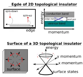
1.1.1 Topological Insulators
which occur due to the creation of a Dirac cone between the valence and conduction bands [14]. Example energy dispersion relations for both 2D and 3D TIs are shown in gure 1.1, along with schematic representations of the allowed electron motion. The link between spin and momentum means that if an electron was backscattered from an impurity then it would be required to reverse its spin. The reversal of an electrons spin is not allowed as this would break the time reversal symmetry of the system, and therefore TIs possess dissipationless transport along the surface [15]. This dissipationless transport is one of the main reasons that devices incorporating TIs are proposed to have lower power consumption when compared to standard electronics [2]. TIs could also be used for applications in quantum computing, where they would be used to create novel quasi-particles such as the Majorana fermion [16]. A promising candidate TI material that is of relevance to this thesis is Sb, which is discussed in more detail in section 1.2.1.
1.1.2 Half-metallic ferromagnets
Half metallic ferromagnets (HMFs) are a class of materials that are predicted to display 100% spin polarisation at the Fermi level [17]. This is because unlike standard semiconductors HMFs only possess a band gap in their density of states (DOS) at the Fermi energy for the minority spin direction (gure 1.2). This means HMFs behave as a conductor for one electron spin and as an insulator for the opposite spin.
Figure 1.2: Density of states (DOS) near the Fermi energy (Ef) for a semiconductor,
ferromagnetic metal and a half-metallic ferromagnet, showing the energy gap which occurs for one of the spin directions.
1.2 Material information
Having provided a brief review of TIs and HMFs, information regarding the specic materials studied in this thesis will be discussed. The work presented in this thesis is mainly concerned with surfaces and interfaces which display three-fold symmetry, specically (0001) planes of hexagonal materials and (111) planes of cubic materials.
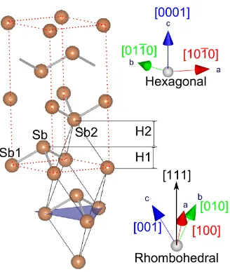
1.2.1 Sb
data.
[image:24.595.240.404.294.488.2]Publication a c H1 H2 Sb-Sb1 Sb-Sb2 Barrett et al. [28] 4.3084 11.274 1.506 2.251 2.908 3.355 Bengió et al. [29] 4.30 11.340 1.540 2.240 2.921 3.344 Materials Project [30] 4.3853 11.449 1.523 2.294 2.955 3.413
Table 1.1: Values reported for hexagonal Sb bulk crystal lattice parameters. All distances shown are in Å. H1 is the step height between nearest neighbours, H2 is the step height between second nearest neighbours. Sb-Sb1 is the bond distance between nearest neighbours. Sb-Sb2 is the bond distance between second nearest neighbours.
Figure 1.3: Crystal structure of bulk Sb, with the rhombohedral unit cell shown in solid black line and the hexagonal (111) unit cell shown in dotted red line.
There have been many research eorts investigating Sb thin lm growth over the past few decades, with a large proportion of this work focussing on the growth of Sb layers with coverages ≤1 monolayer (ML) [31] [32] [33]. While some of this
on (111) surfaces including Ge(111) [40] and GaSb(111) [41].
Other work has focussed on the use of Sb pre-deposition steps in the growth of nanostructures. For example, Kaizu et al. [42] studied (00L) crystal truncation rods (CTRs) for InAs quantum dot (QD) growth on GaAs(001), and found that an Sb-adsorbed layer led to Sb atoms diusing into the substrate up to a distance of 8 atomic layers, causing an increase in InAs QD density at the surface. Pillai et al. [43] have shown that Sb layers of 0.8-1.4 ML could be used to improve the interface of InAsSb/InAs(111) multi-quantum well structures.
Recent density functional theory (DFT) studies on Sb has focussed on the presence of topological surface states in Sb(111) surfaces [44][45]. Chuang et al. [46] showed that a topological insulating state can be induced in a single Sb BL with tensile strain. Wang et al. [47] also found that strain played an important role in the transition from 2D TI to trivial semiconductor. Lee et al. [48] performed DFT calculations for a 4-BL Sb lm and found that doping with non-magnetic impurity atoms could aid in achieving topological conduction. Zhang et al. [49] showed that for Sb lms ranging from roughly 1 nm to 8 nm, rst-principles calculations predict multiple transitions of electronic properties. Films of ≤1 nm were predicted to be
trivial semiconductors, lms 1 - 2.7 nm were predicted to exhibit the 2D quantum spin hall state, lms 2.7 - 7.8 nm were predicted to have topological insulating states, and lms >7.8 nm were predicted to behave as topological semimetals. A recent review of topological semimetals is available by Burkov [50], but this material class will not be discussed further.
aect the electronic properties of the Sb lms. For production of reliable Sb-based spintronic devices it is therefore vital to gain a better understanding of the growth of Sb ultra-thin lms ≤ 10 nm. Chapter 3 of this thesis presents results from a
surface x-ray diraction (SXRD) investigation on the growth of ultra-thin Sb lms on InAs(111)B substrates.
1.2.2 MnSb
MnSb belongs to a group of materials called transition metal pnictides (TMPs), which are compounds made from a transition metal and a group V atom. Some TMPs have been predicted to possess half-metallicity at room temperature for tetra-hedrally bonded structures [20]. They are also well suited to growth on standard III-V semiconductor materials via methods such as molecular beam epitaxy (MBE) [58] [59]. MnSb is a promising HMF spintronic candidate due to its high Curie temperature (TC = 587 K) and epitaxial compatibility with standard
Figure 1.4: Bulk structure of the three dierent polymorphs of MnSb.
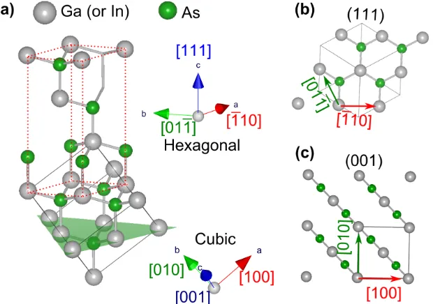
1.2.3 In1−xGaxAs
InAs and GaAs both adopt the zincblende bulk structure (cubic space group F 43m), which has a hexagonal unit cell in the [111] direction (gure 1.5). The tetrahedral bonding is asymmetric along the [111] direction, with each atom having three bonds in one direction and only one bond in the opposite direction. When a (111) surface is created the single bond will be preferentially broken which gives rise to two possible surface terminations. If the surface is terminated with the single broken bond on a group III atom then the surface is referred to as (111)A (gure 1.6a). However, if the surface is terminated with the single broken bond on a group V atom then the surface is referred to as (111)B (gure 1.6b). This dierence in terminating atomic species leads to large dierences in surface bonding chemistry and structure [65].
The identical structure of InAs and GaAs allows the formation of semicon-ductor alloys of the form InxGa1−xAs for use in the epitaxial growth of thin lms.
The in-plane lattice constant of these binary alloys can be calculated using Vegard's law (equation 1.1):
whereai is the in-plane lattice constant of material i. This enables tuning of
the lattice mismatch between overlayer and substrate by varying the ratio of In:Ga (i.e. altering the value ofx). InxGa1−xAs has been used in several spintronic research
eorts including spin distribution studies [66], spin injection eciency studies [67] [68], and mobility studies for spin transport applications [69]. Work presented in this thesis involves thin lm deposition using In1−xGaxAs substrates where x = 0,
0.5 or 1.
[image:28.595.163.478.275.493.2]Figure 1.5: (a) Structure of In(Ga)As with the cubic unit cell shown in solid black line, and the hexagonal (111) unit cell shown in dotted red line. Top two layers of the (b) (111)A , and (c) (001) surfaces.
1.3 Organisation of thesis
Chapter 2
Theory and Experimental
Methods
2.1 Molecular Beam Epitaxy
as the substrate (homoepitaxy) or a dierent material (heteroepitaxy).
Figure 2.1: Schematic representation of an MBE chamber. Dotted arrows are used to show motion paths of moveable components.
MBE allows the growth to be controlled to atomic layer precision. The growth of each atomic layer can be understood by considering a model of atomic processes (gure 2.2). In this model there are several interactions an adatom on the surface can undergo, it may join with other adatoms to form unstable subcritical clusters which can break apart back into individual atoms. The adatom can join critical clusters which only require one more atom to become a stable cluster. The adatom could also be captured by stable clusters already formed on the surface, or it could evaporate from the surface.
In heteroepitaxial growth (e.g. MnSb on GaAs) there may be a dierence in the lattice constant for the substrate (asub) and the layer (alayer). This denes the
lattice mismatch or mist strain (0) of the system using the following equation [71]:
0 =
asub−alayer
Figure 2.2: Steps of heterogeneous nucleation which occur in gas phase epitaxy (adapted from [72])
The elastic strain energy for a 2D layer of surface area S can be related to0 as a function of the layer thickness (h) [73]:
W2D =
E 1−ν
2
0Sh (2.2)
where E andν are the layer's Young's modulus and Poisson ratio respectively. For small layer thicknesses the thin lm structure can match the in-plane lattice spacing of the substrate, even if 0 is large (several %). A strained lattice-matched layer is often referred to as a pseudomorphic layer. Above a certain critical thickness the increase in elastic strain energy will become too large and strain relax-ation is required. This usually involves the introduction of mist dislocrelax-ations into the growing lm. Another method of relaxing the elastic strain is the formation of 3D islands, where free surfaces allow a decrease in the elastic energy [73].
which then coalesce (gure 2.3b). The third is the Stranski-Krastanov model where there is initially layer-by-layer growth, and then after a critical thickness the growth proceeds via 3D islands (gure 2.3c).
Figure 2.3: Growth models for deposition during MBE. (a)layer-by-layer growth (Frank-van der Merwe) (b)3D island growth (Volmer-Weber) (c) Initially layer-by-layer followed by 3D islands (Stranski-Krastanov)
A key parameter for growing compounds via MBE is the ux ratioJ, which for binary compounds can be dened as the ratio of the beam equivalent pressures (BEPs) of the two materials. For example, in the growth of MnSb J is calculated with the following equation:
JSb/M n= BEPSb
BEPM n (2.3)
Due to the cell conguration used on the MBE system at Warwick used in this work, when the Sb eusion cell shutters are initially opened there is a spike in Sb pressure which goes above the calibration pressure measured with the beam ux gauge. This can have a signicant eect on the ux ratio when growing thin samples with growth timestg≤3τ, whereτ is the time constant of the exponential decay for
the Sb eusion cell pressure. In order to account for this pressure burst a corrected ux ratioJSb/M ncorr can be calculated using equation 2.4 [74].
JSb/M nCorr =JSb/M n(
tg+ 32.929s
tg
2.2 Surface reconstruction notation
For a material with directional, covalent bulk bonds, the atoms present in the sur-face atomic layer possess dangling bonds which can cause the atoms to rearrange, adopting a dierent structure to the underlying bulk. This is called a surface re-construction, and can involve movement of the surface atoms both perpendicular and parallel to the surface in order for new bonds to be formed between atoms [75] In contrast, a surface relaxation is where atomic layers just have a change in their positions along the out-of-plane direction, with their in-plane positions remaining xed. In both cases, atomic re-arrangement acts to minimise the surface energy.
Surface reconstructions can be described using Wood notation, which denes the lengths of the surface mesh unit vectors for the reconstructed surface a0 and b0
relative to the lengths of the unit vectors for the underlying bulk-terminated surface mesh a and b. If the scaling between the unit vectors is given as |a0| = p|a| and |b0|=q|b|, then the general form of Wood notation is:
X{hkl}(p×q)Rφ−A
where X is the surface material,φis the angle between the two sets of surface mesh unit vectors and A is the adsorbate material (this term is only included if the surface atoms are adsorbates which dier from the surface material). Examples of Wood notation are shown in gure 2.4, highlighting the use of p to label primitive unit meshes andcto label centred unit meshes.
In the case where the directions of unit vectors a0 and b0 cannot be related
to a and b with a simple rotation and scaling, the matrix notationGmust be used as follows:
a0 =G
11a+G12b b0=G
G=
G11 G12 G21 G22
Note that a similar matrix notation can be used to describe the interface between two materials of dierent symmetry [76].
(a) (b)
Figure 2.4: Example surface reconstructions where circles represent the periodicity of the unreconstructed bulk, and crosses represent the periodicity in the reconstructed surface. (a) The surface mesh for the unreconstructed bulk is shown as a dotted line, the red dashed line shows the (√2×√2)R45◦ surface mesh, which can also be described with the centered c(2×2) surface mesh shown as a solid black line. (b) The surface mesh for the unreconstructed bulk is shown as a dotted line, due to having no atom at the centre the reconstruction is described as the primitivep(2×2) surface. Adapted from [77]
2.3 Crystallographic direction notation
Figure 2.5: A comparison between cubic Miller notation [hkl] and hexagonal Miller-Bravais notation [hkil]. Unit cells for the surfaces are shown in red solid lines.
2.4 Bulk diraction
A bulk crystal can be described using a combination of lattice vectors Rn which
connect unit cells, and the atom positions rj within the unit cell. When X-rays
with an incident wavevector ki are diracted by a bulk crystal that has lattice unit
vectors (a,b,c) there are only certain values of diracted wavevector kf that give rise
to constructive interference, and therefore measured intensity. The scattering vector Q=kf−kiis commonly used to describe diraction. The scattering amplitude from
the crystal can be written as the product of two summations: a sum over the unit cell and a sum over the lattice (equation 2.5). Herefj(Q) is the atomic scattering
factor of thejth atom in the unit cell.
Fcrystal(Q) = X
j
fj(Q) exp(iQ.rj)
X
n
exp(iQ.Rn) (2.5)
Q· a =2πh Q · b = 2πk Q· c = 2πl
where h,k and l are integers. These conditions are derived from a summa-tion of scattering amplitude contribusumma-tions from all atoms in the crystal lattice, and this will be explained in more detail in section 2.5.2. The values of Q that satisfy these conditions make up a lattice of points referred to as the reciprocal lattice, with each point being the result of threeδ functions (oneδ function for each lattice vector). The reciprocal lattice is dened by the three reciprocal lattice unit vectors a∗,b∗,c∗, which are related to the real lattice vectors by the following equations [77]:
a∗ = 2π (b×c)
a.(b×c) b
∗ = 2π (c×a)
a.(b×c) c
∗ = 2π (a×b)
a.(b×c)
Therefore constructive interference will only occur when Q is equal to a recip-rocal lattice vector ghkl. This condition is summarised with the following equations:
kf =ki+ghkl (2.6)
ghkl=ha∗+kb∗+lc∗ (2.7)
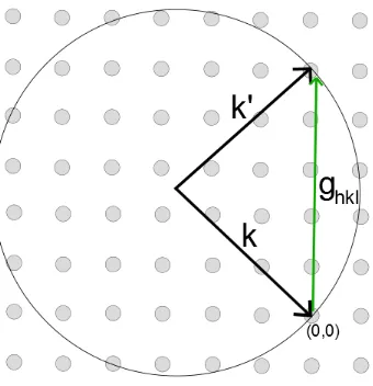
From knowing solutions to equations 2.6 and 2.7, the expected diraction pattern can be calculated graphically by constructing the Ewald sphere (Figure 2.6). The Ewald sphere has a radius |ki| and is centred on the tail of ki when the head
of ki is placed at the origin of reciprocal space. All points on the sphere's surface
represent values of kf, and there will only be diracted intensity when a point on
Figure 2.6: 2D representation of the construction of the Ewald sphere, with grey circles representing the reciprocal lattice. An example reciprocal lattice vector ghkl
is also shown.
2.5 Surface X-ray diraction
X-rays oer a very useful technique for probing the structure of materials due to having much weaker interactions with atoms compared to other probes such as elec-trons. This weak interacting nature allows X-rays to provide information on bulk materials and buried interfaces of samples. Surface sensitivity can be obtained by using an incident angle very close to the critical angle of the material being investi-gated. The critical angle (αc) of a material is linked to its refractive index through
equations 2.8 and 2.9 using the simplication thatβ=0.
n= 1−δ+iβ αc=
√
2δ (2.8)
δ = 2πρf 0(0)r
0
k2 β =
µ
2k (2.9)
angle belowαcis used, an evanescent wave is setup which propagates parallel to the
surface and decays rapidly into the sample. This can decrease the penetration depth of the X-rays to a few nanometers, boosting the signal from the sample surface [78]. When a low incident angle is used in scattering geometry the amount of active ma-terial being probed, and concomitantly the diracted signal strength, is signicantly decreased. For this reason surface X-ray diraction (SXRD) experiments using low incident angles require the use of synchrotron radiation X-ray sources that provide high enough intensities to obtain reliable counting statistics.
When considering X-rays being diracted by a 2D monolayer, the Laue con-dition in the direction perpendicular to the sample surface is relaxed. This means that only the component of kiparallel to the surface is conserved, and the equations
summarising the conditions on diraction become:
kfk =kik+ghk (2.10)
ghk=ha∗+kb∗ (2.11)
a∗ = 2π (b×n)
a.(b×n) b
∗ = 2π (n×a)
a.(b×n)
a plot of intensity versus Qz is related to the interfacial parameter between the
overlayer and substrate [75]. Examples of the eect that lattice displacements and surface roughness have on the shape of the [01L] CTR for a GaAs(111)B model are shown in gure 2.8.
Figure 2.7: Example reciprocal lattices for a 2D monolayer, a bulk crystal with a monolayer, and a real truncated crystal.
Figure 2.8: Changes in GaAs(111)B [01L] CTR as a result of (a) top layer displace-ment, and (b)surface model roughness or compression of top 12 atomic layers.
2.5.1 SXRD Data collection
of degrees of freedom for the detector [79]. SXRD experiments presented in this thesis were carried out at either the I07 bealime at Diamond Light Source (UK) [80] or the BL11XU beamline at SPring-8 (Japan) [81]. Experiments at the I07 beamline were performed in the second experimental hutch (EH2), using a (2+3) diractometer (gure 2.9). The UHV chamber in EH2 is made up of three separate sections; a pumped load lock, a pumped and ion-pumped buer chamber, and a turbo-pumped and ion-turbo-pumped analysis chamber. Experiments performed at BL11XU used a (2+4) diractometer with the azimuthal rotation of the detector xed, so it approximates a (2+3) diractometer setup. The UHV system on BL11XU has two chambers separated by a gate valve; a sample loading chamber, and a growth and analysis chamber. In both SXRD systems the sample was mounted in vertical scattering geometry, with the sample normal parallel to the oor.
Figure 2.9: Schematic representation of the diractometer at I07, Diamond light source (UK).
how the sample blocks the direct X-ray beam with all diractometer angles set to 0. For the crystallographic method, the sample is initially attened the same way but then a test reection is measured while the sample is rotated. Any slight o-set due to sample miscut will be seen as a movement of the signal upon azimuthal rotation of 180◦ about the surface normal, and can be corrected accordingly. Once
the sample is level a UB matrix needs to be assigned in order to allow navigation in reciprocal space. The UB matrix is a combination of two matrices; U and B. The B matrix is used to convert the reciprocal lattice of the sample to a Cartesian frame, and is obtained directly from the samples real space lattice (ai, αi) and reciprocal
space lattice (bi, βi) (equation 2.12). The U matrix is called the orientation matrix,
and accounts for the movement of the various diractometer circles and the sample positioning relative to the diractometer axis. This means that the value of the U matrix is dependent upon the diractometer type, as well as on what position the sample has been mounted in. The UB matrix is determined experimentally by measuring the positions of several reections. If the lattice parameters are known then only two reections from non-parallel planes are required. However, if the lattice parameters are unknown then the calculation requires measuring three reections which have reciprocal lattice vectors that are not co-planar [82].
B =
b1 b2cosβ3 b3cosβ2 0 b2sinβ3 −b3sinβ2cosα1
0 0 2π/a3
(2.12)
the out-of-plane direction, and has contributions from all material in the sample.
θ−2θ scans can be performed without a UB matrix, and only require the sample surface to be level. The UB matrix enables multiple other types of scans to be conducted, the most common types are crystal truncation rod (CTR) scans and HK-plane scans. CTR scans measure the change in intensity along the out-of-plane L direction when positioned at a specic HK value. CTRs only provide information on materials whose in-plane spacing is close to that of the material used to dene the UB matrix. HK-plane scans measure the change in intensity along any direction which lies in the HK plane, and provide information on the in-plane lattice spacings. HK-plane scans can only provide information on materials with similar symmetry to the material used to dene the UB matrix.
2.5.2 SXRD Data analysis
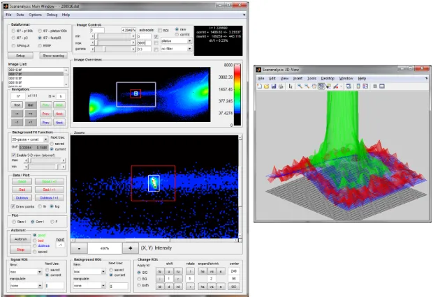
Once SXRD CTR data has been collected it needs to undergo data reduction and have correction factors applied before it can be tted to structural models. For SXRD analysis reported in this thesis a modied version of the matlab programme Scananlysis [83] was used to read in the Pilatus images collected during each scan and extract the integrated intensities. The analysis of an image can be quite a subjective process depending on the experience of the data analyst and the quality of the image. The general procedure followed for the datasets analysed in this thesis was as follows:
1. An appropriate region of interest (ROI) for the CTR signal was chosen, and it was ensured that the signal was centred within the ROI as this was necessary for implementation of L-shift corrections (detailed later in this section).
3. The simplest background tting function which achieved a reasonable t was chosen. Often this was a linear function when away from Bragg peaks and 2D gaussian function plus a constant when near to Bragg peaks.
4. Once a suitable background substraction was obtained the data point was marked as good and the analysis moved to next image repeating the procedure from step 1
[image:44.595.165.475.332.545.2]For the data analysis presented in this thesis there were a few instances where there were some exceptions to the standard protocol required, and these will be mentioned later on in this section.
Figure 2.10: Example printscreen from Scananalysis program, showing the main analysis window and the 3D plot of background tting.
Images that were taken very close to Bragg peaks (LBragg± 0.01) were
were further away from Bragg peaks but still in the vicinity (±0.05), whilst not being
very surface sensitive, still provided useful information for the scaling of CTRs. The modied Scananalysis software applied three correction factors to the data before saving the integrated intensity [83]. Firstly there is the polarisation factor which accounts for the polarisation of the incident X-ray beam given by:
Cp=ph(1−cos2δsin2γ) + (1−ph)(1−sin2δ) (2.13)
whereph is the horizontal polarisation of the synchrotron beam. The second
is a correction factor (CI) to account for the amount of CTR intercepting the Ewald
sphere given by:
CI = cosδsin(γ−α) (2.14)
Thirdly there is a correction factor to account for the active area of the sample [85]:
Cbeam=
1
sinδcos(α−βin) for non-specular CTR scans
sinα for specular CTR scans
These three correction factors are then used to calculate the corrected inten-sityIcorr from the recorded intensityIrec using:
Icorr =IrecCI
1 Cp
1
Cbeam (2.15)
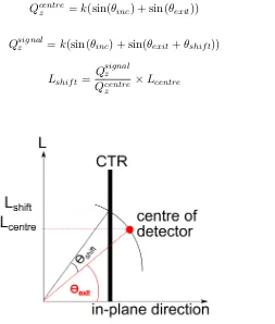
from the detector centre (gure 2.11). For most scans the direction of increasing L aligned with the horizontal line of the detector, however for a small number of scans the L direction was a diagonal direction in the detector reference frame. Therefore for these scans both the vertical and horizontal pixel distances from the centre were used. The pixel spacing was converted to an angular spacing (θshif t) which was used
to calculate the Qz value at the signal position (equation 2.17). This Qz position
was then used to calculate the shifted L-value using the equations 2.16 and 2.18.
Qcentrez =k(sin(θinc) + sin(θexit)) (2.16)
Qsignalz =k(sin(θinc) + sin(θexit+θshif t)) (2.17)
Lshif t=
Qsignalz
Qcentre z
[image:46.595.215.468.283.581.2]×Lcentre (2.18)
Figure 2.11: Diagram of L-shift calculations. The Matlab code used to implement this correction is included in Appendix A
Eects of crystallographic miscut
the L direction (gure 2.12). This altered direction of elongation results in a splitting of the CTR intensity so that there are two signals of intensity on the detector at the anti-Bragg positions. An example of this is shown in the lower panel of gure 2.12, showing the miscut CTR signal of a clean InAs(111)B surface at the (0 1 2.5) position. For samples with an o-cut a slightly altered approach to selecting the ROI and background boxes were needed due to there being two CTR signals present on the detector for the majority of the scan. For images where the two signals were close together a ROI box large enough to encompass both signals was selected and the pixel half-way between the two was used to calculate the L value. However when the two signals were further apart the background tting procedure struggled to correctly t the larger background area. Therefore for images that had two signals far apart a ROI box was selected that just encompassed the stronger of the two signals. Note that the o-cut aects quadrants of reciprocal space dierently, resulting in an inequivalence for CTRs which are usually symmetrically identical.
Figure 2.12: (a) Diagram of reciprocal lattice for a miscut surface, (b) an example detector image of a split signal. khigh
f (klowf ) is the upper (lower) limit of scattered
wavevector reaching the detector. The dotted elipses in (a) represent the elongation from a surface with no miscut.
CTR line prole tting programs
pre-sented in this thesis the program WinRod [86] was used. The theoretical model for SXRD can be derived using a kinematical approximation, where secondary dirac-tion events are neglected. The overall scattered intensity measured from a sample material for a specic hkl reection can be found by a succession of summations. This starts o by considering the X-ray intensity scattered from a single electron, goes on to sum these electron contributions over a single atom and then sums these atomic contribution over all the atoms present in the unit cell. Once the scattered intensity is obtained for a single unit cell, it is combined with the sample lattice type to obtain the hkl structure factorFhkl (equation 2.19). Here fj is the atomic
scattering factor of atomj,Bis the Debye-Waller parameter,Qis the total momen-tum transfer, (hkl) are the Miller indices, and (xyz) are the fractional co-ordinates representing the position of atom j. This structure factor is then used to calculate the overall scattered intensity|Fhkl|2.
Fhkl =
X
j
fjexp(
−BjQ2
16π2 ) exp(2πi(hxj +kyj+lzj)) (2.19) For the model used in the tting program WinROD a combination of a bulk slab dened by a bulk unit cell (B.U.C) and a surface slab dened by a surface unit cell (S.U.C) is used [87]. The structure factors of these two slabs are summed together to give the overall structure factor from the total sample (equation 2.20). The surface structure factor equation has an extra parameter for occupancy (θj)
because the surface atomic layers are not necessarily 100% occupied.
Fhkl =Fsum=Fsurf +Fbulk (2.20)
Fsurf =
S.U.C X
j
fjθjexp(
−BjQ2
Fbulk =
0
X
j=−∞
exp(2πilj) exp(jα) B.U.C X j
fjexp(
−BjQ2
16π2 ) exp(2πi(hxj+kyj+lzj))
(2.22) Bulk parameters were used to create an initial model with suitable starting atomic positions. The L-shifted CTR dataset was then loaded into the winROD program and compared to the calculated proles from a single bulk slab. Each CTR was individually scaled so that the intensities closest to the substrate Bragg points matched as closely as possible to the calculated proles from the bulk slab. Once all CTRs had been appropriately scaled, an initial surface slab using the appropriate bulk material atomic positions was added to the model and used as a starting point for structure renement. The structure renement process is carried out by using the simulated annealingχ2 minimisation procedure available in ROD. This returns aχ2 value (equation 2.23) which is used to quantify the goodness-of-t between the current model and experimental data. HereN is the number of data points in the dataset, p is the number of independent tting parameters used in the model, and σhkl is the experimental uncertainty.
χ2 = √ 1
N−p
X
hkl
|Fhklcalc|2− |Fexp hkl|2
σhkl (2.23)
Real world samples will most likely deviate from the simplied model pre-sented above. ROD has several modications which can be made to the interference sum in order to account for some of these non-ideal characteristics [87]. A roughness parameter R is included to account for surface roughness, which is calculated from the tted value ofβ, the value of the nearest Bragg peak (lBragg) and the number of
equidistant layers within the unit cell (Nlayers) (equation 2.24). For samples where
there are two dierent types of surface layer present ROD can have a second surface model loaded in as a set fraction (fs2) of the rst surface (fs). The modied equation
for Fsum is given in equation 2.25, where S is an overall scale factor and αj is the
R= s 1−β
(1−β)2+ 4βsin2π(l−lBragg) Nlayers
(2.24)
Fsum =SR
(1−fs)
X
j
αjFb,j2 +fs(1−fs2)
X
j
αj(Fs,j+Fb,j)2
+fsfs2
X
j
αj(Fs2,j+Fb,j)2
1/2 (2.25)
3D visualisation
3D visualisation of the CTR datasets was conducted using a combination of BINoc-ulars software [88] and Mayavi software [89]. While these software provided a useful method of visualising the dataset, it should be noted that their representation of the HK plane is not completely accurate as the HK axes should be separated by 60◦
rather than 90◦. Example Matlab code used to convert `.hdf5' les into `.VTK' les
is included in appendix A.
2.6 Reection high energy electron diraction
Figure 2.13: An annotated example of a RHEED pattern showing integer peaks, fractional peaks, Laue zones and Kikuchi lines
The RHEED pattern is displayed on a phosphor screen and provides infor-mation on the structure of the overlayer. An example RHEED pattern obtained from a highly crystalline (2×2) reconstructed surface is shown in gure 2.13. Both the integer and fractional signals are streaks, which arises from the intersection of the Ewald sphere by reciprocal rods of nite width (gure 2.14). These rods possess a nite width due to the imperfect periodicity of the sample surface and atomic vibrations [90]. The width of the reciprocal rod can also be aected by the spread in energies (∆E) of the electron beam, but a common tungsten lament produces
Figure 2.14: (a) Intersection of Ewald sphere with reciprocal rods of nite width, and (b) Corresponding streaks in real space on the RHEED phosphor screen.
The strong integer streaks correspond to distances of periodicity present in both the reconstructed surface and the unreconstructed layers beneath. The frac-tional order streaks between the integer order streaks correspond to the larger dis-tance of periodicity present in just the reconstructed surface. The example RHEED pattern (gure 2.13) also exhibits other common features including Laue zones and Kikuchi lines. Laue zones are extra bands of diracted intensity that arise from the Ewald sphere cutting through multiple planes of reciprocal rods. Kikuchi lines are a set of lines that intersect the central integer streak at roughly 45◦ that arise
due to secondary scattering eects. This is where inelastically scattered electrons within the crystal contribute to the diraction pattern by undergoing elastic scat-tering from bulk planes. Therefore Kikuchi lines indicate high crystalline quality of the overlayer.[90]
For surfaces which are almost perfectly periodic the reciprocal rods approach
δ functions, and produce a diraction pattern consisting of spots. This high level of periodicity occurs for surfaces which possess terraces of material≥100 nm in width.
growth is occurring via either Volmer-Weber or Stranski-Krastanov growth modes. If the transmission spots share the same spacing as the integer streaks then they are termed commensurate, but if they have a spacing that diers from the integer streak spacing then they are termed incommensurate.
Figure 2.15: Real space and reciprocal space diagrams for hexagonal surfaces, high-lighting the distances probed when used dierent RHEED directions.
For a hexagonal surface there are two dierent magnitudes of spacing, in di-rections which are 30◦ apart. To collect full two dimensional RHEED information
from these surfaces it is necessary to rotate the sample about its normal, due to the fact that any periodicity present in the plane of incidence will not aect the period-icity of the RHEED pattern [77]. The relationship between the real and reciprocal lattices for a hexagonal surface are shown in gure 2.15, with the RHEED pattern either being wide [10 10] or narrow [2 110]. The spacings of the real lattice can be calculated from either the wide or narrow patterns. For the wide RHEED pattern a simple factor of two is needed to transform the spacing d into the lattice constant a. For the narrow RHEED pattern a factor of 1/cos(φ) is needed where φ is the angle between the spacing being probed and the lattice parameter (e.g. 30◦ for a
hexagonal lattice)[90][91].
screen as calibration. From this relationship the real space distances being probed (d) can be calculated using the following equation:
d= 2πL kis
, (2.26)
where L is the distance from sample to the RHEED screen (camera length), s is the separation of the integer streaks in the RHEED pattern, and ki is the wavevector of
the incident electrons.
2.7 Low energy electron diraction
Low energy electron diraction (LEED) is a dierent UHV electron diraction tech-nique for measuring reciprocal space, which is conducted in backscattering geometry (gure 2.16). LEED is usually conducted with an electron beam accelerated with 10-500 V, which is incident normal to the surface with a uorescent screen collecting the elastically backscattered electrons [92]. Rotation of the sample is not required during LEED because each pattern provides a measurement of reciprocal space in two-dimensions, which are approximately in the HK plane.
2.8 X-ray Photoelectron Spectroscopy
X-ray photoelectron spectroscopy (XPS) is a technique which allows the identica-tion of atomic species and chemical environments present near a sample's surface. In XPS a monochromatic X-ray beam is incident on a sample surface resulting in the photoemission of electrons. The spectrum of photoelectron energies is measured, typically with a concentric hemispherical analyser. From knowing the initial energy of the X-ray photons (hν), the work function of the material (φ) and the kinetic en-ergy (EK) of the measured electrons, then the binding energy (EB) of the measured
electron can be calculated using the relation EK = hν−EB−φ. A typical X-ray
source is Al Kα , which has ahνvalue of 1486.7 eV. The exact values ofEB provides
information on both the atomic species present in a sample, as well as the chemical bonding environments of the atoms. Whilst the X-rays can penetrate ≥1 mm into
the sample, the photoelectrons produced have an inelastic mean free path of∼1nm.
This means that typically XPS measures photoelectrons from only the top few nm of a sample.
2.9 Atomic Force Microscopy
Atomic force microscopy (AFM) is an imaging technique which allows the measure-ment of local surface topography. In AFM a cantilever with a sharp tip is moved over a sample surface, and the interactions between the surface atoms and the tip cause changes in the deection of the cantilever (gure 2.17). The tip is scanned across the sample surface using piezo electric motors, and the movements of the cantilever are measured by the change in position of a laser beam reected onto a photo diode. These cantilever movements are then processed and used to build up a map of the surface topography, an example image is shown in the right panel of gure 2.17.
contact. The second is tapping mode where the cantilever is driven to oscillate at a set frequency, then the tip is scanned over the surface without making prolonged contact. The frequency of oscillation is altered by a magnitude determined by the interactions of the tip and the sample surface. In both modes a feedback system ensures that either the cantilever deection or frequency shift is kept constant as the tip is rastered, generating a surface topography z(x,y). The majority of AFM images in this thesis were collected using contact mode, and exceptions to this will be identied as they are presented. Typical image sizes are of the order 1µm, and typical root mean square (RMS) roughnesses are 1 - 10 nm
The program Gwyddion [93] was used to analyse all AFM images presented in this thesis. All images had a second order polynomical background removed to account for sample tilt and thermal drift.
Figure 2.17: (left) Schematic representation of an AFM (right) Example AFM image obtained using contact mode AFM.
2.10 Scanning Electron Microscopy
statistical information on the occurrence of surface features such as crystallites. In this work SEM is only used to assess the prevalence of particular features on MBE-grown samples. A full review of SEM methods can be found in [94].
2.11 Transmission Electron Microscopy
In transmission electron microscopy (TEM) an incident electron beam is transmitted through a very thin region of a specimen, and the transmitted electrons are detected. The thinned sample can be created by fabricating a specimen perpendicular to the sample surface, which allows the full depth of an MBE layer structure to be in-vestigated. This can provide information on the structure such as interface quality and layer homogeneity. High resolution imaging can readily provide information on individual atomic columns present in dierent layers of the substrate, as well as the formation of structures at interface e.g. steps.
When no optics are used to treat the transmitted electron beam a collec-tion of diraccollec-tion spots will be recorded, creating a selected area diraccollec-tion pattern (SADP). These spots correspond to allowed diraction conditions, and can be anal-ysed in a similar way to other diraction techniques. SADPs can complement other techniques by providing local information on crystal structures present within areas of the order 100 nm in size.
2.12 Vibrating sample magnetometry
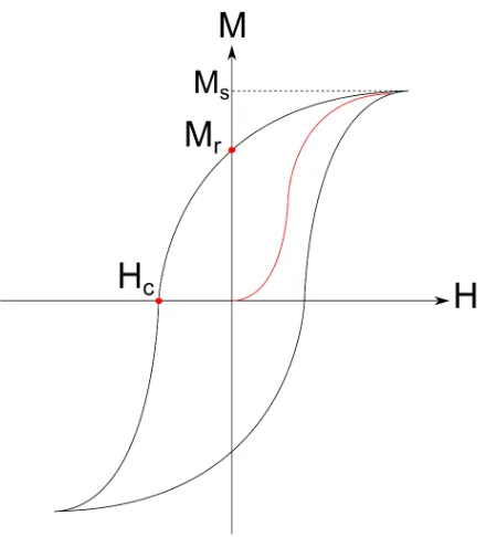
To assess the magnetic properties of MBE-grown thin lms, vibrating sample mag-netometry (VSM) was employed. In VSM a sample is placed between two coils of wire and subjected to an external magnetic eld (H ). The sample is then oscillated perpendicular to the common axis of the coils. The movement of the sample will induce a current in the coils determined by the samples magnetisation (M ). Mea-suring changes to the current induced in the coils when the value of H is altered will provide information on the magnetic behaviour of the sample. A M-H loop is the change in M measured when H undergoes one full oscillation between an upper and lower limit(gure 2.18). There are several key values which can be obtained from M-H loops. The saturation magnetisation (Ms) is the maximum value of M
obtained through the loop. The remnant magnetisation (Mr) is the magnetisation
which remains after the external eld is returned to 0. The coerceive eld (Hc) is
the eld required to return the magnetisation of the sample back to 0. Ms gives
in-formation on the overall magnetic quality of the sample, whereasMrandHcprovide
Figure 2.18: Schematic M-H loop with annotations showing the saturation magneti-sationMs, remnant magnetisationMrand coercive eld Hc. The red line shows the
Chapter 3
Ultra-thin Sb lm growth on
InAs(111)B
3.1 Introduction
Due to the theoretical predictions of possible topological surface states in Sb (see section 1.2.1), there has been renewed interest in understanding the growth of ultra-thin Sb lms with thicknesses≤10 nm. Depositions of Sb onto Si(001) have shown a
strong dependence on substrate temperature [95], with substrate temperatures below 300◦C producing a 2D Sb layer with clusters forming for coverages above 0.9 ML.
Use of higher substrate temperatures lead to the formation of just 2D layers with coverages 0.7-0.9 monolayers (ML), where the value of coverage depended on the substrate temperature and adsorbing species used (Sb4 or dissociated Sb4).
the same manner. The rst Sb BL deposited in a crystalline manner, the second to fourth BLs were amorphous, and the lms transitioned back to the crystalline phase on completion of the fth BL. Growth of thicker Sb(111) lms (10 - 500 Å) have been reported on Bi(111) through the use of SbxBi1−x buer layers formed by Sb
deposition at elevated temperatures [99].
Growth of Sb lms on III-V semiconductor surfaces has also been investi-gated, with initial research focussed on Sb growth on GaAs(110) nding that depo-sition at 300 K proceeds via monolayer-plus-multilayer simulataneous growth [100]. Cafolla et al. [101] used XPS studies to show that Sb deposition onto GaAs(111)B at room temperature follows Volmer-Weber growth characteristics. Carelli et al. [102] have also reported the creation of 2D Sb layers for Sb adsorption on GaAs(110), where a single Sb ML remained after a post-deposition anneal between 240-360◦C,
highlighting the strong bonding present between the rst Sb ML and the substrate. Initial studies on Sb thin lms grown at Warwick have looked at deposition of Sb onto various substrates including glass, InAs(111)B, GaAs(111)B and GaSb(111). It was found that InAs(111)B substrates have an excellent epitaxial match to Sb lms, with the thin lms also exhibiting anomalously high transport measurements. The increased mobility measured on these samples could be linked to topological surface states present in the Sb lm. An estimate of the critical thickness for the Sb/InAs(111)B system was calculated to be approximately 75 nm, and was obtained using the Matthews-Blakeslee model with a {11 22} slip plane in the <11 23> slip direction. This slip system was selected due to previous work by Srinivasan et al on similar hexagonal systems [103]. This critical thickness value shows that the system is well suited for ultra-thin lm growth studies.
InAs(111)B(1×1) surfaces was carried out. The results of this SXRD study will
be presented in this chapter as follows; experimental details of sample growth and characterisation will be given in sec. 3.2, results including XPS, SXRD and AFM will be presented in sec. 3.3, and a summary is then given in sec. 3.4.
3.2 Experimental details
SXRD experiments were performed on the I07 beamline at the Diamond Light Source synchrotron, Oxford UK. Deposition of Sb was achieved using an Sb Knudsen ef-fusion cell originally from Warwick attached onto the main XRD chamber of EH2. This Sb cell was calibrated using XPS and low energy electron diraction (LEED) measurements from a Ge(111) substrate test sample.
InAs(111)B samples 10 mm × 10 mm in size were mounted onto stainless
steel plates using Indium eutectic bonding. Once loaded into UHV the samples were degassed and then cleaned with cycles of argon ion bombardment (500 eV , discharge current 3mA, 8 minutes) and annealing (Tsub=410-440◦C for 30 minutes).
[image:62.595.242.401.518.676.2]This cleaning process produced a strong, sharp hexagonal LEED pattern (gure 3.1) which is consistent with LEED patterns from clean InAs(111)B reported in literature [104].
Figure 3.1: LEED pattern from a clean InAs(111)B-(1×1) surface, obtained using
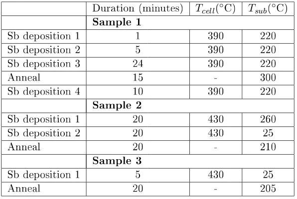
Three samples were grown using the experimental settings and procedures detailed in table 3.1. For the rst sample (sample 1) repeated depositions were conducted with the high substrate temperatureTsub= 220◦C. For the second sample
(sample 2) an increased Sb beam ux was used, and two stages of growth were carried out. The rst deposition on sample 2 was aiming for a similar growth rate to sample 1, consequently both the substrate temperature (Tsub) and the Sb eusion
cell temperature (Tcell) were increased. For the second deposition on sample 2 the
substrate temperature was reduced to room temperature. Sample 2 then underwent a post-deposition annealing stage for 20 minutes at Tsub = 210◦C. The nal sample
(sample 3) had only a single deposition stage usingTcell= 430◦C , with the substrate
kept at room temperature. Following this single stage deposition sample 3 was annealed atTsub = 205◦C for 20 minutes.
Duration (minutes) Tcell(◦C) Tsub(◦C)
Sample 1
Sb deposition 1 1 390 220
Sb deposition 2 5 390 220
Sb deposition 3 24 390 220
Anneal 15 - 300
Sb deposition 4 10 390 220 Sample 2
Sb deposition 1 20 430 260 Sb deposition 2 20 430 25
Anneal 20 - 210
Sample 3
Sb deposition 1 5 430 25
[image:63.595.172.470.372.572.2]Anneal 20 - 205
Table 3.1: Growth settings and procedures for all Sb/InAs(111)B samples. Tcell is
the temperature of the Sb eusion cell, andTsubis the temperature of the InAs(111)B
3.3 Results
3.3.1 XPS
Figure 3.2: XPS data collected from sample 1 after multiple depositions in the energy ranges of (left) Sb 3d signal, and (right) As 2p signal
Figure 3.5: XPS data collected from around the Sb 3d region for samples (a) S1 after deposition 3, (b) S2 after deposition 1, and (c) S3 after deposition 1. Red lines show full t prole, dashed grey lines show background function, and other colours of solid lines indicate pairs of doublet peaks tted to Sb 3d.
3.3.2 SXRD
All XRD data presented in this chapter was measured at the I07 beamline (Diamond Light Source, UK) using a photon energy of 12.5 keV (0.99Å), and recorded using a PILATUS 100K detector [105].
Out-of-plane symmetric XRD sample 1
strong InAs(111) Bragg peaks in order to avoid saturation of the detector. All scans taken after the initial Sb deposition (stages 2-4) are almost identical, which indicates that repeated depositions at high substrate temperature did not signicantly alter the sample surface. There is a broad feature labelled `1' present in all scans at approximately 2θ= 19.3◦ (lattice spacing 2.959Å), which becomes more pronounced in scans taken after the initial Sb deposition. A possible identity for this signal is the h-In(0001) reection (spacing of 2.964Å). Extra In at the surface is plausible due to the formation of excess group III atoms on III-V surfaces being well documented in literature [106] [107], where heating the substrate above the congruent temperature leads to a larger loss of the group V species. However, the signal's broadness and a lack of higher order reections means that a denitive identication is not possible.
![Figure 2.2: Steps of heterogeneous nucleation which occur in gas phase epitaxy(adapted from [72])](https://thumb-us.123doks.com/thumbv2/123dok_us/9459246.452725/32.595.121.517.104.290/figure-steps-heterogeneous-nucleation-occur-phase-epitaxy-adapted.webp)