163
©IJRASET: All Rights are Reserved
Designing of Parallel to Serial Converter and Flash
ADC using Reversible Gate
A Jonitha1, Prof. Dr R V S Satyanarayana2
1
Reg. 1116418, Final year M.Tech (communication Systems), Sri Venkateshwara University College of Engineering, Tirupati- 517502
2
ECE Department, Sri Venkateshwara University College of Engineering, Tirupati- 517502
Abstract: The Reversible Logic maps unique input to the output and ensure one to one mapping. This logic is used in emerging applications like low-power design, quantum computation, optical computing, bioinformatics and nanotechnologies. In communication between devices, the design of Parallel to Serial Converter plays an essential role as data bits in encoded form are transmitted serially rather than in parallel. This work understands and nurtures the necessity of reversible logic for future revolutionary computing and communication technologies. Among the reversible gates designed, Fredkin Gate is considered to be the universal gate which has a quantum cost of 5 and garbage outputs of 6. This work aims at reducing the quantum cost by using DRG4 Gates whose quantum cost is 4 and garbage outputs are 2. Using this reversible logic, the parallel to serial converter is designed to operate at 50MHz. The designs are coded in VHDL using structural modeling. These are synthesized and simulated in Xilinx ISE Design Suite 14.5. The results are compared for various parameters and the proposed design is found to be a better choice of implementing the parallel to serial converter practically due to less quantum cost, area, power dissipation, garbage outputs, etc. As a further extension work, the work is carried out for Analog to Digital Converter for Flash ADC and the proposed design is found to be a better choice to implement in Reversible Logic with less quantum cost, area, power dissipation, garbage outputs, etc.
I. INTRODUCTION
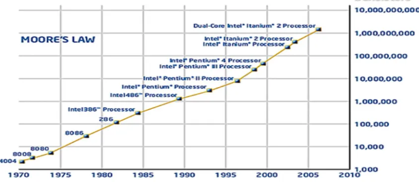
[image:1.612.104.526.529.713.2]The ever growing demand of high end computing applications has posed the challenge of continuous technology up gradation. The up gradation in technology has enabled the complex applications like Cloud computing, Real-time transitions on huge databases, Biotechnological computations a reality. Technological advancements in terms of higher operational frequency and miniaturization of chip in recent years have generated sufficient computing power to enable this growth. As predicted by Gordon Moore in 1960, popularly known as Moore’s law, the transistor count in a chip will be double every one and half year on the average. Transistor growth is shown by Gordon Moore in figure 1.1. ITRS (International Technology Roadmap for Semiconductors) has also drawn a road-map of required feature size in future at atomic level in 2050. Shrinking in feature size resulted in a number of implementation and operational difficulties like heat dissipation, requirement of very thin laser beam, clock distribution etc.
164
©IJRASET: All Rights are Reserved
Current technologies are finding it difficult to continue with the required level of growth. Alternative technologies are emerging to take place so that the growth momentum can be continued. Reversible computing is one of the computing system in which new generation computing system can be designed. Because of its basic nature of reversibility, it retains the old information and reduces dissipation of heat in its operation.
II. LITERATURE SURVEY
Reversible computing is emerging as a potential development platform to replace conventional logic. Here represents previous work on reversible logic.
A. Reversible Logic Gates
Right from the stored program architecture given by John Von Neumann in 1949, heat dissipation per computation of bit is being estimated. R. Landauer [1961] pointed out that the irreversible erasure of a bit of information consumes power and dissipates heat. While reversible designs avoid this aspect of power dissipation. Destruction of bits causes heat dissipation as per Landauer Principle. Bannett in 1973 proposed a turning machine for loss-less computation by making it reversible. The development of reversible gates and circuits started after Toffoli proposed reversible logic gates in 1977. A number of gates have been proposed thereafter. The same has been described two categories namely basic gates and generalized gates.
Two constraints for reversible logic synthesis are:
1) Feedback is not allowed
2) Fan-out is not allowed (i.e., fan-out = 1).
A gate with k inputs and k outputs is called a k*k gate. Several reversible gates have been proposed over the last decades.
B. Reversible Circuit Design
Toffoli, Fredkin and Peres have given their reversible gates in 1980’s; these gates are used to implement the Boolean functions. Network of reversible gates to implement the specific Boolean function is called reversible circuits. Formally a combinational reversible circuit is an acyclic combinational logic circuit in which all gates are reversible and interconnected without explicit fan-out’s and loops.
III. OBJECTIVES
A. Multiple Comparative Analyses of Reversible Gates for Designing Logic Circuits
B. Designing parallel to serial converter using DRG4 gate
C. Designing of ADC convertor using DRG4_ gate
IV. FREDKIN GATE
The Fredkin gate (also CSWAP gate) is a computational circuit suitable for reversible computing, invented by Edward Fredkin. It is
universal, which means that any logical or arithmetic operation can be constructed entirely of Fredkin gates. The Fredkin gate is a circuit or device with three inputs and three outputs that transmits the first bit unchanged and swaps the last two bits if, and only if, the first bit is 1.
Fig No. 2 Circuit representation of Fredkin gate
The basic Fredkin gate is a controlled swap gate that maps three inputs (C, I1, I2) onto three outputs (C, O1, O2). The C input is
mapped directly to the C output. If C = 0, no swap is performed; I1 maps to O1, and I2 maps to O2. Otherwise, the two outputs are
swapped so that I1 maps to O2, and I2 maps to O1. It is easy to see that this circuit is reversible, i.e., "undoes" itself when run
backwards. A generalized n×n Fredkin gate passes its first n-2 inputs unchanged to the corresponding outputs, and swaps its last two
outputs if and only if the first n-2 inputs are all 1. The Fredkin gate is the reversible three-bit gate that swaps the last two bits if, and
165
©IJRASET: All Rights are Reserved
A. Reversible Logic based Parallel to Serial Converter Design
The three bit counter is constructed with the help of three toggle flip-flops. A variety of counter circuits of various types of complexities are viable in IC form. The design of Reversible T-Latch is carried out the combination of Peres Gate and Feynman Gate as shown in figure 2.5.
[image:3.612.80.534.369.679.2]The higher order design of 32-bit Parallel to Serial Bit conversion is performed in this work by using DRG4 Gate. The 32-bit multiplexer is designed as shown in figure 2.4.
Figure 3: Design of 32-Bit Multiplexer using DRG4 Gate
Figure 4: Design of Parallel to Serial Converter using Reversible T-Latches and DRG4 Gate based 32x1 Multiplexer.
166
©IJRASET: All Rights are Reserved
V. SYNTHESIS RESULTS
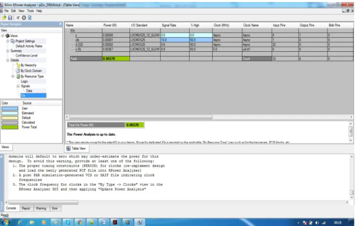
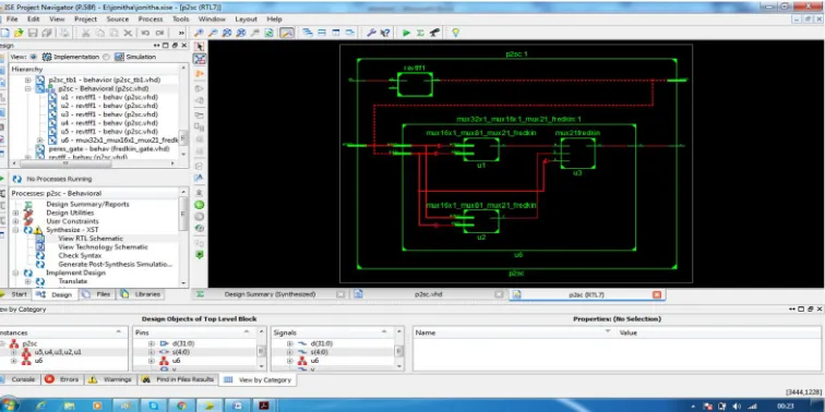
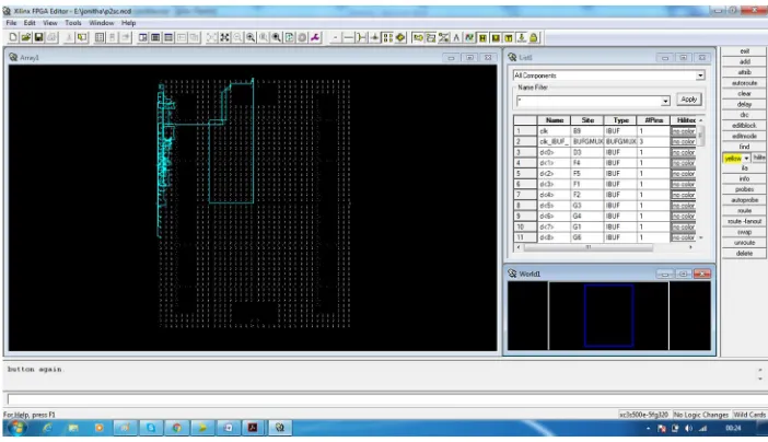
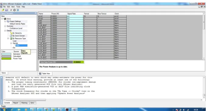
[image:4.612.128.486.113.303.2]The synthesis results include Design Summary, RTL Schematic, Technology Schematic, FPGA Floorplan and Routing and Power Analysis Report for Parallel to Serial Converter using DRG4 Gate as shown in figures 5 to 13.
[image:4.612.130.485.326.493.2]Figure 5: Design Summary of Parallel to serial converter using DRG4 gate
Figure 6: RTL Schematic of Parallel to Serial Converter using DRG4 gate
[image:4.612.132.482.517.716.2]167
©IJRASET: All Rights are Reserved
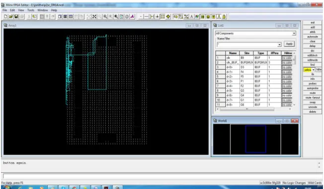
[image:5.612.144.470.75.266.2]Figure 8: Floor plan and Routed Design of Parallel to Serial Converter using DRG4 gate
Figure 9: Power Report Summary of Parallel to Serial Converter using DRG4 gate
[image:5.612.123.490.510.721.2]168
[image:6.612.142.473.76.240.2]©IJRASET: All Rights are Reserved
[image:6.612.135.477.264.473.2]Figure 11: Logic Power of Parallel to Serial Converter using DRG4 gate
Figure 12: Data Power of Parallel to Serial Converter using DRG4 gate
[image:6.612.130.486.496.721.2]169
©IJRASET: All Rights are Reserved
[image:7.612.132.484.102.301.2]The synthesis results include Design Summary, RTL Schematic, Technology Schematic, FPGA Floor plan and Routing and Power Analysis Report for Parallel to Serial Converter using Fredkin Gate as shown in figures 14 to 22.
[image:7.612.119.497.327.516.2]Figure 14: Design Summary of Parallel to Serial Converter using Fredkin Gate
Figure 15: RTL Schematic of Parallel to Serial Converter using Fredkin gate
[image:7.612.133.480.541.713.2]170
©IJRASET: All Rights are Reserved
Figure 17: Floor plan and Routed Design of Parallel to Serial Converter using Fredkin Gate
[image:8.612.130.481.75.277.2]Figure 18: Power Report Summary of Parallel to Serial Converter using Fredkin Gate
171
[image:9.612.137.477.75.266.2]©IJRASET: All Rights are Reserved
[image:9.612.137.477.290.473.2]Figure 20: Logic Power of Parallel to Serial Converter using Fredkin Gate
Figure 21 Signal Power of Parallel to Serial Converter using Fredkin Gate
[image:9.612.137.479.499.720.2]172
©IJRASET: All Rights are Reserved
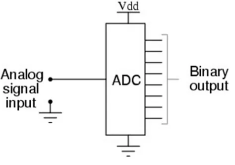
VI. INTRODUCTION TO ADC
An ADC converts a continuous-time and continuous-amplitude analog signal to a discrete-time and discrete-amplitude digital signal and is chosen to match the bandwidth and required SNR of the signal to be digitized. If an ADC operates at a sampling rate greater
than twice the bandwidth of the signal, then per the Nyquist–Shannon sampling theorem, perfect reconstruction is possible. The
presence of quantization error limits the SNR of even an ideal ADC. However, if the SNR of the ADC exceeds that of the input signal, its effects may be neglected resulting in an essentially perfect digital representation of the analog input signal.
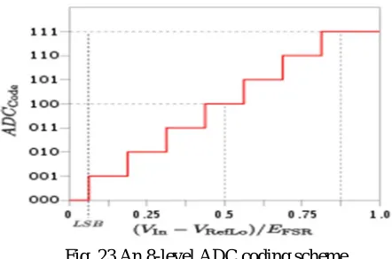
[image:10.612.190.411.191.337.2]A. Resolution
Fig. 23 An 8-level ADC coding scheme
The resolution of the converter indicates the number of discrete values it can produce over the range of analog values. The
resolution determines the magnitude of the quantization error and therefore determines the maximum possible average
signal-to-noise ratio for an ideal ADC without the use of oversampling.
B. Quantization Error
Quantization error is the noise introduced by quantization in an ideal ADC. It is a rounding error between the analog input voltage to the ADC and the output digitized value. The noise is non-linear and signal-dependent. In an ideal analog-to-digital converter, where
the quantization error is uniformly distributed between −1/2 LSB and +1/2 LSB, and the signal has a uniform distribution covering
all quantization levels, the Signal-to-quantization-noise ratio (SQNR) can be calculated from Where Q is the number of quantization bits.
C. Accuracy
An ADC has several sources of errors. Quantization error and (assuming the ADC is intended to be linear) non-linearity are intrinsic to any analog-to-digital conversion. These errors are measured in a unit called the least significant bit (LSB). In the above example of an eight-bit ADC, an error of one LSB is 1/256 of the full signal range, or about 0.4%.
D. Electronic Symbol
173
©IJRASET: All Rights are Reserved
VII. SIMULATION RESULTS OF ADC CONVERTOR
[image:11.612.190.427.79.245.2]The synthesis results include Design Summary, RTL Schematic, Technology Schematic, FPGA Floorplan and Routing and Power Analysis Report for Parallel to Serial Converter using DRG4 Gate as shown in figures 24 to 31
Fig 24: ADC DRG4_Gate Circuit
[image:11.612.70.541.288.731.2]174
©IJRASET: All Rights are Reserved
[image:12.612.67.543.53.717.2]Fig 26: Values of ADC convertor
Fig 27: Values of ADC convertor Design Summary Values
[image:12.612.63.547.457.712.2]175
©IJRASET: All Rights are Reserved
Fig 29 Outputs of ADC convertor
[image:13.612.73.535.47.723.2]Fig 30 Output of ADC convertor
176
©IJRASET: All Rights are Reserved
VIII. CONCLUSIONS
With the advancement of technology, there has been more and more need for the gigabit rate link for storage application, data communication, computer networks and etc. To meet with the high processing multi-gigabit speeds and system performance, it becomes necessary to have prompt and efficient high-speed inter-connects. Traditional parallel link has been used in circuits for a long time, which let the data be sent over multiple channels simultaneously. A Serial Data link is preferred for long distance communication. This work verifies the design of parallel to serial converter using reversible logic gates like Fredkin Gate, Peres Gate, Feynman Gate and DRG4 Gates. The designs are coded in VHDL using structural modelling. These are synthesized and simulated in Xilinx ISE Design Suite 14.5. The results are compared for various parameters and the proposed design i.e., by using DRG4 gate is found to be a better choice of implementing the parallel to serial converter practically due to less quantum cost, area, power dissipation, garbage outputs, etc. As it reduces the quantum cost by 15% and Garbage outputs by 5%. Further as an application, the designs are developed for Flash Analog to Digital Converter for which the proposed design proved to be better choice of implementation using Reversible Logic with an improvement of design in terms of quantum cost and garbage outputs.
REFERENCES
[1] Stephen Alexander Chin, Jason Luu, Safeen Huda, and Jason H. Anderson, " Hybrid LUT/Multiplexer FPGA Logic Architectures" IEEE Transactions on Very Large Scale Integration (VLSI) Systems, pp. 1-13,2015.
[2] International Technology Roadmap for Semiconductors (ITRS), http://www.itrs.net, 2016.
[3] Himanshu Thapliyal, Nagarajan Ranganathan, ”Reversible Logic : Fundamentals and Applications in Ultra-Low Power, Fault Testing and Emerging Nanotechnologies and Challenges in Future” 25th International Conference on VLSI Design, IEEE Computer
Society, pp13-15, 2012.
[4] Gordon Moore, “The Future of Integrated Electronics.” Fairchild Semiconductor Internal Publication”, Vol. 38, No. 8, April 1965.
[5] Dr. Mike Frank, “Quantum Computer Architectures for Physical Simulations”, James H. Simons Conferences on Quantum Computation for Physical Modelling Work-shop, University of Florida, May 2002.
[6] Hugo De Garis, Thayne Batty, “Robust, Reversible, Nano-scale, Femto-Second Switching circuits and their evolution”, Proceedings of the 2004 congress on evolutionary computation, XXX-2371, ISBN 0-7803-8515-2, IEEE, 2004.
[7] Michael P. Frank, “ The Physical Limits Of Computing”, Vol. 4, No. 3, pp. 16-26, May June 2002, doi:10.1109/5992.998637, IEEE, 2002.
[8] Robert Wille, “Introduction to Reversible Circuit Design”, Electronics, Communication and Photonics Conference (SIECPC), 2011 Saudi International, E-ISBN: 978-1-4577 0067- 5, Print-E-ISBN: 978-1-4577-0068-2, IEEE, 2011.