Design, Fabrication, and Characterization
of 3D Nanolattice Photonic Crystals for
Bandgap and Refractive Index Engineering
Thesis by
Victoria F. Chernow
In Partial Fulfillment of the Requirements for
the degree of
Doctor of Philosophy
CALIFORNIA INSTITUTE OF TECHNOLOGY
Pasadena, California
2018
i
ii
Acknowledgments
Caltech is an extraordinary institution, and I am grateful to have spent my graduate career here. It has been a privilege to be a part of such an inspiring community where curiosity and the pursuit of knowledge is foremost and constant. There are few places that can provide the kinds of opportunities and experiences I have been afforded here, and the people I’ve met throughout my time at Caltech have been truly amazing, indelibly helping to shape the person I’ve become.
I would like to thank my academic advisor, Professor Julia R. Greer, for her encouragement and constant support through the Ph.D. process. Julia has been singular in her enthusiasm and a primary reason for my choosing to come to Caltech. Upon joining her research group, I was given the structure and intellectual freedom needed to pursue my own research direction, and work in an area that was both unique to my previous experiences and academically stimulating. She has been incredibly supportive in allowing me to tailor my graduate school experience and explore opportunities outside of research. She has been instrumental in my coming to understand my strengths as a researcher, helped me work on my weaknesses, and aided in my discovery of what I love about the scientific process. I am thankful for the resources she has provided to allow me to develop technical and communication skills. Her encouragement to attend conferences has given me the opportunity to present my work, interface and learn from people in a variety of different fields, and create meaningful connections with individuals from all over the world. As I venture into the world outside of academia and graduate school, I know I will continue to use the presentation, communication, and critical thinking skills that Julia has been instrumental in helping me develop.
Thank you to the Dow Resnick grant for financially supporting my research, and the other funding sources which made this work possible.
iii student. I am incredibly indebted to Professor Rossman for all his help with FTIR and Raman characterization, as well as his scientific expertise and fantastic stories.
The work described this thesis required the use of numerous labs and user facilities throughout Caltech. I am especially grateful for the resources available through the Kavli Nanoscience Institute (KNI). The KNI cleanroom facilities made so much of my work possible, and KNI staff was invaluable in helping me to use and master a number of fabrication and characterization tools. In particular, I would like to thank Matthew Sullivan Hunt and Melissa Melendes. Matt has been an incredible resource for all things SEM and FIB related, and I am grateful for his compassion in listening to the various tribulations and joys of my day. During her time with the KNI, Melissa was the gatekeeper and master user of a plethora of tools, and I am thankful for her excellent training and cheerful disposition in all situations. I am very grateful to the Atwater group for their willingness to share lab resources and to the numerous graduate students who work so hard maintaining equipment and training others. In particular, I would like to thank Dr. Siying Peng for her help and training in using the angle resolved spectroscopy setup she custom built—Siying was an amazing resource for discussing the physics of photonic crystals and methodologies for studying these structures.
Thank you to Professor Jennifer A. Dionne and Dr. Hadiseh Alaeian at Stanford University for being exceptional collaborators on my first graduate research project. Thank you to Dr. Katherine Fountaine, Dr. Philip Hon, and Georgia Papadakis for your insights and all the scientific discussions which made the work in Chapter 4 possible.
iv Mike, Dylan, Namita, Jan, Andrey, and all Greer group members past and present – time spent with you inside and outside the lab was central to what made my Caltech experience so memorable.
Thank you to Jane Herriman, Georgia Papadakis, and Heather Duckworth. You inspire me with your intellect, ambition, and ingenuity. In times of triumph, and inevitable graduate school melancholy, I am so grateful to have been able to turn to you for encouragement and counsel.
I’d like thank the whole of Ruddock for being a home away from home for two memorable years. Getting to know you all, and gaining an insight into undergraduate life at Caltech, has been an awesome experience. Thank you to the whole RA team for being so incredible. And thank you to everyone on the Caltech Ballroom Dance Club for being the best group on campus and providing me with a creative outlet, as well as a great group of friends.
v
Abstract
vi
Published Content and Contributions
Chapter 2 is adapted from:
1) V.F. Chernow, H. Alaeian, J.A. Dionne, J.R. Greer. “Polymer lattices as mechanically tunable 3-dimensional photonic crystals operating in the infrared.” Appl. Phys. Lett. 107, 101905 (2015). DOI: 10.1063/1.4930819
V.F.C. designed, fabricated, and characterized samples (TPL DLW, SEM, FTIR), performed compression experiments, analyzed data, performed cell pathlength calculations, and wrote the manuscript.
Chapter 4 is adapted from:
2) V.F. Chernow, R.C. Ng, J.R. Greer. “Designing core-shell 3D photonic crystal lattices for negative refraction.” in Proc. SPIE (eds. Adibi, A., Lin, S.-Y. & Scherer, A.) 1, 101120G (2017). DOI: 10.1117/12.2251545
V.F.C. designed and performed plane wave expansion method simulations, analyzed data, fabricated samples (TPL DLW and O2 plasma etching), and wrote the manuscript.
3) V.F. Chernow, R.C. Ng, S. Peng, H.A. Atwater, J.R. Greer. “Dispersion mapping in 3D core-shell photonic crystal lattices” (in preparation).
vii
TABLE OF CONTENTS
Acknowledgments ... ii
Abstract ... v
Published Content and Contributions ... vi
List of Figures ... x
List of Tables ... xi
Chapter 1: Introduction to 3D Periodic Architectures as Photonic Crystals ... 1
1.1. Outline and Objectives ... 1
1.2. A Brief Introduction to Photonic Crystals ... 2
1.2.1. A Concise Overview of Photonic Crystal Theory ... 3
Chapter 2: Exploring the Photonic Band Gap Properties of 3D Periodic Architectures – Tuning Band Gap Position with Mechanical Strain ... 5
2.1. Introduction and Motivation ... 5
2.2. Fabrication of 3D lattices ... 6
2.2.1. Two Photon Lithography Direct Laser Writing (TPL DLW) ... 6
2.3. Mechanical Characterization of 3D Polymer Octahedron Nanolattices ... 8
2.3.1. Exploring Polymer Nanolattice Recoverability ... 8
2.3. Optical Characterization of Angle-Varied Nanolattices ... 9
2.3.1. Discussion of Stopband Position versus Effective Strain ... 10
2.4. Optical Characterization of in-situ Strained Nanolattices ... 12
2.4.1. Compression Cell Fabrication ... 13
2.5. Results and Discussion of Band Gap Tuning using Mechanical Strain ... 15
2.5.1. Calculating Compression Cell Pathlength Using the Interference Fringe Method ... 17
2.6. Comparison of Experimental Bandgap Position and Simulated Bandgap Results ... 19
2.7. Conclusions and Evolved Critiques ... 22
Chapter 3: Exploring the Photonic Band Gap Properties of 3D Periodic Architectures – Band Gap Properties as a Function of 3D Periodic Architecture ... 23
3.1. Outline and Motivation ... 23
3.2. Introduction to Periodic Lattice Architectures ... 23
3.2.1. Simple Cubic, Face Centered Cubic, and Base Centered Cubic 3D PhCs ... 23
3.3. Fabrication of 3D Nanolattices PhCs ... 27
3.4. Optical characterization of Octahedron, Octet, and Tetrakaidecahedron Nanolattices PhCs ... 29
3.4.1. Reflectivity Spectra with respect to Geometry and Periodicity ... 29
3.5. Comparing Experimental Reflectivity to Calculated Photonic Band Structure ... 31
viii
3.5.2. Direct Comparison of Peak Reflectivity and Bandgap Position ... 35
3.5.3. Comparing the FWHM of Reflectivity Peaks to Calculated Bandgap Width ... 39
3.6. Future Directions for Exploring the Photonic Properties of Polymer 3D Architected PhCs ... 42
Chapter 4: Exploring the Band Structure and Band Dispersion Phenomena of 3D Periodic Architectures – Demonstrating Negative Refraction in 3D Photonic Crystal Lattices ... 44
4.1. Introduction and Motivation ... 44
4.1.1. Photonic Crystal Bands and Equi-frequency contours (EFCs) ... 44
4.2. Negative Refraction and its Implications ... 45
4.2.1. Negative Refraction in metamaterials ... 45
4.2.2. Negative Refraction in Photonic Crystals ... 46
4.3. Photonic Band Structure and Equi-frequency Contour Calculations ... 47
4.3.1. Exploring Varied Simulation Parameters: Fill Fraction ... 49
4.3.2. The Effect of Relative Index of Refraction ... 51
4.3.2.1. Polymer Core, Ge Shell PhCs ... 51
4.3.2.2. Carbon Core, Ge Shell PhCs ... 54
4.3.2.3. Polymer Core, Si Shell PhCs ... 55
4.3.3. The Effect of Beam Ellipticity ... 57
4.3.4. The Effect of Shell Offset Relative to Core Position ... 59
4.3.5. The AANR Region and Experimental Observation of Negative Refraction ... 61
4.4. Core-Shell Photonic Crystal Fabrication ... 62
4.4.1. TPL DLW process ... 62
4.4.2. Discussion of Surface Symmetry Effects and Lattice Orientation ... 63
4.4.3. O2 plasma Etching ... 65
4.4.4. Germanium Deposition via Sputtering... 66
4.4.5. FIB cross-section characterization of Ge deposition on 3D structures ... 67
4.5. Optical Characterization of Core-Shell Photonic Crystal Lattices... 68
4.5.1. Fourier Transform Infrared Spectroscopy ... 68
4.5.2. Angle resolved Infrared Spectroscopy for Band Mapping... 69
4.5.3. Experimental Observation of a Photonic Band Relevant for Negative Refraction ... 71
4.5.4. Comparison of Experimental Band Structure and PWE Simulation Results ... 72
4.6. Conclusions and Outlook on Negative Refraction with 3D PhCs ... 74
4.6.1. Creation of a 3D Core-Shell PhC Superlens ... 74
Chapter 5. Perspectives on Future Research Directions for 3D Photonics ... 77
5.1. Opportunities in PhC Architecture and Topology ... 77
5.1.1. Topological Photonics... 78
ix
5.2. Future Directions for Index of Refraction Engineering and 3D Photonic Crystal Fabrication ... 80
Appendicies... 84
Appendix A. ... 84
Appendix B. ... 86
Appendix C. ... 88
x
LIST OF FIGURES
Figure 1. Process flow for the fabrication of 3D polymer nano and micro-architected structures ... 6
Figure 2. Scanning electron microscopy (SEM) images of a representative as-fabricated octahedron nanolattice. ... 8
Figure 3.Representative stress-strain data for a uniaxial compression of an octahedron nanolattice.. ... 9
Figure 4. Schematic showing the configuration of the Cassegrain lens used in the Nicolet Continuum Infrared Microscope in reflection mode. ... 10
Figure 5. The relationship between effective strain and stopband position in as-fabricated angle varied nanolattices ... 11
Figure 6. Schematic of the nanolattice compression cell setup. ... 13
Figure 7. Scanning electron microscopy (SEM) images of representative compression cell samples.. ... 14
Figure 8. Normalized reflectance spectra for an as-fabricated nanolattice outside of the compression cell (red), and under compression (blue) using the custom FTIR compression cell setup. ... 15
Figure 9. Strain-stopband plots comparing data from the as-fabricated angle-varied lattices under corresponding effective strain, and experimentally strained nanolattices using a compression cell over multiple cycles. ... 16
Figure 10. FTIR spectra of a background collected against a regular polished silicon surface, and a background collected against the bottom of an empty etched silicon well through a KBr window. .. 18
Figure 11. Results of simulated reflectance for effectively strained nanolattices compared to experimental data.. ... 20
Figure 12. A color map depicting the variation in reflection as a function of incident angle and wavelength for a simulated 45° nanolattice. ... 22
Figure 13. Schematic of an octahedron simple cubic PhC lattice. ... 25
Figure 14. Schematic of an octet face centered cubic PhC lattice ... 26
Figure 15. Schematic of a tetrakaidecahedron base centered cubic PhC lattice. ... 26
Figure 16. Representative images of as-fabricated octahedron, octet, and tetrakaidecahedron PhC lattices ... 28
Figure 17. FTIR reflectance spectra for octahedron, octet, and tetrakaidecahedron nanolattice PhCs.. ... 30
Figure 18. Brillouin zone and band structure calculated for the octahedron simple cubic lattice ... 32
Figure 19. Brillouin zone and band structure calculated for the octet face centered cubic lattice. ... 33
Figure 20. Brillouin zone and band structure calculated for the tetrakaidecahedron base centered cubic lattice. ... 34
Figure 21. Calculated bands and experimental reflectivity peaks for simple cubic octahedron nanolattice PhCs. ... 36
Figure 22. Calculated bands and experimental reflectivity peaks for face centered cubic octet nanolattice PhCs. ... 37
Figure 23. Calculated bands and experimental reflectivity peaks for base centered cubic tetrakaidecahedron nanolattice PhCs.. ... 38
Figure 24. Outline for comparing the FWHM of experimental reflectivity peaks to the calculated bandgap width Δω ... 40
Figure 25. FWHM of experimental reflectivity peaks versus calculated bandgap width Δω for octahedron, octet, and tetrkaidecahedron PhCs of varying periodicity. ... 41
Figure 26. CAD schematic of the 3D bcc PhC lattice... 48
Figure 27. Representative band structure and equifrequency contours. ... 49
xi Figure 29. Average AANR Frequency, AANR Frequency range, and equi-frequency contours for
polymer-germanium core-shell PhCs. ... 53 Figure 30. Average AANR Frequency and AANR Frequency range for amorphous carbon-germanium
core-shell PhCs. ... 55 Figure 31. Average AANR Frequency, AANR Frequency range, and equi-frequency contours for
polymer-silicon core-shell PhCs.. ... 56 Figure 32. Average AANR Frequency, AANR Frequency range, and evolution of band structure for
polymer-germanium core-shell PhCs with beams of varying ellipticity. ... 59 Figure 33. Examples of Ge-shell offset from the polymer-core center position in the X, XZ, and XYZ
dimensions, and the effects of shell offset on average AANR Frequency and AANR Frequency range. ... 61 Figure 34. Surface symmetry and orientation of the bcc PhC lattice. ... 63 Figure 35. Representative scanning electron microscopy (SEM) image of the (101) lattice face of a bcc
PhC lattice after 45 min of oxygen-plasma etching. ... 66 Figure 36. Scanning electron microscope images of a polymer-germanium core-shell PhC. ... 67 Figure 37. Normalized FTIR reflectance spectra for the polymer-Ge core-shell bcc PhC lattice compared
to reflectance from an IP-Dip polymer thin film. ... 69 Figure 38. Schematic of the orientation of incident QCL laser light relative to the PhC sample orientation
... 70 Figure 39. Experimentally measured and calculated band structure for the core-shell PhC lattice. ... 72 Figure 40. EFC plot and beam propagation construction inside the core-shell bcc PhC and resulting plots
of negative refraction and negative effective index. ... 73 Figure 41. FTIR spectra of an unstrained 45° octahedron nanolattice, and a 1.9μm cured thin film of
IP-Dip photoresist ... 85 Figure 42. FTIR reflectance spectra for a 7.4μm TPL cured IP-Dip thin film, and a fitting curve for the
reflectance data extending from 2.5-5.5μm ... 86 Figure 43. FDTD simulations of octahedron nanolattices.. ... 88
LIST OF TABLES
Table 1. Figures of merit derived from band structure and EFC calculations on PhC lattices of varied beam diameters with nbeam = 4.0047. ... 51 Table 2. Figures of merit derived from band structure and EFC calculations on core-shell PhC lattices of
varied polymer core diameter and Ge shell thickness. ... 53 Table 3. Figures of merit derived from band structure and EFC calculations on core-shell PhC lattices of
varied amorphous carbon core diameter and Ge shell thickness. ... 55 Table 4. Figures of merit derived from band structure and EFC calculations on core-shell PhC lattices of
varied polymer core diameter and Si shell thickness. ... 57 Table 5. Figures of merit derived from band structure and EFC calculations on core-shell PhC lattices
with beams of varying ellipticity and constant cross-sectional area. ... 58 Table 6. Figures of merit derived from band structure and EFC calculations on polymer-Ge core-shell
1
Chapter 1: Introduction to 3D Periodic Architectures as Photonic Crystals
1.1. Outline and Objectives
The scientific community has long been captivated by the search for novel designs to manipulate the propagation of light according to specific demands. To this end, the usage of artificially designed photonic architectures—architectures which are composed of at least two kinds of materials that differ in their respective refractive indices and which are periodically structured on an optical length scale—holds a great deal of promise. The relationship between the specific design of these photonic architectures and their impact on light propagation is a fundamental issue underpinning current research, as this knowledge forms the basis for engineering and tailoring photonic systems for specific optical applications.
Systematic research in the field of three-dimensional (3D) photonic architectures or photonic crystals (PhCs) was initiated in 1987, having been independently introduced in the pioneering work of E. Yablonovitch1 and S. John2. Both proposed that periodically architected dielectric materials will result in the photonic dispersion relation organizing into bands, analogous to the electronic band structure in solid crystalline materials. Photonic stopbands or band gaps can evolve between bands, and are related to Bragg diffraction at the interfaces of the periodically varying dielectric materials. By carefully designing photonic crystals, the band structure can be tailored according to specific requirements and can exhibit unique dispersion phenomena. In particular, 3D PhCs can possess a complete photonic band gap: photons with frequencies within this gap cannot propagate through the structure, but are completely reflected. The existence of photonic bands and band gaps has led to the emergence of the field of photonic band gap engineering, which explores various methods for turning optical materials like photonic crystals into components analogous to those in electronic circuits.
2 limited feature sizes. In Chapter 1 we discuss general concepts of photonic crystals with an emphasis on 3D PhCs. In Chapter 2, we explore how uniaxial mechanical compression can be used to stably and reversibly tune stopband position in 3D polymer nanolattice PhCs with octahedron unit-cell geometry. In Chapter 3 we look at how lattice architecture, namely the differences in 3D cubic space group and finite size effects impact experimentally observable stopbands, and assess the degree to which the stopband behavior of real PhCs can be adequately described by the photonic band structure for an infinite, ideal PhC. In Chapter 4 we discuss the design, fabrication, and characterization of a core-shell 3D nanolattice PhC which exhibits an effective negative refractive index in the mid-infrared range. Finally, in Chapter 5 we provide some perspectives on emerging and future directions for 3D PhC research.
1.2. A Brief Introduction to Photonic Crystals
3 1.2.1. A Concise Overview of Photonic Crystal Theory
As mentioned previously, photonic crystals were first discussed by Yablonovitch1 and John2 using the analogy of a lattice of electromagnetic (EM) scatterers which manipulate light in a manner similar to how crystalline solids influence electrons. Specifically, when PhC lattice constant is on the order of the wavelength of light, and scattering strength, or dielectric contrast, is substantial, the propagation of light waves inside such a lattice will be modified by the photonic lattice structure.
To determine the new photonic modes inside such a lattice, regularly defined by a position-dependent, periodic dielectric permittivity ε(𝑟⃗), Maxwell’s equations can be reduced to:
𝛁 × 𝟏
𝜺(𝒓⃗⃗)𝛁 × 𝑯⃗⃗⃗⃗ = 𝝎𝟐
𝒄𝟐𝑯⃗⃗⃗⃗ (1)
where ∇ × 1
𝜀(𝑟⃗)∇ × is a position dependent Hermitian operator, 𝑯⃗⃗⃗⃗ is the stand-in for the electromagnetic
field (in this case it is the magnetic field), and 𝜔 is the angular frequency of the stationary state. Equation (1) can be seen as an analog to Schrödinger’s equation from quantum mechanics, with the Hermitian
(self-adjoint) “Hamiltonian” operator on the left corresponding to periodic atomic potentials, and 𝜔2/𝑐2
corresponding to the energy eigenvalue. In solving this eigenvalue problem, we note that Eq. (1) is a Hermitian eigenproblem over an infinite domain, and generally produces a continuous spectrum of eigenfrequencies, 𝜔. However, in the case of photonic crystals which possess a periodic dielectric
permittivity ε(𝑟⃗), we can borrow concepts from electronic band theory and apply Bloch’s theorem in deriving solutions to Eq. (1). Here, Bloch’s theorem says that the solution for Eq. (1) with a periodic ε can be chosen from:
𝑯
⃗⃗⃗⃗ =𝒆𝒊(𝒌⃗⃗∙𝒙⃗⃗−𝝎𝒕)𝑯⃗⃗⃗⃗𝑘⃗⃗ (2)
where 𝐻⃗⃗⃗𝒌⃗⃗⃗ is a periodic function of position. If we substitute Eq. (2) into Eq. (1), we find that the function
𝐻⃗⃗⃗𝒌⃗⃗⃗ satisfies the Hermitian eigenproblem:
(𝛁 + 𝑖𝑘⃗⃗) ×𝟏𝜺(𝛁 + 𝑖𝑘⃗⃗) × 𝑯⃗⃗⃗⃗⃗⃗⃗⃗⃗⃗ = 𝑘⃗⃗ 𝝎𝟐
𝒄𝟐𝑯⃗⃗⃗⃗𝑘⃗⃗ (3)
Because 𝐻⃗⃗⃗𝒌⃗⃗⃗ is periodic, we need only consider this eigenproblem over a finite domain, the period of the
4 eigenvalue problems with a finite domain have a discrete set of eigenvalues. As such, the eigenfrequencies
𝜔 emerge as a countable sequence of continuous functions of the wavevector 𝒌⃗⃗⃗ and band index n:
𝜔 = 𝜔𝑛(𝒌⃗⃗⃗). When 𝜔 is plotted as a function of 𝒌⃗⃗⃗, these frequency “bands,” or modes, form the band
structure of the photonic crystal. In frequency regions where no propagating states 𝜔𝑛(𝒌⃗⃗⃗) are allowed, we
see the emergence of photonic band gaps. In practice, the complexity of most photonic crystal structures necessitates that photonic band structures are determined numerically rather than analytically, employing computational methods like plane-wave expansion (PWE) and finite difference time domain (FDTD). It is worth stating however, that the numerical results of photonic band structure calculations are essentially exact within the linear response approximation. This is in contrast to the numerical results of electronic band structures which are almost always complicated by the effects of electron-electron interaction and Fermi statistics.
In discussing the nature of photonic modes in a photonic crystal lattice, one should note that an important property of Maxwell’s equations in general, and of Eq. (1) in particular, is that they are scale independent. If the unit cell size of your PhC was somehow scaled up by a factor of 2, the solutions would be exactly the same except that the frequencies would be divided by the same factor, 2. An implication is that we can solve for a band structure once, and then apply the same results to problems at all length scales and frequencies. For example, one can design a system in the infrared or microwave regime, and scale the design to other wavelengths, like the optical regime, merely using parameters that are fractions of the original wavelength. Given this scale invariance, it is also convenient to use dimensionless units to designate length or periodicity, 𝑎, and time or frequency, 𝜔. As such, all distances will be expressed as a
multiple of 𝑎 and all angular frequencies 𝜔 as a multiple of 2𝜋𝑐/𝑎, which is equivalent to writing frequency as 𝑎/𝜆, where 𝜆 is the vacuum wavelength.
5
Chapter 2: Exploring the Photonic Band Gap Properties of 3D Periodic
Architectures –
Tuning Band Gap Position with Mechanical Strain
2.1. Introduction and Motivation
Three-dimensional (3D) photonic crystals (PhCs) have been the focus of ever-increasing interest in the scientific community given their potential to impact areas spanning energy conversion to analyte sensing. These architected materials have a periodic variation in their refractive index and selectively reflect light of wavelengths on the order of their periodicity4. Though only a few 3D PhCs possess a complete photonic bandgap5,6, defined as a range of frequencies for which incident light cannot propagate in any direction, all 3D PhCs have stopbands that forbid light propagation in some crystallographic directions7. Within the spectral range of a photonic bandgap or stopband, light is selectively reflected, rendering 3D PhCs applicable in numerous optical devices such as low-loss mirrors8,9, lasers10, chemical11 and mechanical12,13 sensors, and displays14–16. Several of these applications, including variable filters, laser sources, and strain sensors7,require that the PhC be reconfigurable or reversibly tunable while maintaining structural integrity, which would enable them to be optically active over a wide range of frequencies. Most existing fabrication methodologies produce PhCs that operate over a fixed and limited bandwidth17. The response of these otherwise passive PhCs can be rendered active by fabricating structures using dynamic materials which can respond to external stimuli including, for example, electric fields, solvent swelling, and mechanical deformation.
6 but are sometimes irreversible26,27. In addition, most of the existing mechanically tunable 3D PhCs have been limited to opal and inverse opal type structures7,19,26,27.
Herein we discuss the fabrication of 3-dimensional polymer nanolattices with ~4μm wide octahedron unit cells that act as PhCs and can be stably and reversibly tuned by mechanical compression over multiple cycles. The mechanical properties of similarly-architected hollow metallic and ceramic octahedron nanolattices have been reported28–30.In this work, the polymeric composition facilitates maximum optical tunability and reversibility. We find that a reversible ~2.2μm stopband blueshift can be achieved with a uniaxial compression of ~40%, and that the blueshift is linear for applied strains from 0-40%.
2.2. Fabrication of 3D lattices
2.2.1. Two Photon Lithography Direct Laser Writing (TPL DLW)
Nanolattices are fabricated using a technique called two photon lithography (TPL) direct laser writing (DLW), a process that can be seen as the high-resolution analogue to conventional macroscale 3D printing. TPL DLW allows for the fabrication of almost arbitrary 3D structures with sub-micron feature sizes. Very generally, the high resolution is achieved by tightly focusing a near-IR laser into liquid, negative photoresist, resulting in a change in photoresist solubility. This change in solubility is achieved by local polymerization of the monomer contained in the photoresist. By then moving the relative position of the focused laser volume, called a voxel, with regard to the substrate, 3D structures can be created. In a final step, remaining, unexposed photoresist is washed away with a solvent, leaving only the insoluble 3D polymer structure.
Figure 1. Process flow for the fabrication of 3D polymer nano and micro-architected structures. (a) 3D structures
7
laser writing. (c) After washing away undeveloped photoresist, a 3D polymer structure remains. Reproduced with permission from Reference 28 © 2014 Wiley-Blackwell.
We utilize the commercially available TPL DLW system produced by Nanoscribe GmbH in our fabrication process. The TPL DLW workflow first involves designing the desired 3D architecture using a computer aided design (CAD) program like SolidWorks (Figure 1(a)), after which the design is imported to NanoWrite, a proprietary software program that interfaces with the Nanoscribe TPL instrument (Figure 1(b)). Once the structure is defined, a 780nm femtosecond pulsed laser is focused down to a voxel within a droplet of liquid photo-sensitive monomer. Throughout this thesis, the photoresist used is commercially
known as IP-Dip (Nanocribe GmbH), and is composed of the monomer pentaerythritol triacrylate (PETA) and the photoinitiator 7-diethylamino-3-thenoylcoumarin (DETC). Within the voxel volume, simultaneous two-photon absorption is possible, leading to the excitation of DETC radicals which initialize polymerization of the PETA monomer. As PETA is a multi-functional monomer, i.e., a monomer with more than one acrylate groups, a cross-linked polymer network is created that is insoluble. The voxel is elliptically shaped and is traced in 3-dimensions within the photoresist droplet, creating a polymer structure of any arbitrary geometry (Figure 1(c)). Laser power and speed can also be modulated, which will impact voxel size, resulting in the creation of features with transverse dimensions as small as 150 nm.31
2.2.2. TPL DLW fabricated Octahedron Nanolattices
8 Figure 2. Scanning electron microscopy (SEM) images of a representative as-fabricated octahedron nanolattice.
Inset shows relevant dimensions of the unit cell.
2.3.Mechanical Characterization of 3D Polymer Octahedron Nanolattices
Mechanical characterization of the nanolattices was performed using an in-situ nanoindenation system, InSEM (Nanomechanics Inc.), inside an SEM chamber (see ref. 32 for specifications). This instrument enables precise measurement of applied load vs. displacement data with simultaneous real-time visualization of nanolattice deformation32. In-situ uniaxial compression experiments were conducted at a constant prescribed displacement rate of 50nm/sec. Nanolattices were aligned orthogonal to the electron-beam, and in line with the nanoindenter arm, such that the periodicity of the lattice was gradually reduced along this compression axis.
2.3.1. Exploring Polymer Nanolattice Recoverability
9 nearly immediately following load removal after compression in excess of 60%. The acrylic-based polymer that comprises the nanolattice is viscoelastic and continues to recover with time through a time-dependent strain response. We observed a recovery to ~90% of the original height within hours of the primary compression. Subsequent to the initial cycle of compression and recovery, samples were compressed again to ε~60% and appeared to recover to ~100% of their initially-recovered height after this second cycle. Lattices were compressed to ε~60% a 3rd and 4th time and showed similar recovery. This result suggests that a few permanent structural defects were formed during the initial compression, and for all subsequent deformations the structure acts elastically and recovers completely and instantaneously.
Figure 3.Representative stress-strain data for a uniaxial compression of an octahedron nanolattice. Inset
images are scanning electron micrographs of the nanolattice, captured simultaneously at various points during the compression experiment.
2.3. Optical Characterization of Angle-Varied Nanolattices
10 on the sample as an annulus with an angular range, the upper limit of this range determined by the numerical aperture of the condenser, and the lower limit due to blockage by a secondary mirror residing inside the Cassegrain lens. As shown schematically in Figure 4, light incident on the sample has an angular range between 16°-35.5° relative to the normal.
Figure 4. Schematic showing the configuration of the Cassegrain lens used in the Nicolet Continuum Infrared
Microscope in reflection mode. Note how the upper limit of the objective’s range is determined by the primary
mirrors of the Cassegrain, which affect the numerical aperture of the lens, and how the lower limit is due to blockage by a secondary mirror, which also prevents light from hitting the sample at normal incidence.
2.3.1. Discussion of Stopband Position versus Effective Strain
11 by altering the unit cell angle allowed us to create a set of effectively strained lattices which represent idealized versions of the compressed octahedron PhC at 0%, 14.8%, 27.1%, and 38.6% strain.
Figure 5. The relationship between effective strain and stopband position in as-fabricated angle varied
nanolattices. (a) SEM images of octahedron nanolattices fabricated with varying angles, corresponding to different
degrees of effective strain. (b) Schematic of the relationship between unit cell angle and effective strain in the fabricated nanolattice. (c) Normalized reflection spectra of a 45° unstrained octahedron nanolattice, and three angle-varied nanolattices, corresponding to increasing degrees of effective strain, εeff. (d) Effective strain-stopband plot for
the angle-varied lattices. Note that εeff and λpeak are directly proportional.
12 measurements of 24 separate unstrained and effectively strained samples (6 samples for each strain). In addition to the blueshifting of the photonic bandgap with increasing effective strain, the stopband data appears to vary linearly with strain. This is not unexpected because the opto-mechanical response of these 3D PhCs under uniaxial compression is associated with a change in spacing of closest-packed planes, and a consequent change in the Bragg resonance condition and peak wavelength. This trend is similar to the stopband-strain relationships reported for 1D and 2D mechanically tunable photonic crystals4,33. The largest stopband shift of 2.8μm was exhibited by samples that were effectively strained by ~40%. This stopband shift is more substantial than the 1.25μm shift achieved by solvent swelling of lamellar photonic crystal gels outlined in Kang et al.18, and outperforms other elastomeric 3D photonic crystals like the one reported in Fudouzi et al. where a 20% strain leads to a 30nm stopband shift34.
2.4. Optical Characterization of
in-situ
Strained Nanolattices
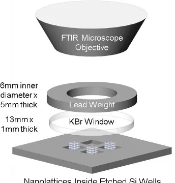
13 Figure 6. Schematic of the nanolattice compression cell setup.
2.4.1. Compression Cell Fabrication
Polished silicon substrates were initially washed with acetone and isopropanol before additional oxygen plasma cleaning. The 1cm x 1cm silicon chips were then spin coated using Shipley 1813 positive photoresist at 3000 rpm for 30 seconds. Samples were soft baked at 115°C for 1 minute. Samples were then exposed to UV light for 15 seconds through a transparency mask containing a 2 x 4 grid of square boxes, each 200μm x 200μm, and spaced 400μm apart. Following UV exposure, samples were developed for 1 min, rinsed with water, and dried under nitrogen. An Oxford Plasmalab System 100 ICP-RIE was used to dry etch wells into the silicon substrate. The dry reactive ion etch (DRIE) process used was a standard Bosch procedure, where the number of cycles was varied between silicon chips to achieve wells with depths ranging from 10-20μm.
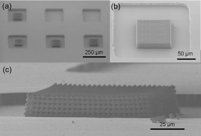
14 file format specific to the Photonic Professional system. On each silicon chip, at least two wells were always left empty so they could be used for taking FTIR background spectra. Following the fabrication and development of the nanolattices, samples were SEM imaged to ascertain the starting height of unstrained structures, and several representative micrographs of the lattices and wells are shown in Figure 7(a-c).
Figure 7. Scanning electron microscopy (SEM) images of representative compression cell samples. (a) A grid of
etched wells with nanolattices fabricated into select wells. Two wells are left empty so they can be used for collecting background FTIR spectra. Image was taken at a 45° tilt. (b) A close-up of a single lattice fabricated within an etched silicon well. Image was taken at a 45° tilt. (c) A close-up of a nanolattice inside a well. Image was taken at a 92° tilt, so that it is possible to see that the nanolattice extends beyond the edge of the well (which is important for subsequent compression).
Polished potassium bromide (KBr) slides were then carefully placed on top of the grid of etched silicon wells and nanolattices, in the next step of creating the compression cell. These circular slides were purchased from International Crystal Labs, and had the following dimensions: 13mm diameter, and 1mm thickness.
15
2.5. Results and Discussion of Band Gap Tuning using Mechanical Strain
Using the compression cell described above, it was possible to strain an as-fabricated sample to a preordained position, and fix it in the strained state by bounding from above by the IR-transparent KBr slide, while it sits affixed to the polished Si substrate. We then collected reflectance with the same FT-IR spectrometer as used on the effectively strained samples. Four experiments on cyclically strained nanolattices were carried out, with each one corroborating the finding that compressing an octahedron nanolattice leads to a blueshifting in the PhC stopband, and releasing the load shifts the stopband back to within 89.8 ± 2.8% of the original stopband position of the pristine nanolattice—a value commensurate with the ~90% recovery observed in nanolattice height following primary compression. Figure 8 shows the reflection spectrum of a representative sample. For this particular sample, the stopband of the initial nanolattice was centered at 7.32μm and that of the 15.2% strained nanolattice blueshifted to 6.34μm.
Figure 8. Normalized reflectance spectra for an as-fabricated nanolattice outside of the compression cell (red), and under compression (blue) using the custom FTIR compression cell setup.
16 light that has been reflected internally between the parallel surfaces35. The number and the position of interference fringes allow us to estimate the pathlength through the compression cell35, which is equivalent to the thickness of the sample and the height of the compressed nanolattices:
𝒅 = 𝑵𝝀𝟏𝝀𝟐
𝟐𝒏𝒆𝒇𝒇𝐜𝐨𝐬 𝜽(𝝀𝟐−𝝀𝟏) (4)
Here, d is the sample thickness or compression cell pathlength, N is the number of interference fringes between the wavelength range λ1 and λ2, neff is the effective refractive index of the material within a well of
the compression cell, and θ is the average angle of incident light on the sample. Having measured the height of pristine, unstrained nanolattices using SEM imaging, and calculated the cell pathlength for a compressed sample, we obtained a value for applied compressive strain. Full details on this analysis are provided in the subsequent section.
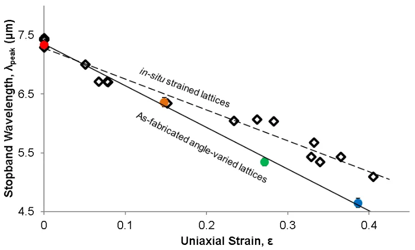
Figure 9. Strain-stopband plots comparing data from the as-fabricated angle-varied lattices under corresponding effective strain, and experimentally strained nanolattices using a compression cell over multiple cycles.
[image:28.612.100.506.344.589.2]17 nanolattices, also plotted in Figure 8 for comparison. This plot reveals that nanolattices strained by 40.5% exhibited a stopband shift of 2.19μm, compared to a 2.87μm shift for the effectively strained angle-varied nanolattices compressed by the same amount. This plot also shows that at high strains of ε ~ 40%, the percent error between the measured λpeak for in-situ strained and angle-varied lattices is 14.1%, while at low strains, on the order of ε ~ 10%, the percent error is significantly smaller, at 1.7%. These deviations likely arise from minor shearing in the in-situ setup that accompanies the nominal uniaxial compressive straining of the lattice. Shear strain in this system may take the form of a torqueing at the nodes of the unit cells comprising the lattice, which leads to a shape change rather than a volume change, and does not affect the periodicity of the lattice in the vertical direction to the same degree predicted by the angle-varied lattices modelling effective strain. It has been previously shown that the stopband position increases nonlinearly with shear strain4, which may also contribute to our observation of larger deviations from the λ
peak position of the angle-varied lattices modelling effective strain, where only uniaxial strain was taken into account.
2.5.1. Calculating Compression Cell Pathlength Using the Interference Fringe Method
Interference fringes in an FTIR spectrum can be a convenient method for determining the lattice thickness or cell pathlength. Per reference 35, pathlength of the cell may be calculated as
𝒅 = 𝑵
𝟐𝒏𝒆𝒇𝒇(𝝂̅̅̅−𝝂𝟏 ̅̅̅)𝟐 (5)
where d is pathlength, N is the number of interference fringes between wavenumbers 𝜈̅1 and 𝜈̅̅̅2, and neff is
the effective refractive index of the material between the two surfaces generating the interference fringes. As described previously, the Nicolet Continuum Infrared Microscope FTIR spectrometer used in our experiments illuminates the sample in an annulus with an angular range between 16°-35.5° relative to the normal. This non-normal incidence necessitates the addition of a cosine term to equation (5) for more accurate calculations of cell pathlength:
𝒅 = 𝑵
18 where θ is the average angle of incident light on the sample. For all our calculations of the cell pathlength d, we used an average angle of 25.75° to the normal.
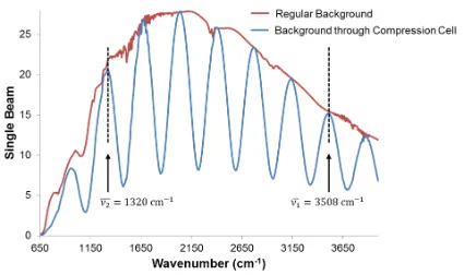
Figure 10. FTIR spectra of a background collected against a regular polished silicon surface, and a background collected against the bottom of an empty etched silicon well through a KBr window, as part of the compression
cell. Interference fringes appear in the compression cell spectrum due to reflection between the internal faces of the
polished KBr window and Si surface at the bottom of the well.
19 fringes between wavenumbers ̅̅̅𝝂𝟏 and 𝝂̅̅̅𝟐. Per Figure 10, ̅̅̅𝝂𝟏= 3508 cm-1, 𝝂̅̅̅𝟐= 1320 cm-1, N = 6, θ = 25.75°,
and neff = 1 (we take this measurement against the silicon surface of an empty well, so the effective medium
is just air). For the specific compression cell background spectrum in Figure 10, cell pathlength/sample thickness (a measure of the distance between the bottom of the polished KBr slide and the silicon surface of the etched well) is d = 15.2μm. It is by this process that we calculated heights for compressed nanolattices residing in neighboring wells on the same silicon chip. The fringes found in background spectra were often clearer than the fringes which manifested in the reflection spectra of actual compressed nanolattices (see Figure 8)—fringes in compressed nanolattice spectra may become convolved with other features of the reflection spectra—and as such background spectra were used preferentially for cell pathlength calculations.
2.6. Comparison of Experimental Bandgap Position and Simulated Bandgap Results
20 Figure 11. Results of simulated reflectance for effectively strained nanolattices compared to experimental data.
(a) Normalized reflection spectra under normal illumination for a simulated 45° unstrained octahedron nanolattice, and three simulated angle-varied nanolattices, each with corresponding degrees of increasing effective strain. The main peak for each simulated nanolattice corresponds to a 1st order Bragg reflection; secondary peaks that appear at
longer wavelengths are caused by the higher order Bragg reflections. (b) Strain-stopband plots comparing data from the as-fabricated angle-varied lattices under corresponding effective strain, experimentally strained nanolattices using a compression cell over multiple cycles, and the simulated angle-varied lattices at normal incidence, and 25.7° incidence.
Figure 11(a) shows the reflectance spectra for four different simulated angle-varied octahedron unit cells, 45°, 40°, 35°, and 30°, illuminated with a normal-incidence plane wave. The simulations show a clear blueshift of the reflection peak with decreasing apex angle of the octahedron unit cell, in agreement with experimental results.
21 in the fabricated samples, like the imperfect uniformity of beams and unit cells and buckling at the joints between unit cells.
The reflection peak observed in our experiments and simulations can be attributed to the 1st order Bragg reflection in the lattice. Bragg’s law is formulated as 2𝑑 × 𝑐𝑜𝑠𝜃 = 𝑛𝜆, where d is the vertical separation
between two layers in the lattice, θ is the angle of the incident beam with the normal line, and n is the order of the Bragg reflection. A monotonic decrease in d from uniaxial strain will result in a monotonic decrease in the resonance wavelength 𝜆𝑝𝑒𝑎𝑘. This result is in agreement with the general blueshift trend observed
both in the numerical and experimental data. Additional reflection peaks observed at longer wavelengths can be attributed to higher orders of the Bragg grating, and are substantially weaker than the main peak of the lattice.
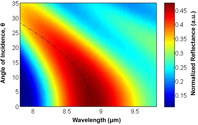
22 Figure 12. A color map depicting the variation in reflection as a function of incident angle and wavelength for
a simulated 45° nanolattice. Note that the angle of incidence here is measured with respect to the line normal to the
surface. At larger angles of incidence, the peak in reflection shifts to shorter wavelengths, and the black dashed line overlaying the data shows the relation between the incident angle and the resonant wavelength given by the Bragg condition equation.
2.7. Conclusions and Evolved Critiques
This work demonstrates fabrication and characterization methodologies for 3-dimensional polymer nanolattices, active in the mid-IR range, whose photonic bandgap can be reversibly modulated as a function of uniaxial compressive strain. Opto-mechanical experiments and theory reveal that applied uniaxial compressive strain and the photonic stopband are linearly related, with a maximum attained bandgap shift of ~2.2μm at ~40% compressive strain. These findings imply that architected nanolattices may be utilized for emerging applications including but not limited to optical strain gauges, accelerometer and other mechanical sensors, as well as tunable laser sources and variable filters. And while 3D lattice fabrication using TPL DLW is currently constrained by the minimum axial resolution attainable, restricting the dimensions of the octahedron geometry studied here to unit cell sizes of no less than 2.5μm, advances like stimulated-emission-depletion (STED) DLW are pushing the resolution limits of this technology, and may soon enable the patterning of any arbitrary 3D lattice with photonic properties extended into the visible
23
Chapter 3: Exploring the Photonic Band Gap Properties of 3D Periodic
Architectures –
Band Gap Properties as a Function of 3D Periodic Architecture
3.1. Outline and Motivation
One of the primary methods for assessing the performance of a PhC is by measuring the quality of its photonic band gap. In general, 3D periodic structures display more complicated bandgap properties than their 2D counterparts and possess more flexibility in applications where the existence of partial stop gaps and a strong suppression rate of some wavelengths are important. Therefore, 3D photonic structures made of low refractive index materials such as polymers can be quite useful in photonic applications. In general, the existence and characteristics of photonic bandgaps depend on such factors as the dielectric contrast and volume fractions, as well as the symmetry, connectivity, and geometrical shape of the periodic dielectric structure.
In this chapter, we report on the optical properties 3D polymeric photonic crystals whose photonic response is dictated by periodic architecture, or more specifically, lattice symmetry. It is noted that local, directional, or “pseudo” band gaps can be easily tuned and even created by changing the size of unit cells comprising the structure. Also discussed is the degree to which finite lattices capture and display the properties predicted by infinite structures and their calculated band structure diagrams.
We study the photonic properties, namely the emergence of pseudo-bandgaps in three different 3D lattice architectures that have been traditionally explored in the context of their mechanical properties. These architectures include octahedron, octet, and tetrakaidecahedron 3D periodic structures, where the octahedron lattice has an underlying simple cubic (SC) structure, the octet lattice has an underlying face centered cubic (FCC) structure, and the tetrakaidecahedron lattice has an underlying base centered cubic (BCC) structure.
3.2. Introduction to Periodic Lattice Architectures
3.2.1. Simple Cubic, Face Centered Cubic, and Base Centered Cubic 3D PhCs
24 simple cubic lattice and found that, despite the appearance of directional stopbands, no complete bandgaps will occur for this architecture, regardless of the volume fraction of spheres. By inverting the dielectric structure however, and placing air spheres in a dielectric background, they obtained the first full photonic bandgap structure with simple cubic symmetry.
Compared to simple cubic PhCs, face centered cubic structures have been very extensively studied, thanks in part to the ease of fabricating opal and inverse opal structures using self-assembly methods. Opals are formed through the close packing of dielectric spheres which results in a natural fcc lattice, and in-filling the air voids in an opal structure with a dielectric and removing the original sphere material, converting it to air, forms the fcc inverse opal structure. The majority of research on FCC 3D PhCs has focused on opal, inverse opal, and woodpile architectures as the former are amenable to fabrication through self-assembly methods, and the latter can be fabricated using conventional lithographic methods.
The study of photonic band gap properties in base centered cubic PhC structures has been somewhat less extensive compared to its sc and fcc counterparts. However, the band gap properties of void-based bcc PhCs in a solidified transparent polymer have been studied,37 as have BCC-based gyroid structures, which have been demonstrated to have a complete gap almost as wide as that of diamond.38
3.2.2. Octahedron, Octet, and Tetrakaidecahedron Lattice Architectures
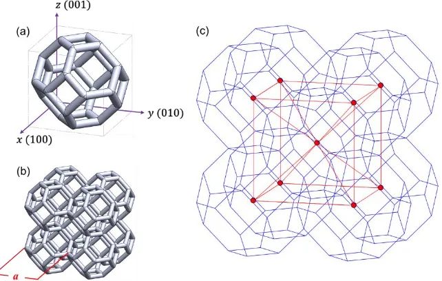
25 Schematics of the octahedron unit cell, lattice, and underlying simple cubic symmetry are shown in Figure13(a-c). It should be noted that lattices are constructed along Cartesian coordinates with the PhC surface pointing along the (001) direction.
Figure 13. Schematic of an octahedron simple cubic PhC lattice. (a) A view the octahedron unit cell with
cylindrical beams. (b) A representation of a 2x2x2 octahedron unit cell lattice. The lattice period is given by the parameter a. (c) Representation of the underlying simple cubic lattice symmetry in the octahedron-based PhC architecture.
26
Figure 14. Schematic of an octet face centered cubic PhC lattice. (a) A view the octet unit cell with cylindrical
beams. (b) A representation of a 2x2x2 octet lattice. The lattice period is given by the parameter a. (c) Representation of the underlying FCC symmetry in the octet-based PhC architecture.
Finally, schematics of the tetrakaidecahedron unit cell, lattice, and underlying base centered cubic symmetry are shown in Figure15(a-c). It should again be noted that lattices are constructed along Cartesian coordinates with the PhC surface pointing in the (001) direction.
Figure 15. Schematic of a tetrakaidecahedron base centered cubic PhC lattice. (a) A view the tetrakaidecahedron
[image:38.612.148.469.434.638.2]27
3.3.Fabrication of 3D Nanolattices PhCs
As described in detail previously, nanolattice PhCs were fabricated out of the acrylate-based “IP-Dip” photosensitive monomer, using the direct laser writing two-photon lithography (DLW TPL) system developed by Nanoscribe GmbH. For this DLW TPL process, the 3D periodic octahedron, octet, and tetrakaidecahedron architectures were created using MATLAB and the computer aided design (CAD) program SolidWorks, with lattice beams defined in slices, so that writing could be performed in a layer-by-layer fashion.39 The layer-by-layer writing scheme allows for the generation of beams possessing nearly circular cross-sections (see ref. 39 for additional detail) , as compared to the octahedron lattices described in Chapter 2 which had elliptical beams. PhC samples were written on a 500μm thick silicon chip, and following the photoresist exposure step, 3D polymer structures were developed for 30 minutes in propylene glycol mono-methyl ether acetate (PGMEA) followed by a 5-minute rinse in isopropyl alcohol. To prevent lattice collapse or excessive shrinkage due to capillary forces during the drying step, lattices were critical point dried using a TousimisAutosamdri-815B, Series B critical point dryer.
28
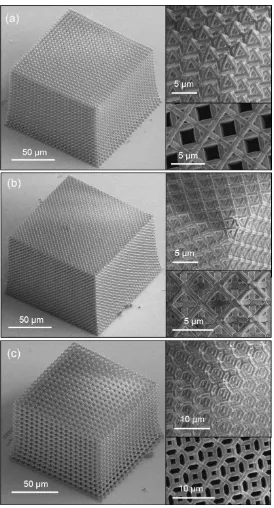
Figure 16. Representative images of as-fabricated octahedron, octet, and tetrakaidecahedron PhC lattices. (a)
Full scale octahedron nanolattice with periodicity a = 4.75µm. Insets show an enlarged lattice corner and round, cylindrical beams, and a top down view of the simple cubic octahedron arrangement. (b) Full scale octet nanolattice with periodicity a = 4.75µm. Insets show an enlarged lattice corner and round, cylindrical beams, and a top down view of the face centered cubic octet arrangement. (c) Full scale tetrakaidecahedron nanolattice with periodicity a = 6.75µm. Insets show an enlarged lattice corner and round, cylindrical beams, and a top down view of the base centered cubic tetrakaidecahedron arrangement.
29 periodic arrangements will typically be close packed, resulting in FCC PhCs with a (111) crystal surface arrangement, as is the case with opal structures.
3.4. Optical characterization of Octahedron, Octet, and Tetrakaidecahedron Nanolattices PhCs
Reflection spectroscopy is a customary optical characterization technique which reveals stop bands as peaks of increased reflection, indicating the nonzero imaginary component of the wavevector for those frequencies contained in the stop band. While all lattices under study are purely polymeric, possessing a relatively low dielectric contrast with air compared to a high-index material like silicon (the refractive index of IP-Dip is n = 1.49 in the mid-IR), we nonetheless expect at least a directional stopband to be present in these PhC structures.
The micron-scale unit cell sizes of our lattices suggest that the PhCs will exhibit a bandgap in the infrared range. As such, we used Fourier Transform Infrared (FTIR) microspectroscopy in reflectance mode to measure stopband position. Spectra were acquired on a Nicolet iS50 FT-IR spectrometer equipped with a Nicolet Continuum Infrared Microscope. The microspectrometer Cassegrain lenses limited incident light to an off-normal annulus with an angular range between 16°-35.5°. All spectra were collected against a smooth, fully reflective gold mirror background.
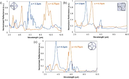
3.4.1. Reflectivity Spectra with respect to Geometry and Periodicity
In Figure17(a) we have two representative reflectivity spectra plotted for simple cubic PhC lattices of octahedron unit cells with periodicities equal to 3.3µm and 4.75µm. For the lattice with average periodicity of 3.3µm, a significant peak in normalized reflectance emerges, and is centered at 6.41μm, which corresponds to the first order stopband. For the lattice with an average period of 4.75µm, the first order stopband appears at 9.69μm.
30 peaks at 4.89μm 3.20μm, and these positions are consistent with 2nd and 3rd order Bragg reflections respectively.
It should also be noted that most of the sharp, intense dips we observe in our nanolattice PhC spectra are not optical features belonging to the nanolattice architecture, but are instead absorptions from the polymer material. Some of these material absorptions pass through the relevant stopband features of the lattice, like the dips at 9.39μm and 10.13μm in the 4.75µm octahedron lattice, but these are actually caused by excited vibrational modes of the IP-Dip polymer (see Appendix A for more detail).40
Figure 17. FTIR reflectance spectra for octahedron, octet, and tetrakaidecahedron nanolattice PhCs. (a)
Normalized reflectance spectra for octahedron nanolattice PhCs with 3.3µm and 4.75µm periodicities. (b) Normalized reflectance spectra for octet nanolattice PhCs with 3.5µm and 4.75µm periodicities. (c) Normalized reflectance spectra for tetrakaidecahedron nanolattice PhCs with 4.3µm and 6.75µm periodicities.
[image:42.612.85.536.264.540.2]31 that stopband position is dependent on lattice period, with a decreasing unit cell size leading to blueshifting of the stopband peak.
Finally, in Figure17(c) we have two representative reflectivity spectra plotted for base centered cubic PhC lattices of tetrakaidecahedron unit cells with average periodicities equal to 4.3µm and 6.75µm. For the lattice with a = 4.3µm, a significant peak in normalized reflectance emerges at 4.16μm, which corresponds to a stopband. For the lattice with a = 6.75µm, a stopband appears at 6.34μm. These results again corroborate that, regardless of lattice architecture, stopband position is highly influenced by lattice period, and by decreasing the unit cell size of any architecture with any underlying lattice symmetry, the center position of the stopband will blueshift.
3.5. Comparing Experimental Reflectivity to Calculated Photonic Band Structure
3.5.1. Photonic Band Structure CalculationsIn order to carry out a comparison of our experimental results with theory, we have calculated the photonic band structures associated with our three unique cubic PhC systems using the plane wave expansion (PWE) method.41 In PWE, Maxwell’s equations are combined to obtain the differential wave equation that governs the propagation of the electromagnetic waves within a PhC structure, and assumes an infinite, ideal photonic crystal. Photonic band structures for octahedron, octet, and tetrakaidecahedron architectures were simulated and analyzed using the commercially available BandSOLVE simulation engine, which utilizes an optimized implementation of the PWE technique for periodic structures.
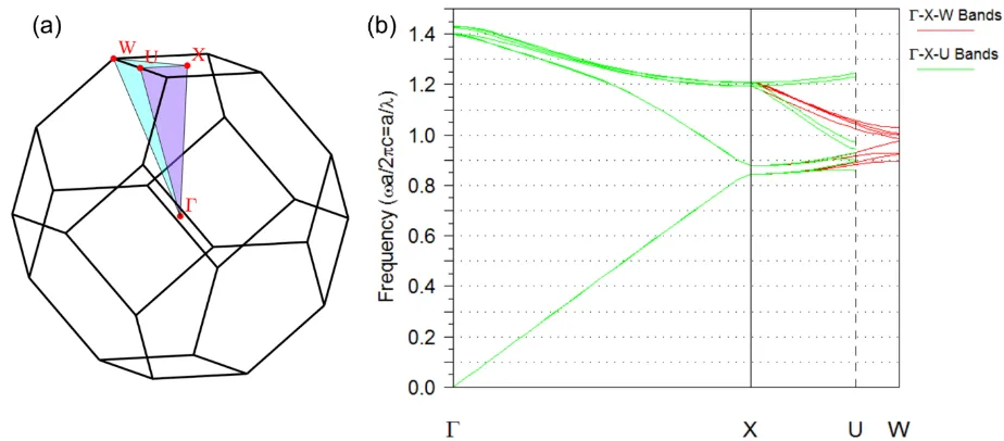
To construct the photonic bands, we take wave vectors from the edges of the underlying lattice symmetry irreducible Brillouin zones (as commonly done in the photonic literature42), where particular points along the Brillouin zone path correspond to different magnitudes and directions of the wave-vector
k⃗. For each chosen k⃗ path, the corresponding eigenvalues are calculated, forming an ascending set
of n eigenvalues. In grouping the eigenvalues and plotting them as a function of k⃗, band diagrams are
32 Consequently, we expect that with a small polymer index of n = 1.49, the widths of our bandgaps for all lattice symmetries will be rather small.
Figure 18. Brillouin zone and band structure calculated for the octahedron simple cubic lattice. (a) The Brillouin
zone for a simple cubic PhC set relative to the wave vectors incident on the simple cubic octahedron lattice during FTIR reflectance measurements. The angular range of the incident light annulus means wave vectors will interface with the Γ-X-R and Γ-X-M planes (denoted in blue and pink). (b) Band structure calculated for the octahedron simple cubic lattice probing the Γ-X-R and Γ-X-M directions. Bands are compared for lattices with a periodicity of 4µm and 5µm.
33 width diminishes and moves to higher frequencies the further we move in X-R and X-M. It is likely that the peaks we observe in our FTIR reflectance spectra are due to this propagating bandgap in the X-R and X-M directions. We also note that, while the overall band structure shape is identical for octahedron lattices with 4µm and 5µm periodicities, band and bandgap positions are all shifted to higher frequencies (longer wavelengths) as periodicity increases. This is likely because the beam diameter used in both simulations is set to 850nm, meaning that the 5µm lattice possesses a slightly lower fill fraction compared to the 4µm lattice.
Figure 19. Brillouin zone and band structure calculated for the octet face centered cubic lattice. (a) The Brillouin
zone for a face centered cubic PhC. The Γ-X-U and Γ-X-W planes (denoted in purple and light blue) are singled out as the planes which coincide with wave vectors of light incident on the octet PhC from FTIR reflectance measurements. (b) Band structure calculated for the octet FCC lattice along the Γ-X-U and Γ-X-W directions. Bands along the X-U and X-W directions are overlaid to show their similarities.
34 opens between bands 2 and 3 at the Γ-X edge, and this bandgap continues to propagate in both the X-U and X-W directions, though the bandgap width diminishes and moves to higher frequencies the further we move along these k-paths. The peaks we observed in our FTIR reflectance spectra for octet PhC samples are likely due to the bandgap which appears in both the X-U and X-W directions.
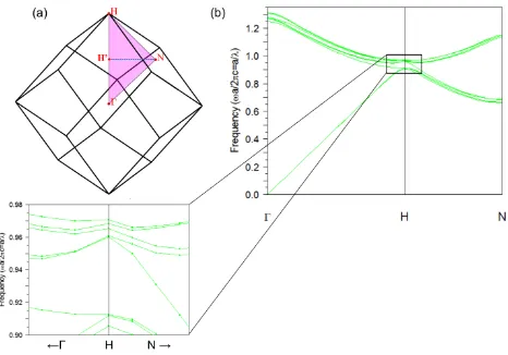
Figure 20.Brillouin zone and band structure calculated for the tetrakaidecahedron base centered cubic lattice.
(a) The Brillouin zone for a base centered cubic PhC. The Γ-H-N plane (denoted in pink) is singled out as the plane which coincides with wave vectors of light incident on the tetrakaidecahedron PhC from FTIR reflectance measurements. (b) Band structure calculated for the tetrakaidecahedron BCC lattice along the Γ-H-N direction. Inset shows an expanded view of bands and band gaps around the H point.
35 tetrakaidecahedron base centered cubic PhCs along the Γ-H-N path, and observe a small bandgap opening between bands 6 and 7 at the Γ-H edge (see the expanded band plot in Figure 20(b)). This bandgap continues to propagate along the H-N direction, shifting to higher frequencies while the bandgap width increases, and then contracts the further we move along this k-path. The peaks we observed in our FTIR reflectance spectra for tetrakaidecahedron PhC samples are likely due to the appearance of this bandgap in the H-N direction.
3.5.2. Direct Comparison of Peak Reflectivity and Bandgap Position
36 Figure 21. Calculated bands and experimental reflectivity peaks for simple cubic octahedron nanolattice PhCs.
(a) Calculated bands (green lines) along the X-M direction and experimental reflectivity peaks (grey and black lines) for octahedron lattices with 3.3µm periodicity. (b) Calculated bands (green lines) along the X-R direction and experimental reflectivity peaks (grey and black lines) for octahedron lattices with 3.3µm periodicity. (c) Calculated bands (green lines) along the X-M direction and experimental reflectivity peaks (light grey, dark grey, and black lines) for octahedron lattices with 4.75µm periodicity. (d) Calculated bands (green lines) along the X-R direction and experimental reflectivity peaks (light grey, dark grey, and black lines) for octahedron lattices with 4.75µm periodicity.
37 attribute deviations in reflectivity peak position to inhomogeneities in unit cell size throughout the PhC height. During lattice fabrication, some measure of lattice shrinkage is inevitable, resulting in the unit cells affixed to the substrate being larger than unit cells near the lattice top, meaning peak reflectivity is actually a convolution of the stopband positions of PhCs with multiple periodicities.
[image:49.612.83.541.355.681.2]In Figure 21(c-d) we plot the center peak position of experimentally measured stopbands for three octahedron lattice samples (light grey, dark grey, and black lines) with an approximate unit cell size of 4.75µm, relative to the bands for an ideal 4.75µm octahedron PhC. We observe that in both the X-M and X-R directions, experimental reflectivity peaks noticeably overlap the bandgap region, and that is overlap is more substantial relative to the plots in Figure 21(a-b) for the 3.3µm octahedron PhCs. One reason for this is that the 4.75µm samples are more homogeneous throughout their height, and as such, better approximate an ideal simple cubic octahedron lattice with constant periodicity.
Figure 22. Calculated bands and experimental reflectivity peaks for face centered cubic octet nanolattice PhCs.
38
for octet lattices with 3.5µm periodicity. (b) Calculated bands (green lines) along the X-U direction and experimental reflectivity peaks (grey and black lines) for octet lattices with 3.5µm periodicity. (c) Calculated bands (green lines) along the X-W direction and experimental reflectivity peaks (light grey, dark grey, and black lines) for octet lattices with 4.75µm periodicity. (d) Calculated bands (green lines) along the X-U direction and experimental reflectivity peaks (light grey, dark grey, and black lines) for octet lattices with 4.75µm periodicity.
In Figure 22(a-b) we plot the center peak position of experimentally measured stopbands for two octet lattice samples (grey and black lines) with an approximate unit cell size of 3.5µm, relative to the bands for an ideal 3.5µm octet PhC. we observe that in both the X-W and X-U directions, experimental reflectivity peaks overlap the bandgap region, but are far from centered over the gap at their respective frequencies. This is likely caused by significant inhomogeneities in periodicity throughout the PhC volume. It should be noted that the X-U k-path is shorter than the X-W k-path, and consequently FTIR reflectance measurements actually sample regions of the 2nd FCC Brillouin zone (not shown here) as well as the 1st Brillouin zone.
Figure 22(c-d) presents the experimental reflectivity peaks for three octet PhC lattices (light grey, dark grey, and black lines) with a periodicity of 4.75µm plotted with the band structure of an ideal 4.75µm octet PhC. Similar to what we observe in Figure 22(a-b), experimental measurements overlap with the bandgap at the respective center frequencies for the reflectivity peaks. However, all of our experimentally measured octet samples present larger deviations in k-path position compared to our experimentally measured octahedron samples, and the reasons for this observation must be explored in a subsequent study.
Figure 23. Calculated bands and experimental reflectivity peaks for base centered cubic tetrakaidecahedron
nanolattice PhCs. (a) Calculated bands (green lines) along the H-N direction and experimental reflectivity peaks
39 In Figure 23(a) we plot the center peak position of an experimentally measured stopbands for a tetrakaidecahedron lattice sample (black line) with an approximate unit cell size of 4.3µm, relative to the bands for an ideal 4.3µm tetrakaidecahedron PhC. We observe that the experimental reflectivity peak overlaps the bandgap region in its entirety, unlike the behavior observed in octahedron and octet lattices. In Figure 23(b) we plot the center peak position of an experimentally measured stopbands for a tetrakaidecahedron lattice sample (black line) with an approximate unit cell size of 6.75µm, relative to the bands for an ideal 6.75µm tetrakaidecahedron PhC. We again observe that the experimental reflectivity peak overlaps the bandgap region in its entirety. However, for both periodicities, the experimental reflectivity is not centered over the band gap region for each individual center frequency. An implication of this is that non-idealities likely exist in the tetrakaidecahedron nanolattices, but the angular window for FTIR measurements is wide enough that the likelihood of hitting the correct k-vectors which coincide with the band gap region is substantially large.
3.5.3. Comparing the FWHM of Reflectivity Peaks to Calculated Bandgap Width
40 will become less intense and asymmetric, and may become spectrally wider due to lattice defects and disorder.44
Figure 24. Outline for comparing the FWHM of experimental reflectivity peaks to the calculated bandgap
width Δω. (a) Experimental reflectivity peaks are fit to a Gaussian curve and the full width at half maximum is
measured around the center peak frequency ωo. (b) At the same center frequency we measure the bandgap width, Δω,
from the PhC band structure diagrams.
Another manner by which we can assess the quality of reflection peaks, namely how well they correspond to the expected bandgap properties, is by comparing the full width at half maximum (FWHM) of the experimental peaks, to the corresponding calculated bandgap width Δω, at the relevant center gap
frequency. This process is outlined in Figure 24(a-b). We take the experimentally obtaine