Abstract—With the development of the Internet of Things
(IoT), various signal processing algorithms have been widely used in IoT devices. Convolutional neural networks (CNN), image processing algorithms and speech processing algorithms are important signal processing algorithms that play an important role in various intelligent IoT devices. In order to enable IoT devices with limited computing power to support various signal processing algorithms, In this paper, we propose a small area reconfigurable multi-algorithm accelerator to accelerate various signal processing algorithms through hardware. The accelerator realizes reconfiguration of its own structure based on Dynamic Partial Reconfiguration (DPR) function of FPGA. A SoC verification system based on Cortex-M3 is constructed to verify the performance of the designed accelerator. The Lenet-5 network, Sobel Edge Detector algorithm and FIR filtering algorithm are implemented on this accelerator. The execution time of Lenet-5 network is compared with that of Intel i5 7500, Cortex-A53 and Cortex-A7 CPU. The execution time of Sobel Edge Detector algorithm and FIR filtering algorithm is compared with software implementation of same design on Cortex-M3 core. The comparison results show that the CNN computing power of the proposed accelerator exceeds that of Cortex-A53 and Cortex-A7 at the main frequency of 50MHz. The computing time of Sobel Edge Detector algorithm and FIR filter algorithm is also reduced in comparison to the software implementation.
Index Terms—Multi-Algorithm Accelerator, FPGA, CNN,
IoT
I. INTRODUCTION
ITH the development of convolution neural network, mobile edge computing and the wide application of multimedia sensors in IoT system, the IoT system is developing in the direction of diversification of application scenarios, high quality of service requirements and popularization of participating objects [1]. The popularity of multimedia sensors such as voice and image, as well as the development of artificial intelligence algorithms from the
Manuscript received July 17, 2019. This work was supported by the National Natural Science Foundation of China (No. 61774086), the Fundamental Research Funds for Central Universities (No. NP2019102, NS2017023), and the Natural Science Foundation of Jiangsu Province (No.BK20160806).
L. Zhang is with College of Electronic and Information Engineering, Nanjing University of Aeronautics and Astronautics, Nanjing, 211100, China (e-mail: [email protected]).
N. Wu is with the College of Electronic and Information Engineering, Nanjing University of Aeronautics and Astronautics, Nanjing, 211100, China (e-mail: [email protected]).
F. Ge, Muhammad Rehan Yahya and F. Zhou are with the College of Electronic and Information Engineering, Nanjing University of Aeronautics and Astronautics, Nanjing, 211100, China
cloud to the end, pose new challenges to the complex signal processing ability of IoT processors [2]. The traditional DSP is mainly oriented to high-speed radar signal or communication signal processing algorithms. It has high cost, large power consumption and unsatisfactory acceleration performance of artificial intelligence algorithms such as convolutional neural networks [3]. Therefore, it is not suitable for wide application in IoT node devices. The special processor chips for accelerating artificial intelligence algorithms, such as TPU and GPU, have achieved high computing throughput, but they are expensive and high power consumption. They are generally used in cloud computing [4-5], and are not suitable for the Internet of Things system. Therefore, it has become a research hotspot in the field of integrated circuit design to develop new signal processing accelerators for the mainstream signal algorithms in the current IoT systems.
With the increasing number and variety of sensors in the IoT system, the corresponding signal processing algorithms are constantly updated. From reference [6-12], it can be concluded that the main signal processing algorithms in IoT system are image processing, speech signal processing, digital filtering and convolution neural network operation. These algorithms are composed of a combination of basic arithmetic units such as multiply and accumulate, matrix convolution, matrix addition, and data extraction. For example, the convolutional neural network algorithm contains convolution, normalization, non-linearity and extraction operations. Similarly, the image processing algorithm is usually composed of image extraction and two-dimensional convolution operations. Through the hardware implementation of common operation components of these signal processing algorithms, and combining the computing components according to the needs of the actual algorithm, the acceleration of various signal processing algorithms is realized. As a product between general-purpose chip and special-purpose chip, FPGA not only provides higher operating efficiency and lower power consumption, but also has the characteristics of flexible configuration. DPR technology enables FPGA devices to implement highly complex circuit functions under limited hardware resources, while performing software and hardware tasks at high speeds, it significantly reduces the system cost and power requirements [13].
In this paper, a reconfigurable small area multi-algorithm accelerator for signal processing applications is proposed and designed based on the consideration of circuit area and acceleration performance. Firstly, the basic arithmetic unit is extracted from the mainstream IoT signal processing
DPR based Small Area Reconfigurable
Multi-Algorithm Accelerator for IoT System
Lei Zhang, Ning Wu, Fen Ge, Muhammad Rehan Yahya and Fang Zhou
algorithms such as neural network algorithm, image processing and speech signal processing, and four reconfigurable computation acceleration chains are designed. Then, the basic acceleration unit is specially combined by the DPR technology of FPGA to realize hardware acceleration of convolution neural network, image processing and speech signal processing.
The rest of the article is organized as follows. Section II introduces the overall design of the accelerator and the specific design of the basic acceleration unit. In Section III, the accelerator verification system, including SoC based on Cortex-M3, implementation of Lenet-5 network, Sobel edge detection algorithm and FIR filter implementation is discussed. Section IV demonstrates the acceleration performance and resource consumption of the accelerator. Finally, the conclusion and future work is furnished in Section V.
II. ACCELERATOR DESIGN A. Accelerator Structure
In this paper, the designed multi-algorithm accelerator is different from the performance-seeking accelerator. Considering that the IoT system has the characteristics of limited power consumption and diverse application scenarios, the designed accelerator needs to take into account the resource consumption and versatility of the circuit while improving its performance. The accelerator is mainly composed of four reconfigurable computation acceleration chains, whose structure is shown in Fig. 1.
acceleration chain1 acceleration chain2 acceleration chain3 acceleration chain4 ram
mux
32b
32b
32b
32b
4×32b 4×32b
block ram1
coe ram src data
read
Src A
Src B
Src C
Src A
Src B
Src C
Src A
Src B
Src C
Src A
Src B
Src C
Result
Result
Result
Result
block ram2
128b
128b
M
UX
S
oC BU
S
PRC
ICAP
ICAP ICAP ICAP Src A
Src B Src C ICAP
M
UX
M
UX
result
[image:2.595.65.273.424.590.2]RM1 RM2 RM3 RM4
Fig. 1. The architecture of the multi-algorithm accelerator
The accelerator includes a source matrix data loading module(src data read), a convolution kernel buffer module(coe ram), a reconfigurable circuit controller(PRC), two ping-pong buffer blocks(block ram1 and block ram2), and four reconfigurable computation acceleration chains(acceleration chain1 to acceleration chain4). Each reconfigurable computation acceleration chain consists of four Reconfigurable Modules(RM1 to RM4). The four Reconfigurable Modules can be configured with different functions to accelerate the different signal processing algorithms. The entire accelerator is mounted on the system bus via the AHB bus, allowing other components in the SoC to parameterize and access the acceleration unit.
B. Convolutional Circuit Design
Convolution is widely present in various signal processing
algorithms which consumes most of the computation time. In speech signal processing, the conversion of speech signals from time domain to frequency domain and the filtering of speech signals are all based on one-dimensional convolution. In CNN algorithm and image processing algorithm, two-dimensional convolution occupies a large number of operations. In CNN, the two-dimensional matrix convolution operation accounts for more than 90% of the total network computation [14]. Optimization of the convolution operation will significantly improve the resource utilization and computational performance of the signal processing algorithm. A convolution operation of an two-dimensional N*N matrix X and a k*k-sized convolution kernel W can be expressed as:
( -1)/ 2 ( -1)/ 2
, , ,
-( -1)/ 2 -( -1)/ 2
*
k k
n m n i m j i j
i k j k
Y X + + W
= =
= ∑ ∑ (1)
It can be seen from the equation (1) that the amount of data to be loaded by convolving an N*N matrix with a k*k convolution kernel is k*k*(N−k+1)*(N−k+1). The one-dimensional convolution can be regarded as an N*1 matrix convoluted with a k*1 convolution kernel, and the amount of data to be loaded is k*(N−k+1).
Due to the nature of convolution operations, there is a large amount of duplication in the required data, and the loading of duplicate data consumes the bus access bandwidth while limiting the throughput of its own operation, thereby, affecting the performance of the entire system. To reduce the data bandwidth occupation of the convolution operation and improve the throughput rate of the acceleration unit, a low bandwidth occupied convolution operation circuit is designed from the angle of reducing the data overload rate. The structure of the convolution operation circuit is shown in Fig. 2.
Address Generation
Unit Source Data
Loading Unit
Convolution Kernel Data Loading Unit
Multiplier
Accumulator
Src A Src B
Result
Fig. 2. The architecture of the convolution operation circuit
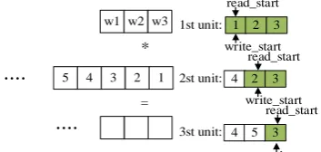
Source data loading unit in the convolution circuit is the key to reduce data bandwidth. Source data loading unit consists of a data reading unit and cyclic queue. For the loading of one-dimensional source data, take a third-order convolution kernel as an example. The loading process of convolution data is shown in Fig. 3.
5 4 3 2 1 1st unit:
2st unit:
3st unit:
....
....
write_start read_start
1 2 3
4 2 3
write_start read_start
4 5 3 read_start
write_start w1 w2 w3
*
[image:2.595.344.506.460.583.2]=
[image:2.595.335.512.683.767.2]When the convolution begins, the source data loading unit loads three data of the first round of convolution operation into the loop queue from memory and points the read_start and write_start pointers of the loop queue to the front end of the queue. The back-level computing unit takes out the three data from the loop queue for operation. After each round of calculation, one data is taken out of the memory and written to one memory unit pointed by the write pointer, and then read_start and write_start loops are moved back by one bit.
For the loading of two-dimensional source data, take the convolution of a 5*5 matrix and a 3*3 convolution kernel as an example. The convolution data loading process is shown in Fig. 4.
When the convolution begins, the read_start and write_start pointers of the loop queue point to the front end of the queue. The source data loading unit will load the nine data in the first round of the convolution operation into the loop queue according to the column priority. The back-level operation unit will take out the nine data needed in the first round of operation from the loop queue. When the first round of operation is completed, the source data loading unit takes three data from memory and writes them into the three memory units pointed by the writing pointer. Then the read_start and write_start loops are moved back three bits. The back-level operation unit reads the nine data needed in the second round from the address pointed by the read_start. The subsequent data loading methods are recursive in turn.
According to the previous analysis, for one-dimensional convolution, an array with N points is convoluted with a convolution core of order k. In theory, the number of data to be loaded is k* (N-k+1), and the optimized amount of data to be loaded is:
( ) 1
k + N - k * = N (2) The optimization rate
η
is:N =
-k* N -k+
η 1
( 1)
(3)
For two-dimensional convolution, a matrix of N*N is convoluted with a convolution core of k*k. In theory, the number of data to be loaded is k*k*(N−k+1)*(N−k+1), while the optimized amount of data to be loaded is:
(k * k + N - k * k * N - k +( ) ) ( 1)= N * k * N - k +( 1) (4) The optimization rate
η
is:N*k* N-k+ =
-k*k* N-k+ * N-k+
η 1 ( 1)
( 1)( 1) (5)
C. Reconfigurable Design
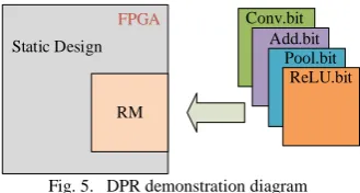
DPR is a FPGA design technology provided by Xilinx to efficiently utilize FPGA resources and realize the reusable use of FPGA resources. On the one hand, it allows reprogramming of the FPGA designated area with new
functionality, on the other hand, it allows the current design to continue running in the remaining space of the device. The DPR demonstration diagram is shown in Fig. 5.
Conv.bit Add.bit
Pool.bit ReLU.bit Static Design
FPGA
[image:3.595.54.466.57.159.2]RM
Fig. 5. DPR demonstration diagram
Conv. bit, Add. bit, Pool. Bit and ReLU. bit are downloaded to Reconfigurable Module (RM) respectively, and the corresponding functions can be implemented in turn.
[image:3.595.345.510.214.302.2]To support more signal processing algorithms, this accelerator realizes the reconfigurable design of computation acceleration chain based on DPR function of FPGA. Each computation acceleration chain of the accelerator is divided into four Reconfigurable Modules. Its structure is shown in Fig. 6.
Src A Src B Src C
result
S o C B U S Applicat
ion
BPI Flash
ICAP configure Triggers
Control
VSM VSM VSM VSM
Fetch Path
PRC
[image:3.595.306.548.427.555.2]RM1 RM2 RM3 RM4
Fig. 6. The reconfigurable design
Through the control of PRC module, each Reconfigurable Module can dynamically load one of the convolution circuits, pooling circuit, matrix addition circuit and activation circuit, thus realizing any combination of these four circuits, so that the input data stream can pass through any one or more computational modules. Therefore, the accelerator can realize the acceleration function of convolution neural network, image processing, speech signal processing and other signal processing algorithms through parameter configuration.
AXI-S bus is used for data transmission between Reconfigurable Modules. AXI-S is an on-chip bus for high-speed data transmission in Advanced Microcontroller Bus Architecture (AMBA) bus cluster. It has the characteristics of simple control logic and high transmission efficiency. The PRC module uses the Partial Reconfiguration Controller IP provided by Xilinx to implement the control logic of the Reconfigurable Modules. Its structure is shown in Fig. 7.
11 12 13 14 15
21 22 23 24 25 16 17 18 19 20
1 2 3 4 5
6 7 8 9 10
w7 w8 w9 w1 w2 w3
w4 w5 w6
*
=
4 9 14 5 10 15 3 8 13
write_start read_start
4 9 14 2 7 12 3 8 13
write_start read_start
1 6 11 2 7 12 3 8 13
write_start read_start
1st unit:
2st unit:
3st unit:
Virtual Socket Manager1
Fetch Path Virtual Socket
Manager2
Virtual Socket Manager3
Virtual Socket Manager4
interface to Reconfigurable Module
interface to ICAP AXI-S status Channel1
AXI-S Control Channel1 Tiggers1 AXI-S status Channel2 AXI-S Control Channel2
AXI-S Control Channel4 AXI-S Control Channel3 Tiggers2
Tiggers3
Tiggers4 AXI-S status Channel3
AXI-S status Channel4
[image:4.595.55.277.53.176.2]Memory Mapped interface to BPI Flash Fig. 7. The architecture of the PRC module
PRC module mainly realizes the following functions: reconfiguration trigger signal monitoring, bitstreams file loading, and Reconfigurable Module status query. Virtual Socket Manager monitors trigger events, and trigger signals can be generated by hardware or software. This accelerator uses software trigger mode. When a trigger event occurs, Virtual Socket Manager maps the trigger signal to a specific Reconfigurable Module and manages the reconfiguration of the Reconfigurable Module. Each Virtual Socket Manager runs independently, so when one Virtual Socket Manager manages the Reconfigurable Module, the other can handle trigger events. Virtual Socket Manager must queue up to access Fetch Path. Fetch Path extracts bitstreams from external BPI Flash and sends them to the Internal Configuration Access Port (ICAP) for reconfiguration of the Reconfigurable Module.
III. VERIFICATION PLATFORM CONSTRUCTION A. Design of Verification Platform Based on Cortex-M3
In order to realize the function verification and performance evaluation of the accelerator, a verification platform is built based on the open source Cortex-M3 core of ARM company. Cortex-M3 is a processor core for IoT system released by ARM company. It achieves a good balance between power consumption and performance. The designed SoC structure is shown in Fig. 8.
ROM RAM
B
ri
dge
SPI Timer UART GPIO
int
er
rupt
AHB
APB
Cortex-M3 Core
[image:4.595.309.544.251.348.2]Multi-algorithm Accelerator
Fig. 8. The architecture of SoC
The designed SoC consists of functional units such as Cortex-M3, on-chip memory, multi-algorithm accelerator unit and UART. The Cortex-M3 acts as a processing core in the SoC for executing applications and completing the configuration and invocation of multi-algorithm accelerator units. The on-chip memory of SoC is divided into instruction memory and data memory, which are respectively used to save the instruction code and the data generated at runtime. The multi-algorithm accelerator unit as the object to be tested, realizes acceleration of various signal processing algorithms under the control of the processor. Peripherals such as UART
and GPIO are used as interactive units of the SoC to indicate to the tester the running state of the program so that the user can evaluate the performance of the multi-algorithm accelerator unit to be tested.
B. Implementation of CNN
To verify the acceleration of the CNN algorithm by the accelerator, the classical Lenet-5 network is used in this paper. Lenet-5 is a convolutional neural network for handwritten character recognition, which is regarded as one of the earliest and most classical convolutional neural networks. With the deepening of CNN research, a series of more efficient and accurate CNN structures have been proposed, but Lenet-5, as a classical network structure, is still widely used in the performance evaluation of CNN acceleration unit. The structure of Lenet-5 network is shown in Fig. 9.
convolutions
subsampleconvolutionssubsampleexpansion full connection Input image
32*32 28*28 14*14 10*10 5*5 400*1 10*1
Fig. 9. The architecture of Lenet-5 network
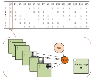
Lenet-5 network consists of five hidden layers: convolution layer C1 with six convolution cores, pooling layer S2, partial connection layer C3 with sixteen convolution cores, pooling layer S4 and full connection layer S6 with ten convolution cores [15]. Convolution layer C1 contains six 5*5 size convolution kernels, and the feature map is activated by ReLU function. Each convolution kernel convolves the original image with an input size of 32*32 to generate six 28*28 feature maps. Partial Connection Layer C3 is the most complex layer in Lenet-5 network. It contains sixteen 5*5 convolution cores. Each convolution core has a partial connection with six feature maps output by S2. After calculation and activation of this layer, sixteen 10*10 feature maps will be obtained. Partial connection relation and calculation process are shown in Fig. 10.
0 1 2 5
4 3
[image:4.595.327.522.546.709.2]feature map 0
Fig. 10.Partial connection relation and calculation process of Layer C3
map of C3 layer is obtained through activation. The pooling layer S4 pools the output of the C3 layer, and the pooling result is sixteen feature maps of 5*5 size. Finally, the expansion layer S5 expands sixteen 5 * 5 feature maps into a 1 * 400 one-dimensional matrix, and the S6 layer connects
TABLEI.THE CALULATION OF EACH LAYER
Layer Calculation formula Explain
C1 0 5 = 0 5
1 1 1 1
[C~C ] relu S[ * [K~K ]] Convolution and ReLU
S2 0 5 = 0 5
2 2 1 1
[S~S ] pool C[ ~C ] Pooling C3
5
0 15 0 15
3 3 2 3 3
0
[ ] [ i*[ ] ]
i
C C relu S K K
=
= ∑
~ ~ Convolution and Matrix
addition and ReLU S4 0 15 = 0 15
4 4 3 3
[S ~S ] pool C[ ~C ] Pooling S5 S5 =[S40~S154] Expansion
S6 0 9 = 0 9
6 6 5 6 6
[S~S ] S * [K ~K ] Full connection
the expanded matrix with ten convolution operators to obtain ten classification results, that is, the recognition results of the input image. Comprehensive analysis of the characteristics of the operation of each layer of the network, the calculation of each layer of Lenet-5 are summarized in Table I as above.
It can be seen from the table above, Lenet-5 network consists of four operations: convolution, matrix addition, activation(ReLU) and pooling. Therefore, these four operations need to be mapped to the four reconfigurable modules of the reconfigurable computation acceleration chain. Considering the flow characteristics of the data flow between the four operations, the four operations are mapped in the order shown in Fig. 11.
Src A Src B Src C
Result
Control
Convolution Matrix
[image:5.595.40.296.128.226.2]addition ReLU Pooling
Fig. 11.Configuration for Lenet-5 Network
The above mapping sequence conforms to the data flow direction between the C1 layer and the S2 layer, and between the C3 layer and the S4 layer. The four operations form a pipeline according to the data flow direction, which can speed up the calculation, reduce data movement, and save power consumption.
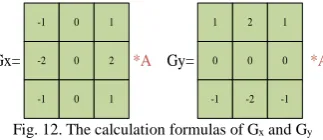
C. Implementation of Sobel Edge Detector and FIR In image processing algorithms, the image edge detection is often needed, and the edge detection based on Sobel operator is a common method. Sobel operator is a first-order gradient algorithm, which has a smooth effect on noise. It is a common method of edge detection when precision requirements are not strict [16]. Sobel operator uses two 3*3 matrix operators to convolute the original image and get the gray values of the horizontal edge and the vertical edge respectively. If A represents the original image, Gx and Gy represent the horizontal edge image and the vertical edge image respectively, the calculation formulas of Gx and Gy can be shown in Fig. 12.
-1 0 1
-2 0 2
-1 0 1
1 2 1
0 0 0
-1 -2 -1
[image:5.595.313.544.187.231.2]Gx= *A Gy= *A
Fig. 12.The calculation formulas of Gx and Gy
The full edge gray value of an image can be approximated
by the following formula:
= +
|G | |Gx | |Gy | (6)
Before image edge detection, it is usually necessary to down sample to reduce the image size and operation data. To sum up, edge detection based on Sobel operator consists of three operations: pooling, convolution and matrix addition. According to the flow characteristics of data flow among the three operations, the three operations are mapped to the reconfigurable computation acceleration chain in the order shown in Fig. 13.
Src A Src B Src C
Result
Control
Pooling Convolution Matrix
addition
[image:5.595.309.539.351.442.2]Pass-through
Fig. 13.Configuration for Sobel Edge Detector
The fourth reconfigurable module is configured as a pass-through without any operation on the data.
In speech signal processing, it is often necessary to filter out the specific frequency in the signal. Due to FIR filter has stability, linear phase, easy to design, easy to achieve on the hardware and other advantages, it has a wide range of applications. In IoT devices, support for FIR filtering has also become a necessary feature. Its serial structure is shown in Fig. 14.
Z-1
Z-1
Z-1
X(n) X(n-1) X(n-N+2) X(n-N+1)
h(0) h(1) h(N-2) h(N-1)
Y(n)
Fig. 14.The serial structure of FIR filter
In the time domain, the output of the FIR filter is the convolution of the input signal with the unit impulse response [17]. the discrete equation can be expressed as:
( ) ( ) * ( ) ( ) ( - ) ( ) ( - )
y n =x n h n =∑x k h n k =∑h k x n k (7)
Where y(n) is the filter output, x(n) is the sample data, and h(n) is the filter coefficient. It can be seen that FIR filters are one-dimensional convolution operations, which only needs to map a convolution operation to the reconfigurable computing acceleration chain, as shown in Fig. 15.
Src A Src B Src C
Result
Control
Convolution
Pass-through Pass-through
Pass-through
Fig. 15.Configuration for FIR filter
The first reconfigurable module is configured as convolution operation, and the other three are pass-through without any operation on data.
IV. PERFORMANCE EVALUATION A. Performance Analysis of Acceleration Unit
To evaluate the performance of the accelerator designed in this paper, the SoC based on the Cortex-m3 kernel described above is used to evaluate the acceleration effect of the accelerator on the three algorithms Lenet-5 network, Sobel Edge Detector and FIR respectively.
[image:5.595.52.286.401.442.2] [image:5.595.310.544.569.620.2] [image:5.595.87.249.698.768.2]high-performance ARM processors are selected as the evaluation and comparison objects of Lenet-5 network acceleration effect by this accelerator. In order to calculate the execution time of Lenet-5 network on different CPUs, the C language Lenet-5 forward propagation program is run on Intel 7500, Cortex-a53 and Cortex-a7 respectively, and is compared with the running time of Lenet-5 in this accelerator. The forward propagation execution time of Lenet-5 on each platform is shown in Table II.
TABLEII.EXECUTION TIME OF LENET-5 ON EACH PLATFORM
CPU Core Frequency Latency/Image Intel i5 7500 3.5GHz 1ms
Cortex-A53 1.4GHz 11.5ms Cortex-A7 1.6GHz 14.2ms
Ours 50MHz 7ms
The comparison results show that the accelerator designed in this paper makes the computing power of the SoC based on the Cortex-m3 kernel to CNN exceed that of the high-performance kernel Cortex-a53 and Cortex-a7. Compared with Intel i5 7500, although the computing time is longer, the main frequency of Intel i5 7500 is 70 times that of Cortex-m3, while the computing time is only 1/7 of that of Cortex-m3.
Secondly, this paper uses the C language descriptions of FIR and Sobel Edge Detector to run directly on the Cortex-M3 core with a frequency of 50MHz and compares its running time with that of the accelerator. The execution time is shown in Table III.
TABLEIII.EXECUTION TIME OF DIFFERENT ALGORITHMS
Algorithm Only software Use accelerator Sobel Edge Detector 4.36us 1.58us
FIR 1.64us 0.62us
The comparison results show that the accelerator designed in this paper has an obvious acceleration effect on the two algorithms.
B. Analysis of Resource Consumption
To evaluate the resources consumed by the accelerator designed in this paper, the accelerator is implemented on the Xilinx xcvu9p-flga2104-2L-e-es1 FPGA. The synthesis and implementation tool is Vivado 17.2, and the system master clock is constrained to 50MHz. The comparison of resource consumption between the accelerator designed in this paper and reference [18,19] is shown in Table IV.
TABLEIVCOMPARISON OF RESOURCE CONSUMPTION
Metrics [18] [19] Ours LUT 80175 14832 9460 FF 46140 54075 12334 BRAM 0 27 48 DSP 83 20 24
Compared with the other two designs, the proposed accelerator has less resource consumption. Moreover, the accelerator supports flexible configuration and can support more different signal processing algorithms, which is of great practical value in resource-limited IoT devices.
V. CONCLUSION
This paper presents and implements a small area
reconfigurable multi-algorithm accelerator for signal processing applications, which is suitable for IoT devices. It can improve the computing power of IoT devices for a variety of signal processing algorithms. The experimental results show that the CNN computing power of the accelerator at 50MHz is better than that of Cortex-A53 and Cortex-A7, and the computing time of FIR and Sobel Edge Detector is significantly reduced compared with the software implementation. However, in our designed, the pooling circuit only uses maximum pooling, and the average pooling will also be realized in future work. For the realization of CNN algorithm, we only implement Lenet-5 network on the accelerator, and we aim to use the accelerator to achieve a larger network in the future.
REFERENCES
[1] H. Yang, S. Kumara, S. T. S. Bukkapatnam, and F. Tsung, “The Internet of Things for Smart Manufacturing: A Review,” IISE Trans., vol. 0, no. 0, pp. 1–35, 2019.
[2] S. B. Calo, M. Touna, D. C. Verma, and A. Cullen, “Edge computing architecture for applying AI to IoT,” in Proceedings - 2017 IEEE International Conference on Big Data, Big Data 2017, 2018. [3] X. Li, Y. Cai, J. Han, and X. Zeng, “A high utilization FPGA-based
accelerator for variable-scale convolutional neural network,” Proc. Int. Conf. ASIC, vol. 2017-October, pp. 944–947, 2018.
[4] K. M. Diab, M. M. Rafique, and M. Hefeeda, “Dynamic sharing of GPUs in cloud systems,” in Proceedings - IEEE 27th International Parallel and Distributed Processing Symposium Workshops and PhD Forum, IPDPSW 2013, 2013.
[5] N. P. Jouppi et al., “In-Datacenter Performance Analysis of a Tensor Processing Unit,” ACM SIGARCH Comput. Archit. News, 2017. [6] F. Samie, L. Bauer, and J. Henkel, “IoT technologies for embedded
computing,” 2016.
[7] K. Bong, S. Choi, C. Kim, and H. J. Yoo, “Low-Power Convolutional Neural Network Processor for a Face-Recognition System,” IEEE Micro, 2017.
[8] E. Flamand et al., “GAP-8: A RISC-V SoC for AI at the Edge of the IoT,” in Proceedings of the International Conference on Application-Specific Systems, Architectures and Processors, 2018. [9] A. Beatrice Dorothy, S. Britto Ramesh Kumar, and J. Jerlin Sharmila,
“IoT Based Home Security through Digital Image Processing Algorithms,” in Proceedings - 2nd World Congress on Computing and Communication Technologies, WCCCT 2017, 2017.
[10] M. Verhelst and B. Moons, “Embedded Deep Neural Network Processing: Algorithmic and Processor Techniques Bring Deep Learning to IoT and Edge Devices,” IEEE Solid-State Circuits Mag., 2017.
[11] M. Henry et al., “The Prism: Efficient Signal Processing for the Internet of Things,” IEEE Ind. Electron. Mag., 2017.
[12] M. Mehrabani, S. Bangalore, and B. Stern, “Personalized speech recognition for Internet of Things,” in IEEE World Forum on Internet of Things, WF-IoT 2015 - Proceedings, 2015.
[13] K. Vipin and S. A. Fahmy, “FPGA Dynamic and Partial Reconfiguration,” ACM Comput. Surv., 2018.
[14] J. Chang and J. Sha, “An efficient implementation of 2D convolution in CNN,” IEICE Electronics Express. 2017.
[15] Y. LeCun, L. Bottou, Y. Bengio, and P. Haffner, “Gradient-based learning applied to document recognition,” Proc. IEEE, 1998. [16] S. Gupta and S. Ghosh Mazumdar, “Sobel edge detection algorithm,”
Int. J. Comput. Sci. Manag. Res., 2013.
[17] L. B. Jackson and L. B. Jackson, “FIR Filter Design Techniques,” in Digital Filters and Signal Processing, 2013.
[18] Y. Zhou and J. Jiang, “An FPGA-based accelerator implementation for deep convolutional neural networks,” in Proceedings of 2015 4th International Conference on Computer Science and Network Technology, ICCSNT 2015, 2016.