Optical Signal Processing via Two-Photon
Absorption in a Semiconductor Microcavity
for the Next Generation of High-Speed
Optical Communications Network
P. J. Maguire,
Member, IEEE
, L. P. Barry,
Member, IEEE
, T. Krug, W. H. Guo, J. O’Dowd,
M. Lynch, A. L. Bradley, J. F. Donegan,
Member, IEEE
, and H. Folliot
Abstract—Due to the introduction of new broadband services, individual line data rates are expected to exceed 100 Gb/s in the near future. To operate at these high speeds, new optical signal processing techniques will have to be developed. This pa-per will demonstrate that two-photon absorption in a specially designed semiconductor microcavity is an ideal candidate for optical signal processing applications such as autocorrelation, sampling, and demultiplexing in high-speed wavelength-division-multiplexed (WDM) and hybrid WDM/optical time-division-multiplexed networks.
Index Terms—Hybrid WDM/OTDM, microcavity, optical com-munications, optical sampling, optical time division multiplexing, two-photon absorption.
I. INTRODUCTION
D
UE TO THE continued growth of the Internet and the introduction of new broadband services such as video-on-demand and mobile telephony, there will be a need to better exploit the enormous bandwidth that optical fiber provides in the network. The conventional method employed by many network providers is to use optical multiplexing techniques to increase the number of carriers per optical fiber, with wavelength-division multiplexing (WDM) being the most com-mon. To increase capacity in WDM networks, new transmit-ter/receiver pairings (operating at different wavelengths) can be added, but this can be expensive. A second option is to increase the data rate transmitted per channel, but this is limited by speed of commercially available electronics. An alternative is to use optical time-division multiplexing (OTDM) [1] to enhance the data rate of a number of different wavelength channels in a WDM network by putting OTDM coding on top of the channels provided by WDM. This hybrid WDM/OTDM approach wouldManuscript received September 29, 2005; revised March 20, 2006. This work was supported under Enterprise Ireland’s Advanced Technology Research Programme (ATRP/2002/301a/b) and Science Foundation Ireland’s CSET Centre for Telecommunications Value-Chain-Driven Research (03/IE3/I405) and Investigator Programme (03/IN3/I427).
P. J. Maguire and L. P. Barry are with the School of Electronic Engineering, Dublin City University, Dublin 9, Ireland.
T. Krug, W. H. Guo, J. O’Dowd, M. Lynch, A. L. Bradley, and J. F. Donegan are with the Semiconductor Optronics Group, Department of Physics, Trinity College, Dublin 2, Ireland.
H. Folliot is with the Laboratoire de Physique des Solides, INSA, Rennes 35043, France.
[image:1.594.302.548.238.370.2]Digital Object Identifier 10.1109/JLT.2006.875202
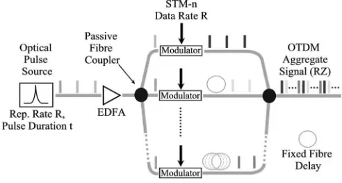
Fig. 1. Bit-interleaved OTDM transmission system.
result in a smaller number of channels operating at much higher data rates [2].
OTDM uses short optical pulses to represent data and multi-plexes in the time domain by allocating each channel specific bit slots in the overall multiplexed signal. The basic configuration for a bit-interleaved OTDM transmitter is shown in Fig. 1. The main component in a bit-interleaved OTDM system is an ultrashort optical pulse source. The optical pulse train generated is at a repetition rateRand is split intoN copies by a passive optical coupler, whereN corresponds to the number of electri-cal channels to be multiplexed. Each copy is then modulated by electrical data, which are at a data rate R. The resulting output from the modulator is an optical data channel where the electrical data are represented using short optical pulses. The modulated return-to-zero (RZ) optical signal then passes through a fixed fiber delay length, which delays each channel by 1/RN relative to adjacent channels in the system. This ensures that the optical data channels arrive at the output at a time corresponding to its allocated bit slot in the overall OTDM signal. TheN modulated and delayed optical data channels are then recombined using a second passive optical coupler to form the OTDM data signal.
To successfully operate at data rates in excess of 100 Gb/s per channel, new optical signal processing techniques such as optical demultiplexing [1] and optical sampling [3] will have to be developed. The majority of research has focused on taking advantage of optical nonlinearities that are present in fibers, semiconductors, and crystals, as these occur on timescales in
speed applications. However, there are a number of factors that may limit their performance for high-speed optical sig-nal processing. For those based on the Kerr effect in optical fibers, speciality fibers are required, and precise control of the wavelength of the control pulse and signal pulse around the zero-dispersion wavelength are necessary [4]. Gain depletion in semiconductor optical amplifiers (SOAs) limits the con-trol pulsewidth and, thus, the maximum switching speed [5], whereas those techniques employing second-harmonic gener-ation (SHG) in optical crystals require high optical intensities and adjustment of the crystal orientation for phase matching [6]. Due to these disadvantages, it is necessary to consider al-ternative optical nonlinearities for high-speed optical signal processing. This work will focus on the use of two-photon absorption (TPA) in a semiconductor for high-speed signal processing applications such as switching [7], sampling [8], autocorrelation [9], and optical thresholding [10].
This paper examines the use of TPA in a specially designed semiconductor microcavity for high-speed optical signal processing applications of autocorrelation, optical sampling, and optical switching. Section II presents a brief overview of the TPA process, with the specially designed microcavity presented in Section III. High-speed optical signal processing applications of autocorrelation, sampling, and switching via the TPA process in the semiconductor microcavity are demon-strated in Sections IV–VI, respectively. Section VII shows how the resonance response of the microcavity can be altered by angle tuning, thus providing wavelength selectivity for WDM and hybrid WDM/OTDM applications. Finally, Section VIII provides a summary of the experimental work carried out, followed by some conclusions.
II. TPA
TPA is a nonlinear optical-to-electrical conversion process that occurs in semiconductors when two photons are absorbed to generate a single electron–hole pairing. It occurs when a photon of energy Eph is incident on the active region of a semiconductor device with a band gap energy exceedingEph but less than2Eph. Under these conditions, individual photons do not possess sufficient energy to produce an electron–hole pair. However, an electron–hole pair can be produced by the simultaneous absorption of two photons, where the summation of the individual photon energies is greater than the band gap energy. The resulting photocurrent produced is proportional to the square of the incident optical power falling on the detector [11]. It is this nonlinear response, combined with TPA’s ultrafast response time (10−14s at 1550 nm [12]), that enables TPA to be considered for use in high-speed optical signal processing. The photocurrent produced via the TPA process in a semiconductor with single-photon absorption (SPA) coefficient
αand TPA coefficientβmay be represented by
J =eS hν
IabsSPA+1 2I
TPA abs
(1)
whereS is the illuminated area,hν is the photon energy, and
ISPA
[image:2.594.321.542.66.228.2]abs andIabsTPAare the SPA and TPA contributions in the total
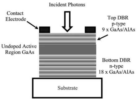
Fig. 2. Schematic of microcavity device structure.
absorption, respectively [13]. Therefore, to observe the TPA process, the semiconductor material is chosen, so that the band gap is greater than the energy of the incident photons but less than twice the photon energy. The nonlinear two-photon response is limited on the lower intensity side by SPA and on the high intensity side by the total absorption. The dynamic range where TPA can be usefully exploited for autocorrelation and demultiplexing applications is given by
α β ≤I≤
1
βL (2)
where L is the length of the absorption region, and I is the intensity of the light falling on the detector. As a result, TPA photogeneration will dominate, with only a residual amount of linear absorption due to lattice imperfections or the thermal excitations of carriers within the detector [11].
III. MICROCAVITYDEVICESTRUCTURE
One of the major problems associated with the use of TPA for optical signal processing applications such as autocorrelation, switching, and sampling is its inherent inefficiency, requiring either high optical intensities typically not found in an opti-cal communications network or a long interaction length for response enhancement [11]. One way in which the efficiency of the TPA process can be greatly enhanced is to place the active region within a semiconductor microcavity structure [14].
Fig. 3. Plot of the photocurrent generated as a function of incident optical wavelength.
band gap energy of 1.428 eV. The mirrors consist of alternating
λ/4 AlAs and λ/4 GaAs layers, with the top p-doped (C≈
1018 cm−3)mirror consisting of nine periods of AlAs/GaAs, whereas the bottom n-doped(Si≈1018cm−3)mirrors consists of 18 periods of AlAs/GaAs. The device length is designed to an integral of the absorption wavelength to enhance the TPA efficiency within the 1.5-µm wavelength range. The cavity lifetime of the device structure, which takes into account the reflectivity of the Bragg mirrors at either end of the device [15], is in the order of 1 ps.
Prior to carrying out an optical processing experiments using the devices fabricated, some initial characterization of the TPA microcavity samples was carried out. Fig. 3 shows a plot of the photocurrent generated from the microcavity as a function of the incident optical wavelength. The incident optical signal was generated from a commercially available 10-GHzu2ttunable mode-locked laser (TMLL) 1550 pulse source (pulse duration 2 ps, jitter<500 fs, tunable wavelength range 1480–1580 nm). The average optical output power was 0.5 mW, which was then optical amplified using a low-noise erbium-doped fiber amplifier (EDFA) to result in an incident peak power of 2 W falling on the TPA microcavity. The wavelength of the incident signal was then altered in steps of 0.5 nm, with the photocurrent generated by the TPA microcavity recorded using a picoamme-ter as a function of the incident wavelength. As can be seen in Fig. 3, the cavity response is dependent on the incident wavelength, with a cavity wavelength resonance of 1556 nm, with a measured spectral linewidth of 4.2 nm. Fig. 3 also shows that the peak wavelength resonance is three orders of magnitude greater when compared with the photocurrent generated for off-resonance wavelengths.
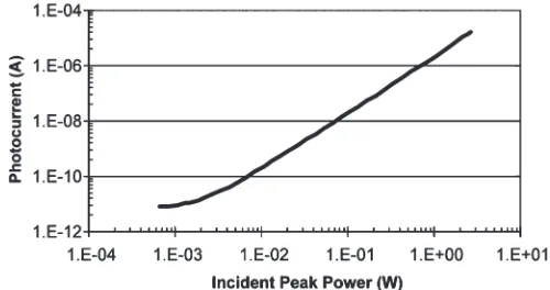
Fig. 4 shows a plot of the photocurrent generated as a func-tion of the incident peak optical power. The characterizafunc-tion was carried out using the same 10-GHz u2t tunable optical pulse source as used before, with the output wavelength tuned to coincide with the resonance peak wavelength of the cavity (1556 nm). The optical pulse train was then amplified using a low-noise EDFA (as before) before passing through an in-line power meter/attenuator, which allowed simultaneous power monitoring and attenuation of the optical signal. The incident signal was then attenuated from 16.4 dBm (average power) to
[image:3.594.299.549.71.203.2]−20 dBm in steps of 1 dB, with the TPA photocurrent generated measured using a picoammeter as a function of incident optical
Fig. 4. Plot of the photocurrent as a function of incident optical peak power at the cavity wavelength resonance.
power. Fig. 4 shows a square dependence of the photocurrent generated on the incident optical intensity, which is evidence of the TPA process, with residual SPA occurring at low energies. However, there is more than three orders of magnitude of nonlinear response with the current device.
IV. TPA-BASEDAUTOCORRELATION
The technique of autocorrelation allows the detection and characterization of ultrashort optical pulses. Here, results are presented that use a TPA microcavity as an unbiased “p-type, intrinsic, n-type” (PIN) diode, which exhibits nonlinear power-dependent response to detect and characterize mode-locked picosecond pulses as part of an autocorrelator. The use of the TPA microcavity completely replaces the nonlinear crystal and photomultiplier tube or photodetector needed for second-harmonic autocorrelation.
A. Principle of TPA Autocorrrelation
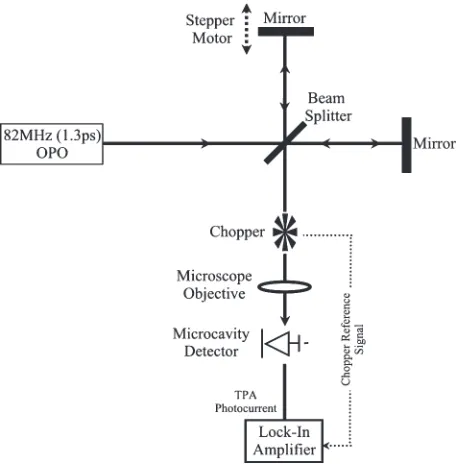
Fig. 5. Configuration of the TPA autocorrelator setup.
due to the vertical device orientation compared with waveguide TPA structures. The vertical nature and the relatively large area of the structure allow for easier fiber coupling than waveguide structures. In addition, the fact that the device is thin means there are no phase-matching problems compared with SHG crystals and free-space optics. In this section, we measured the sensitivity of the TPA microcavity devices in an autocorrelation configuration.
B. TPA Autocorrelation Experimental Setup
The noninterferometric autocorrelation is measured using a standard Michelson interferometer configuration. The con-figuration of a second-harmonic crystal followed by a highly sensitive photodetector used in the conventional schemes was simply replaced by the TPA microcavity photodetector. The experimental setup is shown in Fig. 5.
The optical pulses were generated by an optical parametric oscillator (OPO) synchronously pumped by a Ti:sapphire laser system, at a repetition rate of 82 MHz. At a wavelength of 1.5 µm, the typical temporal pulsewidth was 1.3 ps. After traversing the two arms of the interferometer, the two beams are colinearly focused to a 12-µm-diameter spot on the mi-crocavity device using a×10 microscope objective. The TPA photocurrent was measured using a lock-in technique. The best sensitivity is achieved using the shunt resistance RSHUNT=
10M·Ωof the microcavity device as the load resistor.
C. TPA Autocorrelation Experimental Results
The sensitivity of the TPA microcavity autocorrelator was measured by inserting neutral density filters in the beam path to control the signal-to-noise (SNR) levels. Fig. 6 shows the microcavity device photocurrent as a function of delay for an incident average power of 0.77 mW and peak power of 3.6 mW.
Fig. 6. Microcavity device photocurrent as a function of delay.
The quadratic response of the TPA photocurrent (versus incident average power) of the devices was verified down to 1-mW peak power. Given the nonlinear response of the photocurrent with incident power, it is possible to extrapolate the incident power to an SNR of 1 [21]. The sensitivity of the autocorrelator defined as the product of the peak and average power of the minimum detectable signal(SNR= 1)is found to be9.3×10−4(mW)2at a bandwidth of 1 Hz. For a given shunt resistanceRSHUNT, the limit for the detectable photocurrent is governed by the thermal noiseI2
th= 4kT BN/RSHUNT, where
kis the Boltzmann’s constant,T is the temperature, andBN =
1.6Hz is the measurement bandwidth. Comparing the theoreti-cal value of the thermal noise,Ith= 0.16pA, with the standard deviation of the data in the sidearms of the autocorrelation trace in Fig. 6,Ith= 0.1pA, we observe good agreement. To show the enhancement in sensitivity due to the microcavity, the au-tocorrelation measurement has also been performed at a wave-length of 1.46 µm off the stopband of the microcavity DBRs reflectivity spectrum. The magnitude of photocurrent measured offbandITPA= 220pA is consistent with the theoretical val-ues obtained by assuming TPA in bulk material with the same thickness as the active region of the microcavity device, given a TPA coefficient of β= 3×10⁻¹⁰ m/W. A sensitivity of
1.5×10³ (mW)2 is determined corresponding to an average power of 330 mW and peak power of 1.5 W. The sensitivity of the TPA microcavity autocorrelation measurements presented here compares very favorably with conventional autocorrelators based on SHG techniques, which typically have a sensitivity of 1(mW)2[22]. Compared with commercially available GaAsP photodiodes, AlGaAs LEDs, and GaAs LEDs recently used for TPA autocorrelation at 1.5µm, the microcavity device is found to be more sensitive by at least a factor of 10 [23] at a bandwidth of 1 Hz. However, waveguide devices and photomultiplier tubes are still more sensitive due to a much longer active region and direct-detection photon counting, respectively.
V. OPTICALSAMPLING
[image:4.594.307.553.68.210.2]permitting the accurate measurement of data rates approach-ing 40 Gb/s. Therefore, as individual channel data rates are expected to exceed this in the next 5–10 years, current electrical sampling techniques will be inadequate. Critical information such as pulse duration, pulse separation, and pulse rise time, which are crucial for the optimization of optical network per-formance, will be distorted.
A. Principle of TPA Sampling
TPA sampling employs a separate optical sampling pulse to monitor the performance criteria of a high-speed OTDM signal. The optical sampling pulse has a higher intensity and shorter duration[Isam(t−τ)]than the duration of the signal under test
[Isig(t)]. The signal and sampling pulses are then incident on the microcavity, with the electrical TPA signal generated[i(t)]
measured as a function of the sampling delayτ, resulting in an intensity cross-correlation measurement betweenIsam and
Isig[25], i.e.,
i(τ)∝ Isam(t−τ)Isig(t) (3)
where denotes time averaging. The sampling delay τ is generated by operating the sampling frequency(fsam)slightly detuned from a subharmonic of the signal frequency(fsig). The sampling frequency is calculated using [25]
fsam=
fsig
n+δ (4)
where n is an integer, and δ 1. This results in a scan frequency of
fscan=fsig
δ
δ+n (5)
which can be easily displayed on a standard high-impedance oscilloscope, with the measured signal representing the signal pulse waveform on a constant background [25].
B. TPA-Based Optical Sampling Experimental Setup
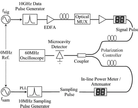
The TPA sampling setup is shown in Fig. 7. The signal pulseIsigis generated using the 10-GHzu2tTMLL 1550 pulse source already described in Section III. The sampling pulse
[image:5.594.305.548.66.256.2]Isam was generated using a Calmar Optcom Femtosecond Pulse Laser (pulse duration 500 fs, jitter < 140 fs, tunable range 1548–1558 nm). Both sources were tuned to the reso-nance wavelength of the TPA microcavity(λ= 1556nm)and were phase-locked together via the 10-MHz reference signal provided by the signal generators and the phase-locked loop (PLL) input to the Calmar source. The repetition rate of the signal pulse(fsig)was set to 9.998991 GHz with the sampling pulse(fsam) operating at 9.998992 MHz, resulting in a scan frequency (fscan) of 1 kHz. The 10-GHz optical pulse train used to create the data signal was first amplified using a low-noise EDFA before entering a passive delay line multi-plexer. The OTDM multiplexer is a commercially availableu2t 4-160 OMUX, consisting of four independently switchable stages with fixed fiber delay lengths within each stage. This
[image:5.594.305.546.299.361.2]Fig. 7. Experimental setup for optical sampling based on TPA in a semicon-ductor microcavity.
Fig. 8. Real-time TPA sampling measurement of (a) single optical pulse before multiplexing and (b) 100-GHz multiplexed pulse train.
results in the need to have an input signal at a repetition rate of exactly, or a multiple of, 9.95328 GHz (STM-64). Due to the narrow frequency locking range of the sampling pulse generator, it was not possible to generate a multiplexed optical signal at 160 GHz. However, by operating the signal and sam-pling pulse sources at the lowest repetition frequency possible (fsigandfsam), it was possible to generate a 100-GHz optical multiplexed pulse stream. This signal was then amplified a second time to overcome the 18-dB insertion loss associated with the passive multiplexer. The sampling and the signal pulses then pass through separate in-line power meters/attenuators and polarization controllers before being recombined at a passive optical fiber coupler. The power meters allow easy power mea-surement and attenuation of both pulse trains while allowing the system sensitivity to be continuously monitored. The combined signals are then incident on the microcavity, with the generated TPA photocurrent signal being displayed on a standard 60-MHz high-impedance digital oscilloscope.
C. TPA Sampling Results
Fig. 8(a) shows the real-time measurement of a single optical pulse as displayed on the high-impedance oscilloscope. The signal was measured prior to any optical multiplexing taking place. The optical pulse duration was measured to be 2.5 ps, with a pulsewidth of 2 ps expected. This deviation is due to the temporal resolution of the sampling setup. The temporal resolution is defined as
tres=
τ2
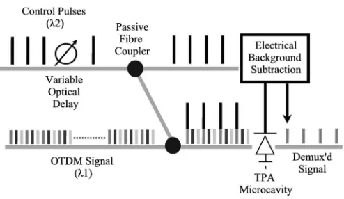
Fig. 9. Schematic of TPA demultiplexing.
and takes into account the cavity lifetime of the device
(τcavity= 1 ps) and the duration (tsam= 500 fs) and jitter
(jsam<140 fs) of the sampling pulse used. This gives a minimum temporal resolution of 1.1 ps. The average powers of the signal and sampling pulses used were 0.2 and 0.12 mW, respectively. Fig. 8(b) displays the real-time measurement of a 100-GHz (pulse separation 10 ps) optically multiplexed pulse train, with a signal average power of 0.17 mW and sampling average power of 0.16 mW. The variation in the amplitude of the optical pulses can be accounted for by the propagation of each pulse over a different transmission path within the passive delay line multiplexer. The sensitivity of the sampling system, which is defined as being the product of the peak power of the signal pulse and the average power of the sampling pulse [25], was calculated as 0.35(mW)2, corresponding to a signal peak power of 5.6 mW. This was obtained without any postampli-fication of the TPA photocurrent. With the addition of a low-noise amplifier after the microcavity, further improvements in the sensitivity are expected.
VI. OPTICALSWITCHING
In this section, a theoretical investigation into the possibility of high-speed optical demultiplexing using TPA in a micro-cavity is carried out. The main device parameters used in the model, such as the TPA coefficient, are taken from results obtained from the characterization of the microcavity samples used in the previous experimental work. Using this model, the operation of the demultiplexer is examined when various system parameters are varied.
A. TPA Optical Demultiplexer
The demultiplexer uses optical control pulses, operating at a different wavelength, to switch out data from a single high-speed OTDM system via the TPA effect in the microcavity [7]. By operating the control pulses at a different wavelength, inter-ference between control and data signal can be minimized [26]. The control pulses, which are at the repetition rate of the in-dividual channels in the multiplexed signal, are optically com-bined with the high-speed OTDM data signal and are incident on the device. The arrival time of the control pulses is varied using an optical delay line, so that they arrive at the demul-tiplexer at a time corresponding to the data to be switched out. A schematic of TPA demultiplexing is shown in Fig. 9. The TPA
between the OTDM data signal and the control pulses in the detector. Due to TPA’s nonlinear quadratic response, there is a strong contrast between the electrical TPA signal generated when the control and data pulses overlap on the detector and that generated when the adjacent channels arrive independently. The constant background signal due to the control pulses can be conveniently subtracted electrically, resulting in a high-contrast demultiplexing output signal. Thus, the TPA demul-tiplexer is able to carry out simultaneous channel selection and electrical detection in an OTDM optical communications system [7], [27].
Inasmuch as the generation of TPA electron–hole pairs is essentially instantaneous, the maximum switching speed is determined by the duration of the data and control pulses, allowing terabits/second data rates to become feasible [27]. It also allows for simpler optical alignment because it does not require phase matching as required for applications utilizing nonlinear crystals [28]. In addition, by making use of semicon-ductor microcavities, the inefficiency associated with TPA can be overcome.
B. Optical Demultiplexing Model
A simulation was carried out to determine the suitability of using a TPA microcavity for high-speed demultiplexing when a number of system parameters were varied. These parameters included the following:
• number of OTDM channels;
• ratio between peak power of control pulse and OTDM data pulse;
• electrical bandwidth of the TPA detector.
Fig. 10. BER versus control-to-signal power as the number of channels (with base rate of 10 Gb/s per channel) is varied.
The simulation models the switching scheme described in Fig. 9. An OTDM data signal is created, which consists of a number of individual data channels, each transmitting a pseudo-random bit stream (PRBS) signal. The optical pulsewidth used was kept to one quarter of the bit period of the overall aggregate OTDM data rate to avoid interference in adjacent channels. The number of channels, individual data rate, and peak power of the optical pulses used to represent the data are user-defined. Noise is then added to limit the optimum bit-error rate (BER) that can be achieved. The control pulses, which have the same duration as the data signal pulse, are combined and then incident on the TPA detector, which is modeled as per [11]. The peak power of the control pulses can be set to any value. From the resulting SNR [29], the optical bit-error rate (OBER) before the detector is calculated, which takes into account any noise in the transmitter, and the electrical bit-error rate (EBER), which is a function of device structure and device noise. The OBER is then compared with the EBER, with the overall goal being to determine the operating conditions such that the EBER is the same as the OBER. A more detailed description of the model can be found in [30].
C. Simulation Results
The first system parameter that was varied was the control-to-signal power ratio, as the number of channels were varied from 25 to 100, each with a data rate of 10 Gb/s per channel (250 Gb/s to 1 Tb/s aggregate OTDM data rates). The signal peak power was kept constant at 80 mW, and the detector bandwidth was set to 10 GHz,which is the minimum required to prevent intersymbol interference (ISI) between adjacent data bits in the demultiplexed channel.
Fig. 10 clearly shows that as the control-to-signal ratio is increased, the EBER approaches the OBER. This results from the fact that as the control-to-signal power is increased, the contrast ratio between the data signal synchronized with the control pulses, and those not synchronized widens. This reduces the amount of noise introduced by the adjacent channels, im-proving the SNR and the EBER. For a given control-to-signal power ratio, the EBER is degraded as the number of channels increases from 25 to 100. This results from the increased noise levels introduced from the increased number of channels. For a 25-channel system, the EBER reached the OBER for a control-to-signal ratio of 50:1, corresponding to a control pulse peak power of 4 W. During the initial characterization of the microcavity samples that were fabricated, a maximum
Fig. 11. BER versus control-to-signal power as electrical bandwidth is varied for a 250-Gb/s aggregate OTDM system.
peak optical power of 20 W was applied to the device without any damage being incurred. This suggests that a control pulse peak power of 4 W is well within the operating range of the microcavity structure, even if it is slightly large for practical applications.
Fig. 11 shows how the control-to-signal ratio is affected by the electrical bandwidth of the TPA microcavity. As already mentioned, by increasing the bandwidth of the device, the noise contribution due to the TPA photocurrent generated by adjacent OTDM channels falling within the response time of the device is reduced. This allows the same performance to be achieved, but at a reduced control-to-signal ratio. Hence, for the same system that is displayed in Fig. 10, the control-to-signal ratio can be reduced from 50:1 to 30:1, corresponding to a control pulse peak power of 2.4 W.
From recent experimental work carried out on the characteri-zation of the microcavities, the device bandwidth of the 100-µm sample was determined to be 1 GHz. It is hoped that with a smaller device size, an improved cavity design, and the use of high-speed packaging, the device bandwidth can be improved. As the device is based on a PIN structure, bandwidths in excess of 10 GHz should be readily feasible.
VII. ANGLETUNING OFTPA MICROCAVITY
Optoelectronic devices whose performance is enhanced by placing the active device structure inside a Fabry–Pérot reso-nant microcavity benefit from wavelength selectivity and the large increase of the resonant optical field introduced by the cavity. This resonance response makes the device suitable for WDM and hybrid WDM/OTDM applications, as the selection and optical signal processing functions (optical thresholding, switching, sampling, autocorrelation) of a high-speed optical data channel can be carried out simultaneously using a single device. In addition, by angle tuning the device, it is possible to vary the peak of the wavelength resonance. This technique would remove the need for expensive regrowth of different detectors for different WDM channels, as tilting the device alters the selected channel.
A. Principle of Angle Tuning
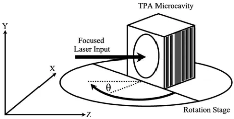
[image:7.594.297.551.74.180.2]Fig. 12. Schematic view of the angle-tuning setup including a TPA microcav-ity and translation stage.
Fig. 13. Measured and simulated peak wavelength responses of TPA micro-cavity versus incident light angle. The error bars show the variations in TPA and angles associated with the measurement system.
resonant wavelength, as the resonant conditions are strictly satisfied only for the normal component of the propagation constant. Using the transfer matrix model (TMM), we have ana-lyzed the reflection and transmission spectra of the microcavity structure and compare these with experimental results.
B. Angle Tuning Experimental Setup
A schematic cross-sectional view of the GaAs/AlAs micro-cavity structure is shown in Fig. 12. The micro-cavity resonance full-width at half-maximum (FWHM) was 4.2 nm with a finesse of 96. The created TPA photocurrent was measured using a standard lock-in amplifier technique. TPA photocurrent spectra are measured with various light incidence angles with a tunable OPO system. The light was focused onto the device using a 0.20 NA lens. The angle contribution due to the focusing effect is smaller than the accepting angle of the microcavity device.
C. Angle Tuning Experimental Results
Fig. 13 shows the resonance wavelength of the TPA micro-cavity as a function of incident angle. The resonance wave-length at normal incident for this device was 1.512 µm. By rotating the TPA microcavity by an angle θ, the resonance wavelength changes to lower wavelengths. The agreement be-tween theoretically predicted and the experimental results is excellent for θ less than ∼45◦. A tuning range of 35 nm is achieved by rotating the TPA microcavity over 45◦. Angle
Fig. 14. Measured and simulated responses of TPA microcavity at 1.52µm versus incident light angle.
tuning beyond 45◦ is possible, but we were limited to 45◦ by the tuning range of our rotation stage.
In Fig. 14, the incident wavelength was tuned to cavity resonance, corresponding to peak TPA-induced photocurrent and kept constant, whereas the incident angle was varied. The change in angle of incidence off normal leads to a decrease of the TPA response that can be easily explained by the TMM ap-proach. The FWHM of the angular response of the TPA device for a constant wavelengthλ0is 15.3◦. Here,λ0is the resonant wavelength for normal incident. The results agree well with the theoretical predictions made for plane waves using the TMM.
VIII. SUMMARY OFRESULTS
[image:8.594.45.291.227.372.2]ratio of 30:1 and an electrical device bandwidth of 30 GHz. This bandwidth should be feasible with a smaller device size, an improved cavity design, and the use of a high-speed packaging as the microcavity is based on a PIN structure. Finally, it was reported that with the use of device angle tuning, the wavelength resonance of the microcavity could be shifted by up to 35 nm with a rotation of 45◦. This ability to alter the peak wavelength resonance of a single device would make it suitable for WDM and hybrid WDM/OTDM applications without the need for growth of different devices for different wavelength channels.
IX. CONCLUSION
This paper has shown that by incorporating a microcavity design, TPA efficiency can be improved to allow practical optical signal processing at power levels typically found in an optical communications network. Therefore, by developing a specially designed microcavity device, TPA-based elements could form one of the major building blocks of an optical subsystem designed to carry out optical signal processing tasks in the next generation of optical systems.
REFERENCES
[1] D. M. Spirit, A. D. Ellis, and P. E. Barnsley, “Optical time division multiplexing: Systems, networks,”IEEE Commun. Mag., vol. 32, no. 12, pp. 56–62, Dec. 1994.
[2] M. Attygalle, H. F. Liu, and A. Nirmalathas, “An all-optical WDM to TDM conversion scheme with simultaneous all-optical synchronization for WDM/OTDM network nodes,”Opt. Quantum Electron., vol. 33, no. 7, pp. 827–840, 2001.
[3] S. Kawanishi, “Ultrahigh-speed optical time-division-multiplexed trans-mission technology based on optical signal processing,”IEEE J. Quantum Electron., vol. 34, no. 11, pp. 2064–2079, Nov. 1998.
[4] M. Saruwatari, “All-optical signal processing for terabit/second optical transmission,”IEEE J. Sel. Topics Quantum Electron., vol. 6, no. 6, pp. 1363–1374, Nov./Dec. 2000.
[5] G. P. Agrawal,Applications of Nonlinear Fiber Optics, 1st ed. New York: Academic, 2001.
[6] P. Staudt, “Getting the measure of ultrashort pulses,”Opto Laser Europe, no. 120, pp. 33–35, Sep. 2004.
[7] B. C. Thomsen, J. D. Harvey, and L. P. Barry, “Error free demultiplex-ing in high-speed OTDM systems usdemultiplex-ing a two-photon absorption based switch,” inProc. Opt. Fibre Commun. Conf., 2001, p. W02-1.
[8] K. Kikuchi, “Optical sampling system at 1.5µm using two photon absorp-tion in Si avalanche photodiode,”Electron. Lett., vol. 34, no. 13, pp. 1354– 1355, Jun. 1998.
[9] Y. Takagi, T. Kobayashi, and K. Yoshihara, “Multiple- and single-shot autocorrelator based on two-photon conductivity in semiconductors,”Opt. Lett., vol. 17, no. 9, pp. 658–660, May 1992.
[10] Z. Zheng, A. M. Weiner, J. H. Marsh, and M. M. Karkhanehchi, “Ultrafast optical thresholding based on two-photon absorption GaAs waveguide photodetectors,”IEEE Photon. Technol. Lett., vol. 9, no. 4, pp. 493–495, Apr. 1997.
[11] H. Folliot, M. Lynch, A. L. Bradley, T. Krug, L. A. Dunbar, J. Hegarty, J. F. Donegan, and L. P. Barry, “Two-photon-induced photoconductivity enhancement in semiconductor microcavities: A theoretical investiga-tion,”J. Opt. Soc. Amer. B. Opt. Phys., vol. 19, no. 10, pp. 2396–2402, Oct. 2002.
[12] J. Donegan, “Two-photon absorption speeds optical switching,”Lightw. Europe, vol. 1, no. 5, p. 31, Jul. 2002.
[13] F. R. Laughton, J. H. Marsh, D. A. Barrow, and E. L. Portnoi, “The two photon absorption semiconductor waveguide autocorrelator,”IEEE J. Quantum Electron., vol. 30, no. 3, pp. 838–845, Mar. 1994.
[14] H. Folliot, M. Lynch, A. L. Bradley, L. A. Dunbar, J. Hegarty, J. F. Donegan, L. P. Barry, J. S. Roberts, and G. Hill, “Two-photon absorption photocurrent enhancement in bulk AlGaAs semiconductor mi-crocavities,”Appl. Phys. Lett., vol. 80, no. 8, pp. 1328–1330, Feb. 2002.
[15] T. Krug, M. Lynch, A. L. Bradley, J. F. Donegan, L. P. Barry, H. Folliot, J. S. Roberts, and G. Hill, “High-sensitivity two-photon ab-sorption microcavity autocorrelator,”IEEE Photon. Technol. Lett., vol. 16, no. 6, pp. 1543–1544, Jun. 2004.
[16] H. K. Tsang, L. Y. Chan, J. B. D. Soole, H. P. LeBlanc, M. A. Koza, and R. Bhat, “High sensitivity autocorrelation using two-photon absorption in InGaAsP waveguides,”Electron. Lett., vol. 31, no. 20, pp. 1773–1775, Sep. 1995.
[17] Y. Takagi, “Simple autocorrelator for ultraviolet pulse width measure-ments based on the nonlinear photoelectric effect,”Appl. Opt., vol. 33, no. 27, pp. 6328–6332, Sep. 1994.
[18] J. K. Ranka, A. L. Gaeta, A. Baltuska, M. S. Pshenichnikov, and D. A. Wiersma, “Autocorrelation measurement of 6-fs pulses based on the two-photon-induced photocurrent in a GaAsP photodiode,”Opt. Lett., vol. 22, no. 17, pp. 1344–1346, Sep. 1997.
[19] D. T. Reid, M. Padgett, C. McGowan, W. E. Sleat, and W. Sibbett, “Light-emitting diodes as measurement devices for femtosecond laser pulses,”
Opt. Lett., vol. 22, no. 4, pp. 233–235, Feb. 1997.
[20] D. T. Reid, B. C. Thomson, J. M. Dudley, and J. D. Harvey, “Sono-gram characterisation of picosecond pulses at 1.5 mm using waveguide two photon absorption,”Electron. Lett., vol. 36, no. 13, pp. 1141–1142, Jun. 2000.
[21] T. Krug, M. Lynch, A. L. Bradley, and J. F. Donegan, “Two-photon absorption in microcavities for optical autocorrelation and sampling,” in
Tech. Proc., CLEO/Europe-EQEC Conf., Munich, Germany, p. 258. [22] APE,Autocorrelator PulseScope Manual, 2001.
[23] L. P. Barry, B. C. Thomsen, J. M. Dudley, and J. D. Harvey, “Autocor-relation and ultrafast optical thresholding at 1.5µm using a Commercial InGaAsP 1.3µm laser diode,”Electron. Lett., vol. 34, no. 4, pp. 358–360, Feb. 1998.
[24] R. L. Jungerman, G. Lee, O. Buccafusca, Y. Kaneko, N. Itagaki, and R. Shioda,Optical Sampling Reveals Details of Very High Speed Fiber Systems. Palo Alto, CA: Agilent Technologies, 2004, pdf document. [Online]. Available: http://www.agilent.com
[25] B. C. Thomsen, L. P. Barry, J. M. Dudley, and J. D. Harvey, “Ultra sensitive all-optical sampling at 1.5µm using waveguide two-photon absorption,”Electron. Lett., vol. 35, no. 17, pp. 1483–1484, Aug. 1999. [26] Y. Tanaka, N. Sako, S. Imoto, and T. Kurokawa, “Profilometry using
optical microwaves with different carrier frequencies and two-photon ab-sorption process of photodetector,”IEEE Photon. Technol. Lett., vol. 17, no. 12, pp. 2682–2684, Dec. 2005.
[27] B. C. Thomsen, L. P. Barry, J. M. Dudley, and J. D. Harvey, “Ultrahigh speed all-optical demultiplexing based on two-photon absorption in a laser diode,”Electron. Lett., vol. 34, no. 19, pp. 1871–1872, Sep. 1998. [28] T. Hori, N. Nishizawa, M. Yoshida, and T. Goto, “Cross-correlation
mea-surement without mechanical delay scanning using electronically con-trolled wavelength-tunable femtosecond soliton pulse,” Electron. Lett., vol. 37, no. 17, pp. 1077–1078, Aug. 2001.
[29] G. P. Agrawal,Fiber-Optic Communication Systems, 1st ed. San Diego, CA: Academic, 1997.
[30] P. J. Maguire, L. P. Barry, T. Krug, M. Lynch, A. L. Bradley, J. F. Donegan, and H. Folliot, “Simulation of a high-speed demultiplexer based on two-photon absorption in semiconductor devices,”Opt. Commun., vol. 249, no. 4–6, pp. 415–420, May 2005.
[31] Z. Ruikang, Z. Yuan, Z. Wei, X. Yingqiang, D. Yun, H. Yongqing, R. Xiaomin, N. Zhichuan, and W. Ronghan, “Angular dependent char-acteristics of a 1.3 µm GaInNAs/GaAs quantum-well resonant cavity enhanced photodetectors,”Microw. Opt. Technol. Lett., vol. 34, no. 5, pp. 333–336, 2002.
[32] M. Unlu and S. Strite, “Resonant cavity enhanced photonic devices,”
J. Appl. Phys., vol. 78, no. 2, pp. 607–639, Jul. 1995.
P. J. Maguire(M’01) was born in Dublin, Ireland, in 1978. He received the B.Eng. degree in electronic engineering (First Class Honors) and the Ph.D. degree in electronic engineering from Dublin City University (DCU) in 2001 and 2006, respectively. His Ph.D. dissertation was entitled “Optical pulse generation and signal processing for the development of high-speed OTDM networks.”
the M.Eng.Sc. degree in optical communications from the University College Dublin, Dublin, Ireland, in 1991 and 1993, respectively, and the Ph.D. degree in physics from the University of Rennes, Rennes, France, in 1996.
From February 1993 to January 1996, he was employed as a Research Engineer in the Optical Systems Department of France Telecom’s Research Laboratories (CNET), Lannion, France. During this period, his research in-volved the use of ultrashort optical pulses in high-capacity optical networks. In February 1996, he joined the Applied Optics Centre, Auckland University, Auckland, New Zealand, as a Research Fellow. His work in New Zealand was mainly concerned with optical pulse generation and measurement as well as the use of optical nonlinearities for high-speed all-optical switching in fiber networks. In March 1998, he took up a lecturing position in the School of Electronic Engineering at Dublin City University, where he has since developed the Radio and Optical Communications Laboratory.
T. Krugreceived the Diploma in physics from Technische Universität Dresden, Dresden, Germany, in 2001 and the Ph.D. degree in physics in the area of semiconductor microcavities from Trinity College, Dublin, Ireland, in 2006.
He joined the Semiconductor Optronics Group in Trinity College in 2001. Since 2006, he has become a Research Fellow with Nelson Mandela Metropol-itan University, Port Elizabeth, South Africa. His current work is focused on properties of metal-organic vapor-phase epitaxy-grown InAs and InAsSb for IR detectors.
W. H. Guowas born in Hubei Province, China, in 1976. He received the B.Sc. degree in physics from Nanjing University, Nanjing, China, in 1998 and the Ph.D. degree in physics/semiconductor from the Institute of Semiconductors, Chinese Academy of Sciences, Beijing, China, in 2004, with a dissertation on studying the finite-difference time-domain simulation and fabrication of optical microcavities and semiconductor optical amplifiers.
Since September 2004, he has been a Postdoctoral Researcher at the Depart-ment of Physics, Trinity College, Dublin, Ireland.
J. O’Dowdwas born in Sligo, Ireland, on May 27, 1981. He received the B.A. mod degree in physics from the University of Dublin, Trinity College, Dublin, Ireland, in 2004. He is currently working toward the Ph.D. degree in physics at the same university.
His research interests include the use of two-photon absorption for optical performance monitoring of transparent networks.
University, Dublin, Ireland, in 1986.
He is currently a Senior Researcher with the Semiconductor Photonics Group, Department of Physics, University of Dublin, Trinity College, Dublin, Ireland. His current research interests include nonlinear optics in semiconductor microcavities and laser diode gas sensing.
A. L. Bradleyreceived the B.Sc. degree from the University College Dublin, Dublin, Ireland, in 1992 and the M.Sc. and Ph.D. degrees from Trinity College, Dublin, in 1994 and 1998, respectively, all in physics.
She was a Postdoctoral Researcher at Trinity College and a Lecturer at the Institute of Technology, Tallaght, before taking up her current position as a Lecturer at the School of Physics, Trinity College, in 2001. Her current research interests include microcavity physics and applications, the dynamical properties of semiconductor optical amplifiers, semiconductor nanocrystal dynamics, and novel wideband gap materials.
J. F. Donegan(M’04) received the B.Sc. and Ph.D. degrees from the National University of Ireland, Galway, Ireland, in 1982 and 1986, respectively, both in physics.
He had postdoctoral positions at Lehigh University Bethlehem, PA, and Max Planck Institut fuer Festkoerperforschung, Stuttgart, Germany. He is currently a Professor of physics at Trinity College, Dublin, Ireland. He has 120 publica-tions. His research area is photonics with the following subthemes: 1) quantum-dot cellular interactions for biomedical applications, 2) nonlinear microcavity photodetectors for optical performance monitoring, 3) tunable diode lasers based on the slotted Fabry–Pérot cavity, 4) optical sensing applications with tunable diodes, and 5) microsphere and microtube structures for microlaser and microsensor development.
H. Folliotreceived the engineer diploma and the Ph.D. degree in physics from INSA, Rennes, France, in 1995 and 1999, respectively. His Ph.D. dissertation involved the study of the quantum-confined Stark effect in InGaAs–InP quan-tum wells and microcavities for holographic beam steering applications.