Multi-task control strategy for grid-tied
1inverters based on Conservative Power Theory
2Dr. Fernando P. Marafão
3
UNESP–Univ. Estadual Paulista, SP, Brazil
4
Postal address: Group of Automation and Integrated Systems, Av. Três de Março 511 - Sorocaba, Brazil
5
fmarafao@sorocaba.unesp.br
6
Msc. Danilo I. Brandão
7
State University of Campinas, SP, Brazil
8
Postal address: Department of Energy System and Control, Av. Albert Eintein 400, - Campinas, Brazil
9
dbrandao@dsce.fee.unicamp.br
10
Dr. Alessandro Costabeber
11
University of Nottingham, NG, UK
12
Postal address: Department of Electrical and Electronic Engineering, NG7 2RD, Nottingham, UK
13
alessandro.costabeber@nottingham.ac.uk
14
Dr. Helmo K. M. Paredes
15
UNESP–Univ. Estadual Paulista, SP, Brazil
16
Postal address: Group of Automation and Integrated Systems, Av. Três de Março 511 - Sorocaba, Brazil
17
hmorales@sorocaba.unesp.br
18
Abstract—In recent years, the concept of decentralizing power generation through the deployment of
19
distributed generators (DGs) has been widely accepted and applied, driven by the growing market of
20
renewable energy sources, in particular photovoltaic, wind and small hydro. These distributed generators are
21
normally equipped with a switching power interface (inverter), acting as front end with the grid. In this
22
scenario this paper proposes a multi-task control strategy for distributed generation inverters that
23
simultaneously allows the DG system to inject the available energy, as well as to work as a voltage drop
24
compensator or as an active power filter, mitigating load current disturbances and improving power quality of
25
the grid. The main contribution of the proposed system, with respect to other solutions in the literature, is that
26
the proposed control loops are based on the Conservative Power Theory decompositions. This choice provides
27
decoupled power and current references for the inverter control, offering a very flexible, selective and
28
powerful control strategy for the DG system. The paper also discusses the choice of the current waveform for
29
injecting/absorbing active power into/from the grid, and both sinusoidal and resistive references have been
30
compared in terms of damping capability. Finally, simulation and experimental results are provided in order
31
to validate the proposed functionalities of the DG control system.
I. INTRODUCTION 1
Distributed generation systems (DGS) have drawn considerable attention in the last two
2
decades, mainly for the increasing concerns about the continuous expansion of world energy
3
demand and the consequent CO2 emissions [1,2]. In addition to environmental support, DGSs 4
also provide some other desirable features, such as lower infrastructure costs, energy
5
diversification and deregulation of energy market. Moreover, some DGSs - e.g. those based on
6
photovoltaic - can be installed close to the loads, reducing distribution losses and increasing
7
hosting capacity with minimum infrastructure investments. Another important issue for power
8
systems industry is power quality (PQ) control over the network, especially in presence of
9
reactive, nonlinear and/or unbalanced loads [3-10], and DGS can be a valuable support by
10
exploiting their inherent power control capability and flexibility. In fact, most of the DGSs are
11
equipped with switching power interface (SPI) [11], which may be used to enhance power
12
quality in steady state operation and/or during transient events, instead of only injecting active
13
power into the grid [12-14]. In this context, this paper proposes a DGS control architecture
14
capable of injecting the available energy into the grid and, simultaneously, to work as a static
15
compensator providing voltage support at the point of common coupling (PCC) or as an active
16
power filter (APF), mitigating the detrimental effects of distorted load currents.
17
This paper considers a grid-tied single-phase inverter, representing a common grid front end
18
in residential photovoltaic installations. The same approach can be extended to three-phase
19
systems. The reason for choosing the single-phase inverter is based on the limited complexity of
20
its conversion system, which allows a detailed discussion of the proposed multi-task controller,
21
as well as the fact that single-phase inverters are the most common topologies for low voltage
22
distribution systems. The main contribution of this paper is related with the utilization of the
23
Conservative Power Theory (CPT) [15] to propose an alternative inverter control strategy for
24
distributed generation systems. Based on time-domain definitions, active, reactive and harmonic
25
current injection can be performed selectively, independently of waveform distortions. As
26
already mentioned, the tasks performed by the controller are:
27
1. Active power injection/absorption, to fully exploit the distributed energy resources;
2. Voltage regulation, to provide voltage support at a given PCC, by means of controlling
1
the reactive power injection;
2
3. Selective compensation, to minimize load current disturbances, by means of harmonic
3
and/or reactive current compensation.
4
Active power injection is based on an equivalent circuit conductance and can be set as a
5
sinusoidal current or a resistive current, independently on the presence of grid voltage
6
distortion. The voltage drop compensation is based on the injection of reactive current by means
7
of a controlled equivalent reactivity. Active filtering is naturally performed by the current
8
control of the inverter when the proper current reference has been calculated using CPT. The
9
functionalities of the active compensator become very flexible due to the possibility of being
10
performed selectively [16]. This feature is powerful, especially when the DGS operates close to
11
its power/current limits, where the prioritization of specific electrical disturbance compensation
12
becomes relevant and useful.
13
Beyond its flexibility and selectivity, the proposed method differs from others existing
14
solutions for the fact that it doesn’t need any kind of reference-frame transformation (as [5] and
15
[6]); discrete Fourier transformer (as [7]); Instantaneous Power Theory (as [8]) or
16
synchronization algorithm (as [9] and conventional harmonic current compensation), which
17
might show nontrivial power control errors, slow dynamic response, DC real and reactive power
18
bias or inaccuracy under distorted voltages. The proposed method does not need a
19
synchronization algorithm, and therefore its dynamic response and steady state performance are
20
related only with the designed voltage and current controllers.
21
Even if recent controllers overcome most of the limitations suffered in the past, it is also
22
worth to mention that the computation complexity of the proposed method is limited to the
23
discrete implementation of the controller and to two divisions needed to calculate the CPT
24
equivalent conductance and reactivity. As shown in section VI, the control strategy has been
25
implemented in a fixed-point digital signal processor (DSP), without encountering particular
26
issues.
II. CONSERVATIVE POWER THEORY–BRIEF REVIEW FOR SINGLE-PHASE SYSTEMS 1
The Conservative Power Theory, proposed by Tenti et al. in [15], is defined in time domain
2
for general (sinusoidal or non-sinusoidal) operating conditions, and can be applied to
single-3
phase and poly-phase systems, with or without neutral conductor. The CPT proposes an
4
orthogonal decomposition of current and power in the stationary (abc) frame, according to terms
5
which are directly related to the load electrical characteristics, such as: average power transfer,
6
reactive energy, nonlinearities and unbalances.
7
Assuming a single-phase circuit under periodic operation, whereݒ,݅andݒොare, respectively,
8
the instantaneous values of voltage, current and the unbiased voltage integral - i.e. the AC
9
component of the voltage integral-, the CPT defines the instantaneous active power () and the
10
instantaneous reactive energy (ݓ) and their average values as:
11
ܲ==〈ݒ,݅〉=ܶන ݒ1 (ݐ).݅(ݐ)݀ݐ
்
;
ܹ =ݓ =〈ݒො,݅〉=1ܶන ݒො(ݐ).݅(ݐ)݀ݐ
்
.
(1)
Such quantities are conservative in every electrical network, independently on current and
12
voltage waveforms. The only requirement is a steady-state periodic operation. Moreover, by
13
using the CPT, the PCC instantaneous total current can be decomposed into active current (݅),
14
non-active current (݅), reactive current (݅) and void current (݅௩), as following:
15
݅=݅+݅=݅+݅+݅௩ . (2)
The active current has been defined as:
16
݅=‖ݒܲ‖ଶ.ݒ=ܩ.ݒ, (3)
whereܩrepresents the load equivalent conductance and ‖ݒ‖means the voltage Euclidian norm
17
or RMS value. The non-active current (݅) is the remaining part of the total current and it is
18
calculated by the difference:
19
݅=݅−݅ . (4)
The reactive current has been defined as:
݅=‖ݒොܹ‖ଶ.ݒො=ܤ.ݒො, (5)
whereܤrepresents the load equivalent reactivity and‖ݒො‖is RMS value of the unbiased voltage
1
integral. The void current is the residual term, which depends on the voltage and the current
2
distortion (harmonics):
3
݅௩=݅−݅=݅−݅−݅ . (6)
This current does not convey active power nor reactive energy, and reflects the presence of
4
harmonic scattering and current harmonics generated by the load [15,17].
5
By definition, all the terms are orthogonal (decoupled) to each other. Then:
6
‖݅‖ଶ=‖݅
‖ଶ+‖݅‖ଶ+‖݅௩‖ଶ . (7)
Thus, the apparent power may be calculated as:
7
ܣଶ=‖ݒ‖ଶ.‖݅‖ଶ=ܲଶ+ܳଶ+ܦଶ . (8)
The active power (ܲ) is related to the average power transfer. The reactive power (ܳ) is
8
related to the reactive energy and the void power (ܦ) is related to the current and voltage
9
distortions (nonlinearities). Unlike the active power and reactive energy, the apparent, reactive
10
and void powers are non-conservative quantities [15].
11
Finally, the power factor is calculated as following:
12
ߣ=ܲ
ܣ . (9)
The previous definitions can be extended to three-phase circuits as shown in [15]. Note that
13
all the equations are valid independently on the grid voltage waveform, which could also be
14
distorted or unbalanced (three-phase case).
15
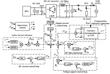
III. PROPOSED MULTI-TASK CONTROLLER 16
The proposed multi-task controller is capable to: 1) generate sinusoidal or resistive active
17
current injection/absorption; 2) provide voltage support managing reactive power and 3)
18
selective reactive and void current compensation.
19
Fig. 1 indicates the block diagram of a generic distributed single-phase generation system
20
including the power circuit and its control scheme. The left side block (RES) represents any sort
focuses on the DC-AC inverter control strategy, which is based on three main control loops
1
required to perform the inverter functionalities.
2
Theoutput current control loopis responsible for injecting the desired inverter current (݅௩∗ )
3
at the PCC. The DC link control loop regulates the DC link voltage. The DC current control
4
loopguarantees that the inverter output current does not present any DC component (MAmeans 5
moving average filter). These last two control loops are decoupled from the first one assuming a
6
design that ensures adequate difference between the respective crossover frequencies.
7
Note that in Fig. 1 there is a supervisory control block, an additional degree of freedom
8
enabling the definition of the voltage waveform used in thecurrent decomposition by theCPT
9
block,DC link control loop(ݒᇱכ) andactive current reference(ݒᇱᇱכ). These voltage signals can
10
correspond either to the measured PCC voltage (ݒ) or to its fundamental component (ݒ ).
11
In the following sub-sections, the main parts of the control scheme in Fig.1 will be described to
12
highlight their role in the proposed multi-task control approach.
13
[image:6.595.74.512.406.703.2]14
A. Active current reference generation
1
From the scheme in Fig. 1, the controllable active current reference to be injected/absorbed
2
(݅∗) comes from the equivalence conductance (ܩ), which is based on the PCC voltage and on
3
the available power (ܲோாௌ) to be transferred from the RES to the AC grid. The waveform of this
4
current reference can be calculated either from the measured PCC voltage (ݒ) or from its
5
fundamental component (ݒ ), leading to resistive (RCI) or sinusoidal (SCI) current injection,
6
respectively. Under certain conditions and from the power quality point of view, the results of
7
these two injection strategies may be significantly different, as discussed later in section IV and
8
V.
9
Note that (݅∗) refers to the controllable component of the active current, added to the active
10
current component coming from theDC link control loop (݅ௗ∗ ), that guarantees the DC voltage
11
regulation through power balance between RES and grid. Also for (݅ௗ∗ ), the current waveform
12
absorbed from the grid can be either resistive (RCA) or sinusoidal (SCA), depending on the
13
voltage reference. Note that the signal ofܲோாௌdefines the direction of the active power flow. It
14
must be observed that the DC link control loop is normally enough to guarantee the power
15
balance between the RES and the grid, but when the information onܲோாௌis available from the
16
source, the generation of the additive term (݅∗) acts as a feed-forward control term improving
17
the dynamics of the DC link voltage regulation.
18
B. Compensation reference generator
19
As previously mentioned, the CPT can provide the current reference (்݅∗ ) to compensate,
20
selectively or not, the load current disturbances [16]. So, each decomposed current term (݅,݅
21
and݅௩) can define a different compensation strategy, which can be included on the DGS in order
22
to maximize its utilization and improve the power quality at the PCC. Of course, the DGS
23
compensation functionality should be activated only when the system is not using the full
24
inverter capability to inject active power into the grid or in case of other financial or technical
25
constraints [3].
Moreover, since the main CPT current decompositions (active and reactive currents) are
1
based on the concepts of proportionality and orthogonality with respect to a certain voltage
2
reference, such voltage choice is crucial. Thus, if the PCC measured voltage is directly used for
3
the CPT decompositions, after compensating the non-active load current the equivalent system
4
(loads plus DG) is seen by the grid as an equivalent resistive load, absorbing a current
5
proportional to the instantaneous grid voltage waveform, including all the harmonics. On the
6
other hand, if the voltage fundamental component is used for the CPT decompositions, the
7
result after the compensation is a pure sinusoidal current, in phase with the fundamental voltage.
8
These two active compensation approaches are known as resistive load synthesis (RLS) and
9
sinusoidal source current synthesis (SSC) and under certain circumstances, they might lead to
10
quite different results [18,19]. It is important to highlight that both the RLS and SSC
11
compensation approaches are based on the CPT current decomposition.
12
Sections V and VI will compare and discuss the results when RLS or SSC injection strategy is
13
adopted by the DG control system.
14
C. Voltage support reference
15
Thevoltage support control loopinjects reactive current (݅௩௦∗ ) at the PCC to keep the voltage
16
within a predefined profile. The concept of voltage regulation through reactive power injection
17
using distributed inverters was first proposed in [20], where a droop function was also included
18
to prevent interactions between multiple inverters acting on the same feeder. In the multi-task
19
controller, the output of the voltage support controller [ܥ௩௦(ݏ)] corresponds to an equivalent
20
reactivity (ܤ), which is needed to retain the PCC voltage within the desired level. Depending
21
on the sign of the controller output, the resulting reactive current reference (݅௩௦∗ ) can either
22
increase or decrease the PCC voltage level, allowing dynamic voltage regulation [21].
23
However, similarly to the harmonic currents compensation, the voltage support functionality
24
can be activated only when the DG is not injecting its nominal power into the grid or in case of
25
particular financial or technical constraints.
26
It must be pointed out that the dynamic voltage support performed by injecting reactive power
27
with the DG requires the additional hypothesis of operating the DG in a grid with inductive
cables. Instead, if the cables are mainly resistive, the injection/absorption of more reactive
1
power than the amount needed to feed the reactive demand of the local load would mainly result
2
in additional losses, instead of in voltage variations. In this sense, the proposed solution is more
3
suitable for three-phase converters connected to medium voltage systems, where the hypothesis
4
is verified.
5
D. Further considerations about the mult-task control scheme
6
Except for theoutput current control loop[ܥ(ݏ)], all the controllers in Fig.1 are based on PI
7
regulators, designed with classical methods, such as frequency response analysis [22]. Table I
8
reports the basic parameters and the corresponding controllers information, where ݂ and PM
9
are the designed crossover frequency and phase margin. Instead, for the output current control
10
loop, a proportional plus resonant controller has been applied and designed as discussed in [23].
11
All odd harmonics from the fundamental to the eleventh order have been included as resonant
12
terms.
13
It is important to highlight that the proposed multi-task control may be equally applied for
14
different power and voltage rating or in a three-phase system, simply changing the design of the
15
passive and active devices and the controller gains. It is also independent on the specific RES.
16
TABLE I. SYSTEM AND CONTROLLERS SPECIFICATIONS. 17
DC-AC converter
P=1.5kVA; Vac=127V; Vdc=235V; Lf=1.5mH; Rf=0.056Ω; Cf=2μF.
Ci(s) Cvi(s) Cvs(s) Cidc(s)
fc=1kHz;
PM=60°.
fc=1Hz;
PM=50°.
fc=5Hz;
PM=75°.
fc=20Hz;
PM=75°.
18
IV. ANALYSIS OF THE DISTRIBUTED GENERATOR ON DAMPING HARMONIC RESONANCES 19
This section attempts to investigate the influence of the distributed generator (DG) on the
20
system frequency response, when the inverter is controlled to inject or absorb active power and
21
at the same time acts as an active power filter. Fig. 2.a and Table II show the proposed circuit
22
and related parameters chosen for the analysis.
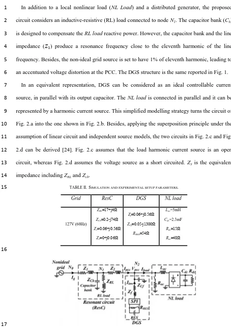
In addition to a local nonlinear load (NL Load) and a distributed generator, the proposed
1
circuit considers an inductive-resistive (RL) load connected to nodeN1. The capacitor bank (Cb) 2
is designed to compensate theRL loadreactive power. However, the capacitor bank and the line
3
impedance (ܼଵ) produce a resonance frequency close to the eleventh harmonic of the line
4
frequency. Besides, the non-ideal grid source is set to have 1% of eleventh harmonic, leading to
5
an accentuated voltage distortion at the PCC. The DGS structure is the same reported in Fig. 1.
6
In an equivalent representation, DGS can be considered as an ideal controllable current
7
source, in parallel with its output capacitor. TheNL loadis connected in parallel and it can be
8
represented by a harmonic current source. This simplified modelling strategy turns the circuit of
[image:10.595.54.508.63.706.2]9
Fig. 2.a into the one shown in Fig. 2.b. Besides, applying the superposition principle under the
10
assumption of linear circuit and independent source models, the two circuits in Fig. 2.c and Fig.
11
2.d can be derived [24]. Fig. 2.c assumes that the load harmonic current source is an open
12
circuit, whereas Fig. 2.d assumes the voltage source as a short circuited. Z3 is the equivalent 13
impedance includingZRLandZcb. 14
TABLE II. SIMULATION AND EXPERIMENTAL SETUP PARAMETERS. 15
Grid ResC DGS NL load
127V (60Hz)
ZRL=17+j4Ω
ZCb=0.2-j74Ω
Z1=0.06+j0.56Ω
Z2=0+j0.06Ω
Zf=0.06+j0.56Ω
ZCf=0.05-j1300Ω
RRES=54Ω
Lac=5mH
Cdc=2.3mF
Rdc=15Ω
Rac=48Ω
16
17
[image:10.595.159.438.441.707.2]1
(b) Equivalent circuit of the circuit configuration. 2
[image:11.595.59.499.73.459.2](c) equivalent circuit without load harmonic current. (d)equivalent circuit without voltage source.
Fig. 2. Circuits and equivalent circuits from superposition analysis of the simulation and experimental circuit. 3
A. Active power absorption
4
In order to analyze the effect of the DGS when absorbing power from the grid, we consider
5
the circuit of Fig. 2.c. Let us assume that the voltage source (Vg) is sinusoidal. Then, the ideal 6
controlled current (Iinv) is represented by (10) for a sinusoidal active power absorption (SCA) or 7
by (11) for a PCC voltage waveform active power absorption (RCA) [25].
8
ܫ௩=݇.ܸ , (10)
ܫ௩=݇.ܸ . (11)
Observe thatk=0 means that the DGS is disconnected.
9
From (11), corresponding to RCA, the ratio between the PCC voltage and the distributed
10
generator current can be easily found in the frequency domain as:
11
ܸ(ݏ)
ܫ௩(ݏ) =
1
݇ , (12)
which means that the DGS operates as a resistor. Note that thekis the equivalent conductance.
12
Similarly, the relation between the PCC voltage and the inverter current for sinusoidal active
13
power absorption (SCA) is:
14
ܸ(ݏ)
ܫ௩(ݏ) =
ܼଷ(ݏ).ܼ(ݏ)
݇. [ܼଵ(ݏ) +ܼଷ(ݏ)].ൣܼଶ(ݏ) +ܼ(ݏ)൧
+[ܼ[ܼଵ(ݏ)ȀȀܼଷ(ݏ) ܼଶ(ݏ)]Ǥܼ(ݏ)
ଵ(ݏ)ȀȀܼଷ(ݏ) ܼଶ(ݏ)] ܼ(ݏ) ,
(13)
which represents the effect of the DGS absorbing active current with fundamental waveform.
To compare SCA and RCA strategies, the bode diagrams of (12) and (13) are shown in Fig.
1
3.a. As expected, the RCA presents a constant behavior (true within the limits of the current
2
control bandwidth), whereas the SCA presents a resonant peak around 690Hz, which can
3
accentuate the harmonic components close to this frequency. The plots have been drawn
4
consideringk=0.05, which means an active power of 800W (127V) absorbed by the DGS.
5
Then, assuming that the resistive current absorption (RCA) is the most appropriate strategy to
6
absorb power from the grid, the analysis of the damping effect caused by DGS can be realized
7
by means of the input impedance observed from the grid. To this purpose, the DGS has been
8
replaced with a conductance equal tok. The grid input impedance is shown in (14) and its bode
9
diagram is reported in Fig. 3.b. Note that the damping increases when the DGS is absorbing
10
active power. It has the same effect as a resistor in the end of the feeder [26].
11
ܸ(ݏ)
ܫ(ݏ) =ܼଵ(ݏ) +
ቂܼଶ(ݏ) +ܼ(ݏ)// 1ൗ ቃ݇.ܼଷ(ݏ)
ቂܼଶ(ݏ) +ܼ(ݏ)// 1ൗ ቃ+݇ ܼଷ(ݏ)
. (14)
B. Active power injection
12
Now, in order to analyze the influence of the DGS when injecting power into the grid, the
13
circuit of Fig. 2.d is considered. The corresponding input impedance seen from the PCC is given
14
by:
15
ܼ(ݏ) =ܸܫ(ݏ)
(ݏ) =ܼଶ(ݏ) +
ܼଵ(ݏ).ܼଷ(ݏ)
ܼଵ(ݏ) +ܼଷ(ݏ) .
(15)
The bode diagram of (15) is shown in Fig. 3.c. It indicates that when the DGS injects active
16
power and the active current flows to the grid throughZpcc, the voltage drop onZpccaffects the 17
grid side. This effect is amplified for the frequencies where the magnitude ofZpccincreases. So, 18
according to Fig. 3.c, the current harmonic components between 100Hz and 2kHz and higher
19
than 3kHz will be accentuated, causing a raise in the PCC voltage THD.
20
It means that injecting active power with sinusoidal 60Hz waveform (SCI) is better than
21
injecting a current proportional to the voltage waveform (RCI), since this might amplify
22
harmonics within the specific frequency range.
(a) active power absorptionVpcc(s)/Iinv(s) (b) active power absorptionVg(s)/Ig(s)
1
[image:13.595.136.456.70.185.2](c) PCC impedance for active power injection. 2
Fig. 3. Bode diagram of the analysis of the distributed generator on damping harmonic resonances. 3
C. Load current compensation
4
The load current compensation (active filtering mode) analysis is very similar to the active
5
power absorption. The main difference is that we can use the circuit of Fig. 2.b and we analyze
6
the PCC current (Ipcc) rather than the inverter current (Iinv). 7
The transfer functions and bode diagrams are the same, as well as the conclusions. So, the
8
compensation function based on the resistive load synthesis (RLS) is considered better than the
9
sinusoidal source current synthesis (SSC), since the resulting compensated system (loads and
10
DGS) will be seen as an equivalent resistor [19].
11
V. SIMULATION RESULTS 12
In order to provide a first validation of some of the proposed functionalities of the DGS, as
13
well as the approximated analysis proposed in section IV, the circuit shown in Fig. 2.a has been
14
implemented in PSIM software. The simulation and experimental setup parameters are reported
15
in Table II.
16
A. Resistive current versus sinusoidal current references for active power injection and disturbances
17
compensation
18
active power and compensating load current disturbances by referring to the PCC voltage or to
1
its fundamental component.
2
The resonance in the circuit of Fig. 2.a is a very critical and interesting case to evaluate the
3
behavior of the DGS and the resulting PCC voltage distortion, according to the different voltage
4
references adopted for the CPT decomposition. For the active current, the following cases were
5
considered: resistive current injection (RCI) and absorption (RCA) and sinusoidal current
6
injection (SCI) and absorption (SCA). For the RCI and SCI cases, the resistorRREShas not been 7
connected to the DC link, whereas for the RCA and SCA cases it has been connected, making
8
the inverter to operate as a controlled rectifier.
9
Concerning to the load current compensation strategy (active filtering mode), the following
10
cases have been analyzed: resistive load synthesis (RLS) and sinusoidal source current synthesis
11
(SSC). The load current compensation is first tested with zero active power exchange, and then
12
it is validated in case on which the DGS injects about 800W of active power.
13
Table III summarizes the main results for the different control combinations. Although the
14
details of the experimental setup will be presented in section VI, both simulation and
15
experimental results are included in Table III, to anticipate the comparison. “Trip” means that
16
experimental system protections were triggered due to high value of voltage and/or current
17
caused by resonance.
18
As expected from section IV-C, when the DGS works as an active filter, without managing
19
active power, the RLS strategy has shown to be the best choice, because it increases the
20
damping capacity against induced resonances.
21
It is also possible to conclude that independently on the load current compensation strategy,
22
the active power injection based on sinusoidal current reference (SCI) is always better, because
23
it results in lower voltage THD (see Fig. 3.c). Instead, it is more convenient to absorb active
24
power with resistive current reference (RCA), because it increases the damping effect at the
25
PCC, as shown in Figs. 3.a and 3.b.
[image:14.595.177.418.748.771.2]26
TABLE III. ACTIVE POWER INJECTION/ABSORPTION ANALYSIS. 27
strategy current
strategy
THD
(simulation)
THD
(experimental)
--- --- 8.83% 9.42%
SSC --- 3.34% 3.68%
RLS --- 1.80% 2.56%
---SCI 9.78% 9.10%
RCI 28.58% Trip
---SCA 9.96% 8.68%
RCA 7.98% 7.94%
SSC
SCI 3.64% 3.35%
RCI 68.50% Trip
RLS
SCI 1.75% 2.10%
RCI 2.44% 2.89%
SSC
SCA 3.66% 4.15%
RCA 2.04% 2.88%
RLS
SCA 1.80% 2.70%
RCA 1.48% 2.15%
1
These results confirm that depending on the active power flow direction, the supervisory
2
control should select the most appropriate operation mode (Table III).
3
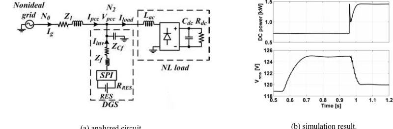
B. DGS voltage support functionality
4
In order to validate the voltage support function, the capacitor bank, RL load and ܼଶ
5
impedance have been disconnected from the circuit of Fig. 2.a, resulting in the simplified circuit
6
shown in Fig. 4.a, with a voltage drop of about 6% over the line impedance (ܼଵ). Note also from
[image:15.595.179.418.69.400.2]7
Table II that the resulting total line impedance has a reactance to resistance ratio of ten,
8
confirming the inductive nature of the connection. This extreme condition emulates a weak
9
power grid. The RES considered here is a photovoltaic modular string with a boost DC-DC
10
converter.
11
From Fig. 4.b, before activating the voltage support function, the PCC voltage is 119V. After
12
activating the voltage support (0.55s), the PCC voltage is increased to 125V, which corresponds
13
is not using its full capacity to inject active power to the grid. When the available energy
1
increases on the RES side (0.96s), the voltage support function must be inhibited in order to
2
respect the converter limits without reducing the active power injection. It can be observed that
3
the resulting PCC voltage is slightly higher than the initial value, since the voltage drop is
4
decreased by means of the bigger RES active power injection.
5
Note that the spike in the DC power is a consequence of the dynamics of the chosen
6
maximum power point tracking (MPPT) technique in response to an irradiation step. The
7
simulation result has been generated using Beta MPPT technique [27].
8
[image:16.595.76.476.274.406.2](a) analyzed circuit. (b) simulation result.
Fig. 4. Analyzed circuit and simulation result for the voltage support functionality. 9
C. DGS selective compensation capability
10
Five different conditions have been simulated in order to validate the selective compensation
11
capability of the proposed controller. For these results theRREShas been disconnected from the 12
circuit in Fig. 2.a and an additional load Rac has been connected to the circuit to increase the 13
active power demand, as shown in Fig. 5. Fig. 6 and Table IV shows the results for the DGS
14
operating as a selective active power filter, by means of the proposed CPT current
15
decompositions.
16
[image:16.595.207.401.615.737.2]17
Non-Compensation (NC) means that the DGS is only injecting active power (about 600W).
1
The inverter current is based on sinusoidal injection, since from previous discussions it was
2
concluded to be the best option for injecting active power (SCI). In each of the other
3
compensation conditions (݅,݅and݅௩), besides the active power injection (݅∗,݅ௗ∗ ), the DGS
4
runs as active compensator, using different current reference (்݅∗ ).
5
In the last interval the system operates under 30% of voltage sag at the grid side for about five
6
cycles, showing the ride-through capability of the proposed control. Note that the grid voltage is
7
quite distorted during all the simulation, with a THD at the PCC equal to 6.6%, which doesn’t
8
affect the proposed control scheme.
9
[image:17.595.61.511.298.537.2]10
Fig. 6. Simulation result of the DGS acting as a selective compensator: PCC voltage (dashed); load, inverter and grid currents. 11
TABLE IV. CPTPOWER TERMS,VOLTAGE AND CURRENTS ACCORDING TO DIFFERENT CONTROL STRATEGIES. 12
Load NC (ia) ina ir iv
A [kVA] 1.92 1.48 1.08 1.25 1.34
P [kW] 1.62 1.05 1.08 1.08 1.05
Q [kVAr] 0.82 0.83 0.00 0.00 0.83
D [kVA] 0.61 0.62 0.05 0.62 0.05
λ 0.844 0.710 1.00 0.864 0.783
Vpcc[V]
THD [%] 126.98
6.92
127.02
6.98
127.19
6.65
127.18
6.98
126.99
6.63
[image:17.595.192.403.571.764.2]Iinv[A]
THD [%]
---4.65
2.42 9.19
60.4 7.81
2.30 6.67
103.60
1
Observe that in the non-active current (݅) compensation the grid current assumes the same
2
waveform of the PCC voltage, being the RLS the best compensation strategy.
3
In Table IV, except for the “Load” column, all the power values refer to the PCC. Note that
4
the difference between the load active power and the PCC active power corresponds to the
5
power from the RES (about 600W). Moreover, since the CPT current components are
6
completely decoupled (orthogonal), depending on the choice of the current reference, each
7
power quality disturbing effect can be selectively compensated, as indicated by the power
8
components in Table IV. Note that injecting active power into the grid decreases the global
9
power factor (ߣ), because from the PCC point of view only the active power is reduced, whereas
10
the reactive and void powers remain the same. This highlights the importance of the load current
11
compensation performed by the DGS.
12
From the columnsNC(݅)and݅, where the݅௩is sinusoidal (SCI), it is possible to verify the
13
steady state performance of the output current controller [ܥ(ݏ)] and the effectiveness of the
14
output LC filter by means of the inverter current THD, which is 2.4%.
15
VI. EXPERIMENTAL RESULTS 16
The experimental setup is based on the control scheme and circuits of Fig. 1 and Fig. 2.a
17
(refer to Table II for the values of the impedances). The DC-AC conversion stage is a full bridge
18
inverter, with IGBT modules (SKM 75GB128D, driven by SKHI 23/12 – both from Semikron).
19
The voltage and current Hall-effect sensors are from LEM and the control board is a Texas
20
Instruments TMS320F2812. The sampling and switching frequency is set 12 kHz. TheNL load
21
is an uncontrolled rectifier with capacitive filter, representing a usual example of nonlinear load
22
in low voltage distribution systems [28]. A picture of the experimental set-up is shown in Fig. 7.
23
24
25
(a) front view (b) back view
Fig. 7. Picture of the experimental prototype. 1
A. Resistive current versus sinusoidal current for active power injection and current disturbances
2
compensation
3
This section investigates the experimental results anticipated in Table III (in section V-A)
4
regarding to the management of the active power.
5
Fig. 8 shows the grid {4} and PCC {3} voltages, as well as the currents through ܼଵ{1} and
6
ܼଶ{2} line impedances, without the DGS. It is possible to observe that the PCC voltage is quite 7
distorted by the combined effect of the nonlinear load and the resonance, since the grid voltage
8
has 0.4% of the eleventh harmonic order. Table V shows the grid and PCC voltages harmonic
9
spectra, whereas the RMS values and THDs for the grid and PCC voltages are, respectively:
10
119.3V (3.3%) and 116.6V (9.42%).
11
In order to analyze the DGS damping capability against induced resonances, three conditions
12
are tested in Fig. 9 (a-f) and discussed by means of the resulting PCC voltage and ܼଶ current
13
(refer to table III for the exact measurements).
14
Figs. 9.a and 9.b show the DGS running as an APF with SSC and RLS compensation
15
strategies, respectively. As emphasized in section IV-C, the RLS provides more damping effect
16
Figs. 9.c and 9.d show the DGS compensating the load current disturbance by RLS strategy
1
and at the same time injecting about 800W of active power into the grid by SCI (Fig. 9.c) and
2
RCI (Fig. 9.d). The PCC voltage in Fig. 9.c (SCI) is slightly less distorted than the Fig. 9.d
3
(RCI).Z2current is very small due to the DGS is compensating all the load current disturbances 4
and providing the main portion of the active power to the load.
5
[image:20.595.54.528.53.644.2]6
Fig. 8. Grid and PCC voltages andZ1andZ2line impedance currents - circuit without DGS. 7
TABLE V. GRID ANDPCCVOLTAGE SPECTRA. 8
Harm. 3° 5° 7° 9° 11° 13° 15°
Vgrid[%] 1.8 2.3 1.4 0.2 0.4 0.1 0.1
VPCC[%] 7.4 4.5 2.6 1.9 1.7 0.7 0.3
9
[image:20.595.214.382.198.331.2](c) RLS strategy and SCI strategy. (d) RLS strategy and RCI strategy.
[image:21.595.93.497.69.390.2](e) SSC strategy and SCA strategy. (f) SSC strategy and RCA strategy.
Fig. 9. Resistive current versus sinusoidal current for active power injection and current disturbances compensation. 1
Fig. 9.e and 9.f show the DGS compensating the load current disturbance by SSC strategy and
2
absorbing about 800W of active power from the grid by SCA and RCA , respectively. In this
3
case theRREShas been connected to the DC link. From the PCC voltage point of view, it can be 4
clearly observed that the active power absorption by RCA (Fig. 9.f) is better than the SCA (Fig.
5
9.e). All these results support the conclusions of section IV-A.
6
B. DGS selective compensation capability
7
Finally, Figs. 10 depict some experimental results of the DGS acting as an active
8
compensator. The system used here is the same used for the simulations in section V-C,
9
changing theZ1impedance, which is now the real grid line impedance with unknown value. 10
The local load has a power factor equal to 0.87 and current THD equal to 33%. Each Fig.
(a-11
d) reports the PCC voltage {4} and current terms (inverter {1}, grid {2} and load {3}) using
12
different current references.
13
Fig. 10.b shows that after compensation (RLS), the grid provides only part of the load active
total harmonic distortion (about 5.5%). Based on Table III, if we had used SSC compensation
1
the inverter current should be practically sinusoidal, whereas the PCC voltage THD should be
2
higher.
3
In this case, the inverter is set to inject about 50% of the load active power demand, as well as
4
to provide non-active current compensation using (4). Note that 3.3% of the current THD comes
5
from the distorted grid voltage, since RLS compensation strategy has been used. The sinusoidal
6
active current injection (SCI), from Fig. 10.a, has about 2.5% of THD, which is due to the
7
current controller.
8
In addition, Figs. 10.c and 10.d show the DGS injecting active power and simultaneously
9
compensating only the reactive and void power, respectively.
10
(a) active power injection. (b) active power injection andinacompensation.
[image:22.595.65.495.276.704.2](c) active power injection andircompensation. (d) active power injection andivcompensation.
Fig. 10. DGS providing active power from the RES and selective power quality compensation. 11
To analyze the selective compensation under load steps, Fig. 11 shows a raise of 40% on the
12
load demand obtained by switching Rac on. Fig. 11.a and Fig. 11.b show, respectively, the 13
reactive and void selective compensation under the step disturbance, occurring in
correspondence to the center of the visualized time interval. It can be observed that the system
1
respond quite satisfactorily to external disturbances.
2
[image:23.595.68.504.96.288.2](a) active power injection andircompensation. (b) active power injection andivcompensation.
Fig. 11. DGS providing active power from the RES and selective compensation – dynamic response for load changing. 3
VII. CONCLUSIONS 4
This paper proposes a multi-task control strategy for distributed generation systems. The main
5
functionalities are based on the CPT definitions, which gives flexibility to the system, especially
6
when the instantaneous inverter capability is limited. As demonstrated, in addition to the active
7
power injection, the proposed methodology allows voltage level regulation or selective load
8
current disturbances mitigation. Note that the control strategies do not use any kind of
9
reference-frame transformation and it can be applied without any additional consideration, even
10
if the PCC voltage is non-sinusoidal.
11
It has also been shown that the best method to inject active power to the grid is using a
12
sinusoidal current reference, as it avoids the amplification of possible resonances in the system.
13
Conversely, in order to absorb active power from the grid, e.g. to charge a battery bank or to
14
operate the inverter as a controlled rectifier, it is suggested to use a resistive current reference, to
15
increase the damping effect on the PCC, minimizing possible resonant conditions.
16
ACKNOWLEDGMENT 17
The authors are grateful to FAPESP (proc. 2012/24309-8, 2012/14014-0 and 2013/08545-6),
18
Fundunesp and CNPq (proc. 487471/2012-1 and 554960/2006-0) for the support provided to
19
this research.
REFERENCES 1
[1] Mozina, C. J.: ‘Impact of smart grids and green power generation on distribution systems’, IEEE
2
Trans. on Industry Applications, 2013, 49, (3), pp. 1079-1090.
3
[2] International Energy Outlook 2013: ‘U.S. Energy Information Administration (EIA)’,
4
http://www.eia.gov/forecasts/aeo/, accessed April 2014.
5
[3] Carnieletto, R., Brandão, D. I., Farret, F. A.,et al.: ‘Smart grid initiative’, IEEE Trans. on Industry
6
Applications Magazine, 2011, 17, (5), pp. 27-35.
7
[4] Macken, K. J. P., Bollen, M. H. J., Belmans R. J. M.: ‘Cost-effectiveness of distributed power quality
8
compensation’, IEEE Power Engineering Society General Meeting, 2003, pp. 1130-1135.
9
[5] Bidram, A., Davoudi, A., Lewis, F. L., Zhihua Qu: ‘Secondary control of microgrids based on
10
distributed cooperative control of multi-agent systems’, IET Generation, Transmission & Distribution,
11
2013, 7, (8), pp. 822–831.
12
[6] Jinwei He, Yun Wei Li, Blaabjerg, F.,et al.: ‘Active harmonic filtering using current-controlled,
grid-13
connected DG units with closed-loop power control’, IEEE Trans. on Power Electronics, 2014, 29, (2),
14
pp. 642-653.
15
[7] Jinwei He, Yun Wei Li, Munir, M. S.: ‘A flexible harmonic control approach through
voltage-16
controlled DG-grid interfacing converters’, IEEE Trans. on Industrial Electronics, 2012, 59, (1), pp.
444-17
455.
18
[8] Wang, F., Duarte, J. L., Hendrix, M. A. M.: ‘Design and analysis of active strategies for distributed
19
generation inverters under unbalanced grid faults’, IET Generation, Transmission & Distribution, 2010, 4,
20
(8), pp. 905-916.
21
[9] Bojoi, R., Limongi, L. R., Roiu, D.,et al.: ‘Enhanced power quality control strategy for single-phase
22
inverters in distributed generation systems’, IEEE Trans. on Power Electronics, 2011, 26, (3), pp.
798-23
806.
24
[10] Maza-Ortega, J. M., Gómez-Expósito, A., Barragán-Villarejo, M.,et al.: ‘Voltage source
converter-25
based topologies to further integrate renewable energy source in distributed systems’, IET Renewable
26
Power Generation, 2012, 6, (6), pp. 435-445.
27
[11] Ortjohann, E., et al.: ‘A general architecture for modular smart inverters’, IEEE International
28
Symposium on Industrial Electronics, 2008, pp. 1525-1530.
[12] Kroposki, B., Pink, C., De Blasio, R.,et al,: ‘Benefits of power electronic interfaces for distributed
1
energy systems’, IEEE Trans. on Energy Conversion, 2010, 25, (3), pp.901-908.
2
[13] Tenti, P., Costabeber, A., Mattavelli, P.,et al,: ‘Distribution loss minimization by token ring control
3
of power electronic interfaces in residential microgrids’, IEEE Trans. on Industrial Electronics, 2012, 59,
4
(10), pp. 3817-3826.
5
[14] Tenti, P., Costabeber, A., Mattavelli, P.: ‘Improving power quality and distribution efficiency in
6
micro-grids by cooperative control of switching power interfaces’, International Power Electronics
7
Conference, 2010, pp. 472-479.
8
[15] Tenti, P., Paredes, H. K. M., Mattavelli, P.: ‘Conservative power theory, a framework to approach
9
control and accountability issues in smart microgrids’, IEEE Trans. on Power Electronics, 2011, 26, (3),
10
pp. 664-673.
11
[16] Marafão, F. P., Brandão, D. I., Gonçalves F. A. S., Paredes, H. K. M.: ‘Decoupled reference
12
generator for shunt active filter using the Conservative Power Theory’, Journal of Control, Automation
13
and Electrical Systems, 2013, 24, pp. 522-534.
14
[17] Paredes, H K M.: ‘Conservative Power Theory: a new approach to cooperative control of power
15
conditioners and considerations regarding to responsibility assignment’. PhD thesis, State University of
16
Campinas, 2011, (in Portuguese).
17
[18] Zuniga, T. E. N., Pomilio J. A.: ‘Shunt active power filter synthesizing resistive load’, IEEE Trans.
18
on Power Electronics, 2002, 16, (2), pp. 273-278.
19
[19] Marafão F. P., Deckmann, S. M., Pomilio, J. A., Machado, R. Q.: ‘Selective disturbance
20
compensation and comparison of active filtering strategies’, IEEE International Conference on Harmonics
21
and Quality of Power, 2002, pp. 484-489.
22
[20] Bollen, M. H. J., Sannino A.: ‘Voltage control with inverter-based distributed generation’ IEEE
23
Trans. on Power Delivery, 2005, 20, (1), pp. 519-520.
24
[21] Brandão, D. I., Marafão, F. P., Simões, M. G., Pomilio, J. A.: ‘Considerations on the modeling and
25
control scheme of grid connected inverter with voltage support capability’, Brazilian Power Electronics
26
Conference, 2013.
27
[22] K. Ogata: ‘Modern control engineering’ (Prentice Hall, 2010, 5th edn).
28
[23] Mattavelli, P., Buso, S.: ‘Digital control in power electronics’ (Morgan & Claypoo, 2006, 1st edn).
[24] Chen, Z., Blaabjerg, F., Pedersen, J. K.: ‘Harmonic resonance damping with a hybrid compensation
1
system in power systems with dispersed generation’ IEEE Power Electronics Specialist Conference,
2
2004, pp. 3070-3076.
3
[25] Fujita, H a., Akagi, H.: ‘A practical approach to harmonic compensation in power systems-series
4
connection of passive and active filters’, IEEE Trans. on Industry Applications, 1991, 27, (6), pp.
1020-5
1025.
6
[26] Wada, K., Fujita, H., Akagi, H.: ‘Considerations of a shunt active filter based on voltage detection
7
for installation on a long distribution feeder’, IEEE Trans. on Industry Applications, 2002, 38, (4), pp.
8
1123-1130.
9
[27] Canesin, C. A., Brito, M. A. G., Sampaio, L. P.,et al.: ‘Evaluation of main MPPT techniques for
10
photovoltaic applications’, IEEE Trans. on Industrial Electronics, 2013, 60, (3), pp. 1156-1167, 2013.
11
[28] Pomilio, J. A., Deckmann, S. M.: ‘Characterization and compensation of harmonic and reactive
12
power of residential and commercial loads’, IEEE Trans. on Power Delivery, 2007, 22, (2), pp.
1049-13
1055.