Gridded Parasitic Patch Stacked Microstrip Antenna with Beam
Shift Capability for 60 GHz Band
Alexander Bondarik* and Daniel Sj¨oberg
Abstract—A microstrip antenna design is introduced in which aperture coupled rectangular microstrip patch is coupled electromagnetically with a parasitic gridded rectangular patch placed above. The gridded patch consists of nine identical rectangular parts separated by a distance which is much smaller than a free space wavelength for a central frequency. The antenna is designed to operate in the 60 GHz band and is fabricated on a conventional PTFE (polytetrafluoroethylene) thin substrate. Different published arrangements for parasitic patches are studied. For the same substrate and central frequency the proposed antenna has improved return loss bandwidth and gain bandwidth. Measurement results are in good agreement with simulation. Measured 10 dB return loss bandwidth is from 54 GHz up to 67 GHz. It fully covers the unlicensed band around 60 GHz. The measured antenna realized gain at 60 GHz is close to 8 dB, while the simulated antenna radiation efficiency is 85%. A beam shifting method is proposed for this antenna structure by connecting adjacent outside parts in the gridded patch. The designed antenna is suitable for a high speed wireless communication system in particular for a user terminal in a fifth generation (5G) cellular network.
1. INTRODUCTION
The last decade has seen a heightened interest in the unlicensed frequency band around 60 GHz. Wide, globally available bandwidth and high propagation attenuation allow for numerous applications requiring multi-Gb/s data wireless communication on a short range [1–3].
Antenna is among the critical elements for a wireless system. It should have a wide bandwidth characteristic to take advantage of the 60 GHz frequency band. For a majority of systems a 7 GHz 10 dB return loss bandwidth is specified. However, for a global usage the antenna should be able to operate from 55 GHz up to 67 GHz, i.e., cover 12 GHz bandwidth [2]. To overcome the propagation attenuation the antenna should have a high efficiency and a high gain. The latter specification implies a sharp antenna beam shape and therefore a beam steering is a requirement for some applications. The beam shift technique should preferably be simple and cost-effective [3]. Another important issue is antenna robustness and ease of integration with other components inside a wireless system. It means that the antenna should be compact and fabricated using conventional techniques [4, 295–348]. Antenna packaging techniques have certain restrictions on substrate material and substrate thickness. Usually there exists a limit in substrate height [5]. Some applications require antenna integration in portable terminals and clothing [6], therefore antenna should be conformal and flexible, which is much easier to achieve with thin substrate.
One of the possible solutions is a patch antenna. However, a classical design with a single metal patch above a ground plane cannot satisfy the bandwidth requirement, and additional techniques need to be used to enlarge this characteristic. Microstrip antenna structures with multiple resonances have been proven to increase operational bandwidth and antenna gain significantly. Designs for 60 GHz are reported in several papers. An aperture coupled patch antenna is described in [7]. The antenna uses
Received 23 January 2015, Accepted 8 April 2015, Scheduled 6 May 2015 * Corresponding author: Alexander Bondarik ([email protected]).
an aperture and a patch as two coupled resonators. As a result, 7 GHz bandwidth and 7 dB gain at 60 GHz have been achieved. In [8] a parasitic patch is placed above a probe-fed microstrip patch. The combination of two coupled patches gives about 9 GHz bandwidth and about 5 dB gain at 60 GHz. An aperture coupled two patches stacked design is presented in [9]. The features for this antenna are a differential feeding scheme and an H-shape aperture. Reported return loss bandwidth is from 50 GHz to 78 GHz, but the antenna gain has significant drops inside the mentioned band. A microstrip antenna stacked design is presented in [10]. The antenna consists of a probe fed patch and two layers of parasitic patches, four patches in each layer. Due to the large radiating aperture, the antenna has a large gain, 11 dB. The return loss bandwidth is about 2 GHz. In [11] an aperture coupled stacked microstrip antenna has four parasitic patches on a top layer. A simulation shows 10 GHz bandwidth and 6 dB gain at 60 GHz; however there is no measurement provided.
In the current paper, a novel aperture coupled microstrip antenna stacked design is proposed. The traditional design introduced in [12] and further investigated carefully in [13–16] is modified using a gridded structure for the parasitic microstrip patch, instead of a single parasitic patch. The parasitic patch design concept is similar to the gap-coupled rectangular microstrip antennas reported in [17, 18] and [19, 171–203]. The antenna proposed in this paper has nine parasitic patches arranged in a grid and aperture coupling feeding, whereas five parasitic patches and probe feeding were used in [19, 171–203]. We explain a design procedure, and make a detailed comparison between our concept and three similar concepts. The first uses a single parasitic patch. The second was first introduced in [20] and implemented at 60 GHz in [11], it uses four parasitic patches. The third concept uses five gap-coupled patches. All four antenna concepts are optimized at 60 GHz central frequency to maximize 10 dB return loss. It is shown that the gridded parasitic patch antenna has the widest return loss bandwidth. Moreover, the gridded structure of the parasitic patch can be used for a beam shift realization by implementing shorting elements or capacitive loadings. The antenna has high simulated efficiency. The fabrication is relatively simple and uses standard commercial processes. Measurement results are in good agreement with simulation. The gridded parasitic patch antenna can be used in a 5G network user terminal where a small thickness, high directivity and beamforming are an issue [21].
The main contributions of the paper are a novel antenna design for 60 GHz band and a beam shift method for the proposed antenna. The antenna structure is a previously unreported development of existing antenna concepts. It is shown that the proposed antenna has improved return loss and gain compared to antenna structures in related publications. Moreover, the provided antenna comparison is a good guidance for practical mm-wave antenna designs. An antenna with five gap-coupled parasitic patches is considered for the first time with aperture coupling feeding.
The paper is organized as follows. The structure of the gridded parasitic patch stacked microstrip antenna is presented in Section 2. In Section 3 alternative antenna designs and their detailed comparison are described. Section 4 contains the parameter study for the proposed antenna. Fabricated antenna sample parameters are presented in Section 5. Simulated and measured results of the test structure are presented in Section 6. A beam shift realization is presented in Section 7. Conclusions are made in Section 8.
2. ANTENNA STRUCTURE
The proposed antenna geometry is shown in Figure 1. In Table 1 the antenna substrate and feeding line parameters are listed. A PTFE (polytetrafluoroethylene) substrate and a bonding film are used
Table 1. Stacked microstrip antenna design parameters.
Description Value
substrate Taconic TLY-5 r= 2.2, tanδ= 0.0009 parasitic substrate thickness,h 0.127 mm
microstrip substrate thickness 0.127 mm bonding film Arlon CuClad 6700 r= 2.35, tanδ= 0.0025
Gridded parasitic patch
Feeding patch Parasitic substrate
Bonding film
Slot
Ground plane
Microstrip substrate
Microstrip line Lp
d
Lf Wp
Wf
x
y z
Figure 1. Geometry of the aperture coupled stacked microstrip antenna with gridded parasitic patch.
Figure 2. Simulated reflection coefficient of the single parasitic patch antenna, four para-sitic patches antenna, five gap-coupled parapara-sitic patches antenna, and gridded parasitic patch an-tenna. Design parameters are in Table 2.
to form a three-layer structure. The permittivity for both materials has close values. The fabrication procedure is conventional. On the bottom there is a 50 Ω microstrip line that feeds a single rectangular patch (“feeding patch”) using aperture coupling through a slot in the ground plane. The bonding film acts as a substrate for the feeding patch. The thickness of the bonding film is small, compared to the substrate thickness, and ensures a strong coupling to the microstrip line. The total antenna substrate thickness is 0.33 mm, which is 0.066λ0 expressed in the free space wavelength at 60 GHz. The substrate thickness above a ground plane is 0.04λ0.
On the top, there is a gridded parasitic patch formed by nine identical rectangular parts. The gridded patch is coupled electromagnetically to the feeding patch. The separation between the rectangular parts in the gridded patch is much smaller than a rectangular parts size. The idea is to keep a strong coupling between different parts. Aperture coupling in the ground plane allows exciting the feed patch symmetrically. The latter feature influences radiation pattern symmetry.
3. ANTENNA COMPARISON
In this section we make a detailed comparison of the proposed antenna to published antenna structures. Four antennas are designed at 60 GHz central frequency and using CST Microwave Studio software they are optimized to have maximum 10 dB return loss bandwidth for given substrate structure and feeding line width.
In particular, it is important to weigh the gridded parasitic patch to the well-studied and widely used single parasitic patch. In [15], 69% measured 10 dB return loss bandwidth is reported. To achieve such a wide bandwidth, a combination of moderate (r = 2.2) and low (r = 1.07) dielectric constant substrates are used. Moreover, a superstrate layer (r = 2.53) is used. The total substrate thickness above a ground plane is 0.2λ0 for 7 GHz central frequency. For 60 GHz central frequency, the scaled substrate thickness is 1 mm, and it can be a considerable fraction of thickness for a user terminal, like a mobile phone with less than 10 mm thickness.
maximum gain and radiation efficiency (dashed lines). Even though the single parasitic patch antenna has acceptable return loss characteristic, it is considered as impractical due to the big ratio between radiating patch width and length, which is 3.5. The common suggestion is to keep the ratio less than 2 in order to avoid additional mode excitation [22]. This means that it is not possible to design a reliable aperture coupled single parasitic patch antenna for the chosen substrate. It has been noticed that the way to keep the parasitic patch width comparable to length is to increase the parasitic substrate thickness.
The other way to match the single parasitic patch antenna on a substrate of given thickness is to add additional parasitic patches close to the main patch on the antenna top layer. Four parasitic patches arrangement is introduced in [20] and discussed in [19, 171–203]. Figure 2 shows simulated reflection coefficient for the four parasitic patches antenna, and Figure 3 shows simulated maximum gain and radiation efficiency. In Table 2, the antenna design parameters are listed.
An alternative parasitic layer design is to use closely coupled patches. This approach is introduced in [17, 18]. In case when four parasitic patches are placed along to a single patch sides, the parasitic patches geometry forms a structure similar to a plus sign. A stacked antenna structure with this parasitic patches arrangement is studied in [19, 171–203], where a probe feeding is used. However, we have not found a previous use of an aperture coupling feeding for this antenna structure. Figure 2 shows simulated reflection coefficient for the five parasitic patches antenna, and Figure 3 shows simulated maximum gain and radiation efficiency. In Table 2, the antenna design parameters are listed.
The natural development for the five parasitic patches antenna would be to add four more parasitic patches forming a gridded structure. This design does not require additional increase in antenna aperture length and width. By doing this we introduce a novel aperture coupled stacked microstrip antenna with gridded patch. The design parameters for this antenna are presented in Table 2. The simulated reflection coefficient is shown in Figure 2, and Figure 3 shows simulated maximum gain and radiation efficiency (solid lines).
Table 2. Design parameters for antenna comparison.
Parameter Single parasitic Four parasitic Five parasitic Gridded patch microstrip line stub,S 0.56 mm 0.51 mm 0.42 mm 0.72 mm
slot length,Ls 0.18 mm 0.18 mm 0.25 mm 0.27 mm slot width,Ws 0.90 mm 0.89 mm 1.03 mm 1.07 mm
feeding patch length,Lf 1.21 mm 1.04 mm 0.80 mm 1.15 mm
feeding patch width,Wf 1.38 mm 1.19 mm 1.58 mm 1.89 mm parasitic patch length,Lp 1.40 mm 1.36 mm 1.24 mm 1.11 mm parasitic patch width,Wp 4.90 mm 1.28 mm 1.62 mm 1.03 mm
parasitic patches separation,d 0.75 mm 0.10 mm 0.06 mm
Comparing the reflection coefficient one can notice that the single parasitic patch antenna has the lowest impedance bandwidth. Bandwidth increases for the four parasitic patches antenna and for the five gap-coupled parasitic patches antenna. At 60 GHz, four parasitic patches antenna gain is higher than five gap-coupled parasitic patches antenna gain which in turn is higher than single parasitic patch antenna gain. This agrees well with the antenna comparison provided in [19, Page 183, Page 188]. The gridded parasitic patch antenna has the widest 10 dB return loss bandwidth. Although maximum gain is close to four parasitic patches antenna maximum gain, gain bandwidth for gridded parasitic patch antenna is much wider as can be seen from Figure 3. Radiation efficiency for the five gap-coupled parasitic patches antenna and for the gridded parasitic patch antenna is approximately the same at 60 GHz, about 95%. The four parasitic patches antenna and single parasitic patch antenna efficiency is about 93% at 60 GHz.
Figure 4 shows a comparison for simulated absolute value of the electric field distribution at 60 GHz at the top surface of different antennas. In the four parasitic patches antenna field has equal amplitude on all top patches. Moreover, the phase of excitation is the same. In contrast, in the five gap-coupled parasitic patches antenna and in the gridded parasitic patch antenna, the phase of the field on the top layer central patch is different from the phase of the outer patches due to the capacitive coupling to the central patch. This explains the fact that the four parasitic patches antenna has the highest gain at 60 GHz. In five gap-coupled parasitic patches antenna, two out of five patches have weak amplitude field excitation. The induced field on the additional patches in the gridded parasitic patch antenna adds to the antenna gain compared to the five gap-coupled parasitic patches antenna, which enables higher gain with smaller antenna aperture. At 60 GHz the single parasitic patch antenna has gain comparable to the five gap-coupled parasitic patches antenna; however, the single parasitic patch antenna has considerably wider aperture.
A summary for antennas comparison is provided in Table 3. To conclude, the proposed aperture coupled gridded parasitic patch stacked microstrip antenna structure has considerably improved return loss characteristic compared to similar considered stacked microstrip antenna configurations. For the operational band, the proposed antenna gain is higher than that for the five gap-coupled parasitic patches antenna and the single parasitic patch antenna, in spite of smaller aperture. The gain of the four parasitic patches antenna is higher, but its gain bandwidth is more narrow than the proposed antenna.
Figure 4. Simulated absolute value of the electric field distribution at 60 GHz at the top surface of single parasitic patch antenna, four parasitic patches antenna, five gap-coupled parasitic patches antenna, and gridded parasitic patch antenna.
Table 3. Antenna parameters comparison.
Parameter Single parasitic Four parasitic Five parasitic Gridded patch 10 dB return loss bandwidth 11.3 GHz 12.4 GHz 14.9 GHz 17.0 GHz
4. PARAMETER STUDY
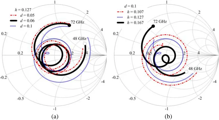
All the parameters listed in Table 1 and Table 2 affect the antenna characteristics. The variation in slot size, feeding patch size, parasitic patch size, and substrate thickness between ground and feeding patch has similar effect as for the aperture coupled stacked antenna with single parasitic patch, which is carefully investigated in [13, 15]. In this section a parameter study for the gridded parasitic patch antenna is focused on the influence of the separationdbetween adjacent parasitic patches in the grid and substrate thicknesshbetween the feeding patch and parasitic patches. Figure 5(a) shows the simulation result for different separation values. The frequency variation is from 48 GHz to 72 GHz. The optimized separation is d = 0.06 mm, and the variation from this value results in impedance mismatch. The effect is in the changed coupling between feeding and gridded patch which greatly changes one of the two loops typical for three resonances aperture coupled stacked structure. The mutual resonance between the ground plane aperture and lower patch is associated with the lower frequency loop, and the mutual resonance of the feeding patch and parasitic patches is associated with the upper frequency loop [15]. The parasitic patches resonance behavior can be modelled as a resonator with equivalent impedance. Based on this model, the mismatch presented in Figure 5(a) can be explained by change in the equivalent reactance when the distance between parasitic patches is changed. Indeed, the impedance loci turn counterclockwise when decreasing the equivalent reactance by decreasing separationdand turn clockwise when increasing the equivalent reactance by increasing separation d.
The antenna impedance mismatch due to the change in separationdcan be partially compensated by changing the substrate thickness h between the feeding patch and parasitic patches. Figure 5(b) shows the simulation result for increasedd. As can be seen from the chart, when increasing the substrate thicknessh, the high frequency loop becomes larger, with increasing coupling between the feeding patch and parasitic patches. In the same time, the low frequency loop becomes smaller and fits inside the 10 dB return loss circle. On the contrary, when the substrate thicknesshis decreased, the high frequency loop becomes smaller, and the low frequency loop becomes larger, and for d = 0.10 mm this leads to the antenna mismatch. Since for d= 0.05 mm two impedance loops are already large, a change in the substrate thickness h will lead to antenna mismatch. In order to match the antenna in this case, the other antenna parameters need to be changed in combination with substrate thicknessh.
The parametric study shows that the gridded parasitic patch antenna gain is higher for decreased
d, since the electromagnetic coupling between separated patches in the grid becomes stronger. In the
(a) (b)
substrate thickness h variation the antenna gain increases for increased h. This can be explained by the fact that when h is increased, the coupling of the feeding patch and the outer parts in the grid structure increases as well. For the accomplished parametric study the antenna normalized radiation pattern undergos just slight changes.
5. ANTENNA EXPERIMENTAL VERIFICATION
To verify the gridded parasitic patch antenna performance, a prototype was fabricated. The fabricated antenna sample with connector is shown in Figure 6. In Table 4 the antenna design parameters are listed, and they are slightly different from those presented in Table 2. For the fabricated antenna sample, the return loss optimization goal was set to 20 dB for frequencies 57 GHz–63 GHz. This was done in order to have a margin and to mitigate the mismatch losses for the antenna design with beam shift. The other reason was to comply with design rules for the antenna fabrication process by setting the distance between adjacent patches in the grid tod= 0.10 mm.
To be able to attach the connector the fabricated antenna samples substrate was made large enough. The sample size was 40 mm by 20 mm. A part of the substrate close to the connector was removed to expose the ground plane and ensure a good contact for the connector. The remaining substrate size is 20 mm by 20 mm.
y x
Figure 6. Front and backside photographs of the fabricated antenna with end launch connector.
Parameter Value microstrip line stub,S 0.50 mm
slot length, Ls 0.20 mm slot width,Ws 0.85 mm feeding patch length,Lf 1.10 mm feeding patch width, Wf 1.29 mm parasitic patch length, Lp 1.16 mm parasitic patch width,Wp 1.20 mm parasitic patches separation, d 0.10 mm
Table 4. Gridded parasitic patch antenna fabricated sample parameters.
6. MEASUREMENT RESULTS
The aperture coupled gridded parasitic patch stacked microstrip antenna parameters were measured using a 67 GHz Agilent E836A PNA network analyzer. The antenna was fed through a 1.85 mm end launch connector from Southwest Microwave company. To validate the antenna measurements a 3D connector model was developed in CST. Moreover, the microstrip line area in touch with the connector was optimized to have a tapered form, and it has metal pads at both sides to be matched to the connector and to have a good contact with the connector body. The following measurement results are compared to a simulation including the antenna and the connector as a single system. To investigate the connector influence, simulated results for the antenna without connector are presented as well. The antenna radiation patterns and gain measurements were performed in a regular empty office room, the approximate room size was 10 m by 7 m by 2.5 m.
6.1. Reflection Coefficient
Figure 7. Measured and simulated reflection coefficients of the antenna.
results for the antenna with and without connector. This confirms the connector reliability and small influence on the antenna return loss.
6.2. Radiation Patterns
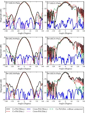
Measured and simulated normalized radiation patterns for 57 GHz, 60 GHz, and 64 GHz are shown in Figure 8. Co-polarization and cross-polarization components in H-plane (yz plane) and E-plane (xz
plane) are presented. In the E-plane, the simulated cross-polarization level is out of the scale for the graphs. For comparison, simulated results for the antenna without connector are presented. Measured patterns are close to simulated ones. For the main beam, in the range between −90◦ and 90◦, the patterns are almost coinciding. Small differences are observed for the antenna back radiation.
The measuredH-plane patterns have different levels for the back radiation for negative and positive angles due to the fact that the setup itself is not symmetrical. There was a network analyzer on one of the sides, and the distances to the walls were not identical. However, the measured maximum back radiation level at±180◦ for 60 GHz and 64 GHz coincides with simulation within 2 dB, for 57 GHz the measured level is lower, this might be the measurement error. Measured results are in better agreement with the simulation that includes connector. This gives reason to state that for the antenna itself, without the connector influence, the back radiation level is close to the simulated results without connector, which is about−20 dB for 57 GHz and 60 GHz. For 64 GHz, the level is close to−30 dB. The measured cross-polarization component is less than−25 dB for considered frequencies.
The E-plane co-polarization radiation patterns have wider asymmetrical main beam than theH -plane patterns, and the patterns have ripples for all angles. The measured cross-polarization level is about −30 dB for the frequencies presented in Figure 8. For the gridded parasitic patch antenna there is an explicit local peak in theE-plane at the angles from about 90◦ to 110◦. This peak disappears in the simulation without connector.
Moreover, the back radiation level for this simulation is about 10 dB lower than the measured pattern. The explanation for the described effect is the presence of radiation along the substrate (xy
plane). Figure 9 shows the simulated top surface electric field distribution for the antenna without the connector. The wave reflected from the connector causes the mentioned local peak around 90◦. It can be observed from Figure 9 that the radiation along the substrate is symmetrical with respect to xz
Figure 8. Measured and simulated normalized radiation patterns in the H-plane and in the E-plane of the antenna with end launch connector. Co-polarization and cross-polarization patterns for three frequencies of interest are presented. In theE-plane the simulated cross-polarization level is out of the scale. Simulation results for the antenna without connector are presented as well.
6.3. Gain and Efficiency
The antenna realized gain was measured based on the gain-transfer method [24]. Measured and simulated realized gains are shown in Figure 10. For comparison, the antenna gain when simulated without connector is also shown. The agreement between measurements and simulation is good. All three curves agree within 2 dB in the frequency range from 57 GHz up to 62 GHz. Maximum measured realized gain is about 9 dB for 66 GHz. At 60 GHz, the antenna has about 8 dB realized gain. However, based on the simulation results, the influence of the connector decreases gain bandwidth, and the antenna itself should have wider bandwidth than measured. In the application when the antenna is integrated with other components some degradation of parameters should be expected.
7. BEAM SHIFT REALIZATION
In this section, two examples of the H-plane beam shift realization for the gridded parasitic patch antenna are described. The purpose of this section is to introduce the beam shift principle and to outline thereby the significance of the proposed antenna. Simulated results are presented. Due to the limited space the detailed investigation of the phenomena and experimental results are out of the scope for the current paper. The proposed beam shift is realized by utilizing the so called ESPAR (Electronically Steerable Parasitic Array Radiator) principle [25]. The ESPAR exhibits a unique phase shifting mechanism where mutual coupling between adjacent radiators feeds the parasitic radiators, and tunable reactive loading at the terminals of the parasitic radiators creates the necessary phase shift [25]. In the first proposed beam shift method, a radiating structure asymmetry is realized by connecting adjacent patches in the grid. In Figure 11(a) shows an example where three patches are connected by shorting metal pins in the xy plane. The shorting pin width is 0.1 mm. Practically this can be accomplished by implementing a switch (either on ground plane side or on top layer side) using PIN diodes or MEMS elements. Then by opening or closing the switch a beam steering can be achieved. The benefit of this method is its simplicity.
y x
Figure 9. Simulated absolute value of the electric field distribution at 60 GHz, at the top surface of the structure.
Figure 10. Measured and simulated realized gains of the antenna with connector are com-pared to the simulated gain of the antenna with-out connector. Radiation efficiency simulation result for the antenna without connector.
0.4 mm Shorting pins
0.1 mm
y x
0.4 mm 1 fF 1 fF
10 fF 10 fF y
x
(a) (b)
Figure 11. Gridded parasitic patch top view geometry enabling the H-plane beam shift. (a) With shorting pins. The pin width is 0.1 mm, distance from the pin center to the patch edge is 0.4 mm. (b) With capacitors. Distance from the capacitor to the patch edge is 0.4 mm.
Figure 13. Simulated radiation patterns at 60 GHz for the antennas with beam shift and for the reference antenna without beam shift.
In the second beam shift method capacitors are used instead of shorting elements. Figure 11(b) shows the antenna radiating layer geometry. Four capacitors with nominal values 1 fF and 10 fF are arranged symmetrically with respect toxzplane. It should be noticed that if all capacitors have nominal values 1 fF or less, they do not introduce any effect on the antenna performance.
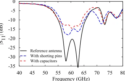
The simulation was performed to check the beam shift capability for the gridded parasitic patch. The ground plane size in the model was 40 mm by 20 mm. Shorting pins and capacitors implementation change the mutual coupling between the feeding patch and the gridded parasitic patch. This results in the antenna and the feeding line impedance mismatch. The antenna return loss for two beam shift methods is shown in Figure 12, and for comparison return loss is presented for the reference antenna without loading elements. The antenna with shorting pins 10 dB return loss bandwidth is 9.2 GHz which is slightly less than the reference antenna. The antenna with capacitors has 8 GHz bandwidth, and it is still suitable for 60 GHz communication systems. A low 20 dB return loss level for the reference antenna provides some safety factor in the geometry modification.
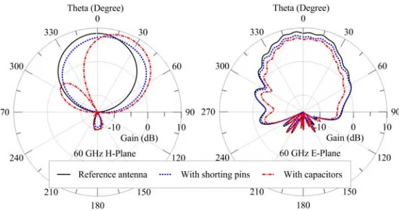
Figure 13 shows simulated gain radiation patterns at 60 GHz for the antenna with shorting pins and with capacitors compared to the reference antenna radiation patterns. In theH-plane the antenna with shorting pins has 10◦ beam shift angle. The maximum gain is 0.8 dB lower than for the reference antenna, and the beam width is 64◦ compared to the 54◦ reference antenna beam width. The antenna with capacitors has 20◦ beam shift angle. The maximum gain is actually 0.4 dB higher than that for the reference antenna, and the beam width is 48◦. Using the same techniques due to the symmetry, it is possible to shift the beam on−10◦ and on−20◦. In theE-plane, there is no beam shift for the antenna with loading elements, and it still has maximum in the broadside direction, like the reference antenna. Although the antenna with shorting pins has some degradation in gain and return loss bandwidth, it is not significant. It confirms that the proposed simple beam shift method is effective. The beam shift realization for the gridded parasitic patch antenna using capacitive loading has essential improvements when compared to realization described in [25] where close coupled patches are considered in a single layer microstrip antenna. The proposed method uses less loading capacitors and still preserves wide return loss bandwidth. Moreover, the proposed method is more suitable for a stacked antenna configuration.
8. CONCLUSIONS
patches. The design target for all the antennas was set to maximize 10 dB return loss bandwidth. It was shown that the single parasitic patch antenna design is impractical for the given substrate due to the very wide parasitic patch. The single parasitic patch antenna, four parasitic patches antenna and five gap-coupled parasitic patches antenna have considerably less impedance bandwidth than the gridded parasitic patch antenna. For the operational band the proposed antenna gain is higher than five gap-coupled parasitic patches antenna and single parasitic patch antenna gain, in spite of smaller aperture. Four parasitic patches antenna gain is higher; however, gain bandwidth is more narrow than the proposed antenna. For the antenna measurements, a connector was used. To validate the measurements, a 3D end launch connector model was developed and the influence of the connector was examined. The measured results are very close to the simulated ones. The antenna has wide return loss bandwidth that fully covers the unlicensed communication band around 60 GHz. The antenna has high efficiency inside the operational band. The gridded structure for the proposed antenna can be used to make a simple and inexpensive beam shift realization by connecting adjacent patches in the grid. In the H-plane beam shift example, the obtained beam shift angle was 10◦ at 60 GHz. Using the same technique, the beam shift in the E-plane can be realized as well. It was shown that in a more complex beam shift realization with the use of capacitive loading elements theH-plane beam shift can be 20◦ at 60 GHz, for 8 GHz impedance bandwidth. Potentially it is possible to build an antenna array placing the proposed antennas such that the separation between edges is the same as in the gridded parasitic structure d= 0.1 mm. For this arrangement the distance between single antennas centers is 0.78λ0. If gridded patches in the array are allowed to overlap between neighbors, the distance between feeding patches is about 0.5λ0. The proposed antenna is suitable for the next generation cellular network equipment.
REFERENCES
1. Schulte, B., M. Peter, R. Felbecker, W. Keusgen, R. Steffen, H. Schumacher, M. Hellfeld, A. Barghouthi, S. Krone, F. Guderian, G. P. Fettweis, and V. Ziegler, “60 GHz WLAN applications and implementation aspects,” International Journal of Microwave and Wireless Technologies, Vol. 3, No. Special Issue 2, 213–221, Apr. 2011.
2. Wells, J., “Faster than fiber: The future of multi-Gb/s wireless,” IEEE Microw. Mag., Vol. 10, No. 3, 104–112, Mar. 2009.
3. Guo, N., R. C. Qiu, S. S. Mo, and K. Takahashi, “60-GHz millimeter-wave radio: Principle, technology, and new results,” EURASIP Journal on Wireless Communications and Networking, Vol. 2007, No. 1, 48–48, 2007.
4. Liu, D., U. Pfeiffer, J. Grzyb, and B. Gaucher, Advanced Millimeter-wave Technologies: Antennas, Packaging and Circuits, John Wiley & Sons, 2009.
5. Li, R., G. DeJean, M. Maeng, K. Lim, S. Pinel, M. M. Tentzeris, and J. Laskar, “Design of compact stacked-patch antennas in LTCC multilayer packaging modules for wireless applications,” IEEE Transactions on Advanced Packaging, Vol. 27, No. 4, 581–589, 2004.
6. Chahat, N., M. Zhadobov, and R. Sauleau, “Wearable textile patch antenna for BAN at 60 GHz,” 2013 7th European Conference on Antennas and Propagation (EuCAP), 217–219, IEEE, 2013. 7. Lamminen, A. E. I., J. Saily, and A. R. Vimpari, “60-GHz patch antennas and arrays on LTCC
with embedded-cavity substrates,” IEEE Transactions on Antennas and Propagation, Vol. 56, No. 9, 2865–2874, 2008.
8. Hong, W., A. Goudelev, K.-H. Baek, V. Arkhipenkov, and J. Lee, “24-element antenna-in-package for stationary 60-GHz communication scenarios,” IEEE Antennas and Wireless Propagation Letters, Vol. 10, 738–741, 2011.
9. Yang, B., A. Yarovoy, and S. E. Amaldoss, “Performance analysis of a novel LTCC UWB 60 GHz semi-shielded aperture stacked patch antenna with differential feeding,” Proceedings of the 5th European Conference on Antennas and Propagation (EUCAP), 1882–1885, IEEE, 2011,
11. Bondarik, A., D. S. Jun, J. M. Kim, and J. H. Yun, “Investigation of microstrip antenna array stacked structure realized on LTCC for 60 GHz band,”Microwave and Optical Technology Letters, Vol. 52, No. 3, 648–652, 2010.
12. Tsao, C. H., Y. M. Hwang, F. Kilburg, and F. Dietrich, “Aperture-coupled patch antennas with wide-bandwidth and dual-polarization capabilities,” Antennas and Propagation Society International Symposium, AP-S. Digest, 936–939, IEEE, 1988.
13. Croq, F. and D. M. Pozar, “Millimeter-wave design of wide-band aperture-coupled stacked microstrip antennas,” IEEE Transactions on Antennas and Propagation, Vol. 39, No. 12, 1770– 1776, 1991.
14. Targonski, S. D. and R. B. Waterhouse, “An aperture coupled stacked patch antenna with 50% bandwidth,” Antennas and Propagation Society International Symposium, AP-S. Digest, Vol. 1, 18–21, IEEE, 1996.
15. Targonski, S. D., R. B. Waterhouse, and D. M. Pozar, “Design of wide-band aperture-stacked patch microstrip antennas,”IEEE Transactions on Antennas and Propagation, Vol. 46, No. 9, 1245–1251, 1998.
16. Waterhouse, R. B., “Design and performance of large phased arrays of aperture stacked patches,” IEEE Transactions on Antennas and Propagation, Vol. 49, No. 2, 292–297, 2001.
17. Kumar, G. and K. C. Gupta, “Nonradiating edges and four edges gap-coupled multiple resonator broad-band microstrip antennas,”IEEE Transactions on Antennas and Propagation, Vol. 33, No. 2, 173–178, 1985.
18. Kumar, G. and K. P. Ray, “Stacked gap-coupled multi-resonator rectangular microstrip antennas,” 2001 IEEE Antennas and Propagation Society International Symposium, Vol. 3, 514–517, IEEE, 2001.
19. Kumar, G.,Broadband Microstrip Antennas, Artech House, 2002.
20. Legay, H. and L. Shafai, “New stacked microstrip antenna with large bandwidth and high gain,” IEE Proceedings — Microwaves, Antennas and Propagation, Vol. 141, No. 3, 199–204, 1994. 21. Boccardi, F., R. W. Heath, A. Lozano, T. L. Marzetta, and P. Popovski, “Five disruptive technology
directions for 5G,” IEEE Commun. Mag., Vol. 52, No. 2, 74–80, Feb. 2014.
22. Derneryd, A. and A. Lind, “Extended analysis of rectangular microstrip resonator antennas,”IEEE Transactions on Antennas and Propagation, Vol. 27, No. 6, 846–849, 1979.
23. Lamminen, A. E. I., A. R. Vimpari, and J. Saily, “UC-EBG on LTCC for 60-GHz frequency band antenna applications,” IEEE Transactions on Antennas and Propagation, Vol. 57, No. 10, 2904– 2912, 2009.
24. “IEEE standard test procedures for antennas,” IEEE Std 149-1979 (R2008), 2008.