Low temperature characterization of high efficiency
spin-filter Josephson junctions
RobertaCaruso1,2,3,∗,Halima GiovannaAhmad1,2,AvradeepPal4,5,Giovanni PieroPepe1,2, DavideMassarotti6,2,Mark G.Blamire5, andFrancescoTafuri1,2
1Dipartimento di Fisica E. Pancini, Università degli Studi di Napoli Federico II, Monte S. Angelo, via Cinthia, I-80126 Napoli, Italy
2CNR-SPIN, c/o Complesso di Monte S. Angelo, via Cinthia, I-80126 Napoli, Italy 3SeeQC-eu, via dei Due Macelli 66, I-00187 Roma, Italy
4Indian Institute of Technology Bombay, Main Gate Rd, IIT Area, Powai, Mumbai, Maharashtra 400076, India
5Department of Materials Science and Metallurgy, University of Cambridge, 27 Charles Babbage Road, Cambridge CB3 0FS, United Kingdom
6Dipartimento di Ingegneria Elettrica e delle Tecnologie dell’Informazione, Università degli Studi di Napoli Federico II, via Claudio, I-80125 Napoli, Italy
Abstract. The interplay between superconducting and ferromagnetic order pa-rameters in S/F interfaces gives rise to a wide range of peculiar properties with
applications in high-efficiency computation and in the emerging field of
super-conducting spintronics. In NbN/GdN/NbN Josephson junctions, GdN barriers
give unique properties due to the double insulting and ferromagnetic nature of the material, as demonstrated in previous works. Here we focus on tunneling spectroscopy of these junctions down to 0.3 K when changing the barrier thick-ness, which contributes to complete a consistent picture on the physics of these junctions and supports the previous indications of equal-spin Cooper pairs con-tributing to the total supercurrent of the devices.
1 Introduction
In the last twenty years, the advancements in thin film deposition have made possible the realization of superconductor/ferromagnet heterostructures, and a subsequent rich literature
on the experimental characterization and the theoretical modeling of such systems. However, most of this literature focuses on metallic junctions, employing a wide range of ferromagnets as weak links. Spin filter Josephson junctions are characterized by a barrier with the unique double nature of ferromagnet and insulator. These junctions have been predicted to have a number of interesting properties for applications in the field of low dissipation quantum and classical computation, such asπ-shifts with intrinsically low dissipation [1, 2] and unconven-tional temperature dependence of the critical currentIC[3]. The first realization of spin-filter
NbN/GdN/NbN Josephson junctions, together with an unconventionalIC(T) down to 4.2 K
has been reported in [4]. Evidences of an anomalousI(φ) compatible with triplet correlations have been shown in [5]. Further demonstrations of the anomalous properties of these systems
have been reported recently [6, 7]. Here we present conductance measurements confirming the previous indications of equal-spin coupling inside the barrier.
2 Methods
The junctions used in this work are NbN/GdN/NbN junctions with different barrier
thick-nesses, ranging from 1.5 nm to 4 nm, realized during the same deposition run to ensure the same deposition conditions for all samples, using methods described elsewhere [5]. Measure-ments have been performed using an Heliox VL evaporation cryostat with base temperature of 0.3 K, with customized low noise filter detailed in [8, 9].
One of the peculiarities of the ferromagnetic junctions with insulating barriers is the spin filtering property. The presence of an exchange field due to the ferromagnet gives rise to two different barrier heights for spin-up and spin-down electrons. In this case, electrons
seeing a higher barrier have an exponentially lower tunneling probability, and so the current passing through the junction is spin-polarized. The spin-polarization Pcan be calculated from experimentalR(T) curves using the approximate relationP≈tanhcosh−1σ
σ∗
, where σis the measured conductance andσ∗is the conductance in absence of exchange field [4]. In Fig. 1, the black dots are the measured resistanceR∝1/σ, while the red lines are obtained by fitting experimentalR(T) aboveTCurieand then extrapolatingR∗belowTCurie.
Figure 1. R(T) curves for samples with different barrier thicknesses. Black dots are experimental
points, red line is the resistance obtained by fitting data with a standard semiconducting model below
TCurie. Left: junction with low spin polarization. Right: junction with high spin polarization, the
resistance drop belowTCurieis clearly visible.
In order to measure the conductance spectra the junctions are current biased with a sum of two signals: a low frequency (1mHz) triangular ramp, and a small sinusoidal excitation at about 30 Hz. The optimal ratio between the two signal amplitudes is 10−3. The output dV is read using a lock-in amplifier, while dI corresponds to the amplitude of the sinusoidal excitation. The quasi-dc output due to the low frequency component of the bias is read using a standard multimeter. Details of the procedure can be found elsewhere [10]. A small magnetic field is applied to suppress the Josephson current in the junction, such field is chosen so that it correspond to one of the minima of theIC(H) pattern, and it is much smaller than the critical
field of GdN, so it does not affect significantly the main features of the conductance spectra
attributed to spin filtering.
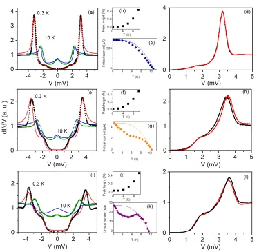
Figure 2.Conductance spectra for junctions withP≤20% (a),P≈97% (e) andP≈99% (i) at 0.3 K and at 10 K. The temperature evolution of the peak at zero bias is shown in (b), (f) and (j) respectively. The peak height is reported on Y axis as the ratio between the zero bias peak height and the height of the peak corresponding to the superconducting gap. Panels (d), (h) and (l) show the overlap of the positive and negative branch of the curves at 0.3 K for the three samples mentioned above. The shift between the two branches is proportional to the ferromagnetic exchange energy. In panels (c), (g) and (k) we show the critical current as a function of temperature (diamonds), in comparison with the standard behavior of Josephson junctions with insulating barriers.
3 Conductance measurements
Measurements of IV curves as a function of temperature highlighted an anomalous IC(T)
behavior for junctions with barrier thicknesses above 3 nm, which has been extensively dis-cussed in [7]. In that work, the relevance of the magnetic activity of the barrier is disdis-cussed, and a phenomenological model to describe the anomalousIC(T) curves is detailed. Here we
present measured dI/dV curves and their relation with the presence of triplet coupling inside
In Fig. 2 (a), (e) and (f) are shown the conductance spectra for three junctions with different spin filter efficiencies (<20%, 97% and 99%) for two different temperatures. For
all the samples we observe the appearance of two symmetric structures atV ≈ ∆at low
temperatures. Similar structures are observed in the presence of a Zeeman splitting that shifts the spin bands of the superconductor [11]. Since the subgap structures become increasingly pronounced as the spin polarization increases, it is reasonable to assume for our samples that these are due to the exchange field induced in the superconducting electrodes by the GdN barrier. Furthermore, analogous experiments in NbN/GdN/TiN (where TiN is a
non-superconducting metal) do not show any sign of subgap structures, while they show evidence of an exchange field induced in the NbN superconducting electrode [12]. This implies that the structures observed in NbN/GdN/NbN Josephson junctions should be related to the exchange
fields induced by GdN in each of the superconducting electrodes.
In addition, we observe a zero-bias peak starting at 4 K up to 10 K [see Fig. 2 (b), (f) and (j)], and a finite conductance at zero voltage at all temperatures, in contrast with the typical behavior of a standard BCS junction. Similar features have been reported in NbN/GdN/TiN
junctions, where the zero-bias peak has been related to the presence of odd-frequency su-perconducting order [13]. However, since the TiN layer is metallic, the Josephson coupling does not occur and consequently no triplet supercurrent can be observed. In these junctions the zero-bias peak corresponds to the situation where the superconducting density of states (DOS) is enhanced at the Fermi level. Similarly, in NbN/GdN/NbN Josephson junctions, the
zero-bias peak should correspond to an unconventional behavior of the DOS of the super-conducting electrodes in the vicinity of the Fermi level. In order to account for the presence of available states at the Fermi level, one can use the following modified expression for the density of states:
ρ(E)= 1
c+1 Re
(E|E−iΓ|
−iΓ)2−∆ +c
(1)
The fitting parameterΓ accounts for the finite lifetime of the Cooper pairs [14] and it has
been used in plenty of experiments to explain the deviation of the measured curves from the standard exponential subgap of BCS superconductors [15]. As the spin-filter efficiency
increases, we find that the subgap region dI/dV curves becomes almost polynomial instead,
a feature that is reproduced in the simulations by increasing the smearingΓ, thus making it
possible to correlate the shape of the dI/dV curve with the increasing magnetic activity of
the samples. In analogy with the results on NbN/GdN/TiN junctions we include the second
fitting termc, sinceΓalone is not sufficient to account for the finite background conductance
observed experimentally [12, 13]. The conductance formula can be then obtained deriving the following expression for the quasiparticle Josephson current [16–18]:
I∝a
+∞
−∞ ρ1(E
+h)ρ2(E−h+V)f(E)−f(E+V)+
b
+∞
−∞
ρ1(E−h)ρ2(E+h+V)f(E)−f(E+V) (2)
whereρ1andρ2are the DOS in the two superconducting electrodes,f(E) is the Fermi func-tion,aandbare coefficient used to model spin filter efficiency andhis the exchange field of
the ferromagnet. The coefficienta is the spin filter efficiency, estimated fromR(T) curves,
whilebis chosen so thata+b=1.
As we stated before, the exchange fieldhis known to cause the Zeeman splitting of the spin bands in the superconductor, and the appearance of characteristic subgap features in dI/dV curves of superconductor/insulator/normal metal junctions. However, in the case of
In Fig. 2 (a), (e) and (f) are shown the conductance spectra for three junctions with different spin filter efficiencies (<20%, 97% and 99%) for two different temperatures. For
all the samples we observe the appearance of two symmetric structures atV ≈ ∆ at low
temperatures. Similar structures are observed in the presence of a Zeeman splitting that shifts the spin bands of the superconductor [11]. Since the subgap structures become increasingly pronounced as the spin polarization increases, it is reasonable to assume for our samples that these are due to the exchange field induced in the superconducting electrodes by the GdN barrier. Furthermore, analogous experiments in NbN/GdN/TiN (where TiN is a
non-superconducting metal) do not show any sign of subgap structures, while they show evidence of an exchange field induced in the NbN superconducting electrode [12]. This implies that the structures observed in NbN/GdN/NbN Josephson junctions should be related to the exchange
fields induced by GdN in each of the superconducting electrodes.
In addition, we observe a zero-bias peak starting at 4 K up to 10 K [see Fig. 2 (b), (f) and (j)], and a finite conductance at zero voltage at all temperatures, in contrast with the typical behavior of a standard BCS junction. Similar features have been reported in NbN/GdN/TiN
junctions, where the zero-bias peak has been related to the presence of odd-frequency su-perconducting order [13]. However, since the TiN layer is metallic, the Josephson coupling does not occur and consequently no triplet supercurrent can be observed. In these junctions the zero-bias peak corresponds to the situation where the superconducting density of states (DOS) is enhanced at the Fermi level. Similarly, in NbN/GdN/NbN Josephson junctions, the
zero-bias peak should correspond to an unconventional behavior of the DOS of the super-conducting electrodes in the vicinity of the Fermi level. In order to account for the presence of available states at the Fermi level, one can use the following modified expression for the density of states:
ρ(E)= 1
c+1 Re
(E|E−iΓ|
−iΓ)2−∆ +c
(1)
The fitting parameterΓ accounts for the finite lifetime of the Cooper pairs [14] and it has
been used in plenty of experiments to explain the deviation of the measured curves from the standard exponential subgap of BCS superconductors [15]. As the spin-filter efficiency
increases, we find that the subgap region dI/dV curves becomes almost polynomial instead,
a feature that is reproduced in the simulations by increasing the smearingΓ, thus making it
possible to correlate the shape of the dI/dV curve with the increasing magnetic activity of
the samples. In analogy with the results on NbN/GdN/TiN junctions we include the second
fitting termc, sinceΓalone is not sufficient to account for the finite background conductance
observed experimentally [12, 13]. The conductance formula can be then obtained deriving the following expression for the quasiparticle Josephson current [16–18]:
I∝a
+∞
−∞ ρ1(E
+h)ρ2(E−h+V)f(E)−f(E+V)+
b
+∞
−∞
ρ1(E−h)ρ2(E+h+V)f(E)−f(E+V) (2)
whereρ1andρ2are the DOS in the two superconducting electrodes, f(E) is the Fermi func-tion,aandbare coefficient used to model spin filter efficiency andhis the exchange field of
the ferromagnet. The coefficientais the spin filter efficiency, estimated fromR(T) curves,
whilebis chosen so thata+b=1.
As we stated before, the exchange fieldhis known to cause the Zeeman splitting of the spin bands in the superconductor, and the appearance of characteristic subgap features in dI/dV curves of superconductor/insulator/normal metal junctions. However, in the case of
very high spin polarization one of the two bands is almost completely suppressed, and thus
the main signature of the Zeeman splitting in dI/dV curves is a voltage shift corresponding
to the actual exchange energy induced in the superconductor, as observed in NbN/GdN/TiN
junctions [12, 13]. In order to estimateh, we analyzed the symmetry of the conductance spectra of samples with different barrier thicknesses. In Fig. 2 (d), (h) and (l), the positive
and negative branch of the differential conductance are superimposed. For the junction with
lowest spin filter efficiency the two branches overlap, indicating the absence of a significant
exchange field. Assuming an exchange energy with the same magnitude but opposite sign in the two electrodes, the difference between the positive and negative peaks of the conductance
is proportional toh.
The magnetic field corresponding to the exchange energyhis given by:
µ0H= 2ehgµ
B (3)
whereµ0is the vacuum permittivity,eis the electron charge,gis the Lande factor, which is 2 for GdN, andµBis the Bohr magneton. For the junctions shown in Fig. 2 (h) and (l) the values
obtained for the exchange field are respectivelyµ0H=0.43±0.2Tandµ0H=−0.17±0.1T. These values are far larger than the typical values of the Fraunhofer modulation in these junctions. The sign of the exchange field is inverted between the two junctions with high spin polarization and the absolute value decreases with increasing barrier thickness. This last result is in agreement with previous observations of a decreasing barrier height with increasing GdN thickness, due to the presence of two Schottky barriers at the interfaces, rather than a conventional square barrier, while the sign inversion of the exchange fieldH can be attributed to the changes in the unsaturated GdN domain structure occurring at larger thicknesses [19].
The fitting curves in Fig. 2 show that Eq. 2 reproduces the experimental data with good approximation, thus supporting the hypothesis of an unconventional DOS at the Fermi level related to the exchange fields induced in the superconducting electrodes. In junctions with high spin polarization, Eq. 2 describing the quasi-particle current gives a very rough repro-duction of the measured dI/dV curve. This result can be compared with the one reported in
[7], where theIC(T) behavior can be only roughly reproduced without considering a much
more complex magnetic structure of the barrier, including a strong asymmetry in the induced exchange fields. These experimental indications of an increasing asymmetry in the exchange fields induced in the NbN electrodes coming from both dI/dV measurements andIC(T) curves
[Fig. 2 (c), (g) and (k)] are compatible with the presence of spin-triplet transport mechanisms contributing to the total supercurrent in spin-filter Josephson junctions.
4 Conclusion
The previous observations of anomalousIC(T) curves for high spin filter efficiencies imply
the presence of spin-triplet supercurrents in NbN/GdN/NbN Josephson junctions. The subgap
structures and the zero bias peak observed in the conductance spectra analyzed in this work are attributed to an asymmetric induced exchange field in the superconducting electrodes and to a finite background conductance caused by a non-conventional density of states in the superconducting electrodes compatible with equal-spin Cooper pairs contributing to the total current.
References
[2] S. Kawabata, Y. Asano, T. Tanaka, A. A. Golubov, and S. Kashiwaya, Phys. Rev. Lett.
104, 117002 (2010).
[3] M. Fogelstrom, Phys. Rev. B62, 11812-11819 (2000).
[4] K. Senapati, M. G. Blamire, Z. H. Barber, Nature Materials10, 849-852 (2012). [5] A. Pal, Z. H. Barber, J. W. A. Robinson and M. G. Blamire, Nature Communications5,
3340 (2014).
[6] D. Massarotti, A. Pal, G. Rotoli, L. Longobardi, M. G. Blamire and F. Tafuri, Nature Communications6, 7376 (2015).
[7] R. Caruso, D. Massarotti, G. Campagnano, A. Pal, H. G. Ahmad, P. Lucignano, M. Eschrig, M. G. Blamire and F. Tafuri, Phys. Rev. Lett.122, 047002 (2019).
[8] L. Longobardi, D. Massarotti, G. Rotoli, D. Stornaiuolo, G. Papari, A. Kawakami, G. P. Pepe, A. Barone and F. Tafuri, Appl. Phys. Lett.99, 062510 (2011).
[9] D. Stornaiuolo, G. Rotoli, D. Massarotti, F. Carillo, L. Longobardi, F. Beltram, and F. Tafuri, Phys. Rev. B87, 134517 (2013).
[10] D. Stornaiuolo, D. Massarotti, R. Di Capua, P. Lucignano, G. P. Pepe, M. Salluzzo, and F. Tafuri, Phys. Rev. B95, 140502 (2017).
[11] R. Meservey, P. Tedrow, and P. Fulde, Phys. Rev. Lett.25, 1270 (1970). [12] A. Pal and M. G. Blamire, Phys. Rev. B92, 180510(R) (2015)
[13] A. Pal, J. A. Ouassou, M.Eschrig, J. Linder and M. G. Blamire, Scientific Reports7, 40604 (2016).
[14] R. C. Dynes, V. Narayanamurti, and J. P. Garno, Phys. Rev. Lett.41, 1509 (1978). [15] E. L. Wolf, Principles of Electron tunneling spectroscopy(Oxford University Press,
Oxford, 2nd edition, 2011)
[16] R. Meservey and P. M. Tedrow, Phys. Rev. B11, 4224-4236 (1975). [17] X. Hao, J. S. Moodera, R. Meservey, Phys. Rev. B428235-8244 (1990).
[18] P. M. Tedrow, J. E. Tkaczyk and A. Kumar, Phys. Rev. Lett.56, 1746-1749 (1986). [19] A. Pal, K. Senapati, Z. H. Barber, and M. G. Blamire, Adv. Mater. 25, 5581-5585