University of Windsor University of Windsor
Scholarship at UWindsor
Scholarship at UWindsor
Electronic Theses and Dissertations Theses, Dissertations, and Major Papers
1999
A multiple in-camera processing system for machine vision.
A multiple in-camera processing system for machine vision.
Roberto. Muscedere
University of Windsor
Follow this and additional works at: https://scholar.uwindsor.ca/etd
Recommended Citation Recommended Citation
Muscedere, Roberto., "A multiple in-camera processing system for machine vision." (1999). Electronic Theses and Dissertations. 675.
https://scholar.uwindsor.ca/etd/675
This online database contains the full-text of PhD dissertations and Masters’ theses of University of Windsor students from 1954 forward. These documents are made available for personal study and research purposes only, in accordance with the Canadian Copyright Act and the Creative Commons license—CC BY-NC-ND (Attribution, Non-Commercial, No Derivative Works). Under this license, works must always be attributed to the copyright holder (original author), cannot be used for any commercial purposes, and may not be altered. Any other use would require the permission of the copyright holder. Students may inquire about withdrawing their dissertation and/or thesis from this database. For additional inquiries, please contact the repository administrator via email
INFORMATION TO USERS
This manuscript has been reproduced from the microfilm master. UMI films the text directly from the original or copy submitted. Thus, some thesis and dissertation copies are in typewriter face, while others may be from any type of computer printer.
The quality of th is reproduction is dependent upon the quality of the copy subm itted. Broken or indistinct print, colored or poor quality illustrations and photographs, print bleedthrough, substandard margins, and improper alignment can adversely affect reproduction.
In the unlikely event that the author did not send UMI a complete manuscript and there are missing pages, these will be noted. Also, if unauthorized copyright material had to be removed, a note will indicate the deletion.
Oversize materials (e.g., maps, drawings, charts) are reproduced by sectioning the original, beginning at the upper left-hand comer and continuing from left to right in equal sections with small overlaps.
Photographs included in the original manuscript have been reproduced xerographically in this copy. Higher quality 6" x 9” black and white photographic prints are available for any photographs or illustrations appearing in this copy for an additional charge. Contact UMI directly to order.
ProQuest Information and Learning
300 North Zeeb Road. Ann Arbor, Ml 48106-1346 USA 800-521-0600
A Multiple In-Camera Processing System for Machine Vision
by
Roberto Muscedere
A Thesis
Submitted to the College o f Graduate Studies and Research through the Department of Computer and Electrical Engineering in partial fulfillment o f the
requirements for the Degree o f Master o f Applied Science at the University of Windsor
Windsor, Ontario, Canada
September 1999
1 * 1
of CanadaNational LibraryAcquisitions and Bibliographic Services
395 Wellington Street Ottawa ON K1A0N4 Canada
Biblioth&que nationale du Canada
Acquisitions et
services bibliographiques
395, rue Wellington Ottawa ON K1A0N4 Canada
Yourm
Our lit Nan rMitnct
The author has granted a non
exclusive licence allowing the
National Library of Canada to
reproduce, loan, distribute or sell
copies of this thesis in microform,
paper or electronic formats.
The author retains ownership of the
copyright in this thesis. Neither the
thesis nor substantial extracts from it
may be printed or otherwise
reproduced without the author’s
permission.
L’auteur a accorde une licence non
exclusive permettant a la
Bibliotheque nationale du Canada de
reproduire, preter, distribuer ou
vendre des copies de cette these sous
la forme de microfiche/film, de
reproduction sur papier ou sur format
electronique.
L’auteur conserve la propriete du
droit d’auteur qui protege cette these.
Ni la these ni des extraits substantiels
de celle-ci ne doivent etre imprimes
ou autrement reproduits sans son
autorisation.
0-612-62258-4
© 1999 Roberto Muscedere
All Rights Reserved. No part o f this document may be reproduced,
stored or otherwise retained in a retrieval system or transmitted in
any form, on any medium or by any means without the prior written
permission o f the author.
Approved By:
Dr. A. Jaekel (External examiner)
Dr. M. Ahmadi (Internal Reader)
J- SoJ|i^(Internal Reader)
Dr. G.A. Jullien (Supervisor)
7 )/ l ~
Abstract
In a typical machine vision application, a line-scan camera positioned on the production
line captures images o f the parts to be inspected and sends them to the machine vision
computer. The computer then uses high-speed data acquisition devices and sophisticated
analysis software to extract information from these cameras and generates decisions about
the product and manufacturing system. As the manufacturing systems increasingly gener
ate more fine featured and advanced products, the need for higher resolution and faster
processing of these camera images is necessary to maintain quality control.
To reduce the overwhelming amount of data from multiple camera systems to the analysis
computer, an in-camera processing system is introduced. This system involves placing a
computing system inside the camera which can perform similar operations to the analysis
system, but without all of the additional overhead components.
The work presented in this thesis describes an enhanced embedded system which is
mounted into a DALSA line-scan camera. This system provides support for real-time one
dimensional signal processing with the aid o f integrated hardware and software resources.
iv
Acknowledgments
There are several people who deserve my sincere thanks for their generous contributions to this project.
1 would first like to thank my supervisor Dr. G. A. Jullien for his guidance, advice and for bringing this challenging project to my attention. I am grateful to Dalsa Inc. for providing funding, the camera systems, privileged technical information and their services in assem bling the PCBs. I would also like to thank Hossain Hajimowlana for creating algorithms which demonstrated this projects capabilities, and my committee members Dr. Arunita Jaekel, Dr. Majid Ahmadi and Dr. James Soltis.
I would also like to recognize the following individuals and corporations for their contri butions: Marjan Shahkarami for her time and comments on the first drafts o f this thesis, CMC for providing and supporting the design software and computing hardware which made this project possible, Micronet R&D for providing financial and networking support, Robert Mavrinac for donating additional computing and networking resources, Joe Novosad for his input on practical PCB designing, and Bruce Watt for his help in imple menting post-design changes.
Table of Contents
C h ap ter 1 Introduction...l
1.1 Introduction... 1
1.2 In-Camera Processing B oard... 4
1.3 First Generation System... 5
1.4 Thesis O verview ...5
1.5 Thesis Organization... 6
C h ap ter 2 F irst G eneration 2.1 Introduction...7
2.2 Camera Specifications... 7
2.3 Theory of Operation... 8
2.4 First Generation System D etails... 9
Xilinx 4000E Series FPGA ...10
Motorola M 68HC11E9 Microcontroller Unit ... 12
2.5 Detailed System Operation... 15
2.6 Host Communication Interface... 18
2.7 Video Data Processing... 20
Minimum/Maximum Algorithm ...21
Range Algorithm ... 22
Delta Threshold Algorithm ... 23
Delta T r a c k e r ...24
2.8 Data Compression...25
Run-Length Encoding (RLE) Compression ... 26
Real Time RLE Implementation ...27
Modified RLE Compression ... 27
2.9 FPGA Internal FIFO ... 29
2.10 FPGA External FIFO ...30
2.11 Hardware Design Tools... 3 1 Synopsys Design Compiler ... 31
vi
University o f Windsor
XilinxXACT ...32
Microcontroller Assembler ... 32
2.12 Host Software D esign... 32
2.13 Summary...33
Chapter 3
Second Generation System Design ...35
3.1 Introduction...35
3.2 Design Target... 35
3.3 Design Improvements... 36
Field Programmable Gate Array ...36
SRAM Simulated FIFO ...37
RS-232 ...38
3.4 Design Additions... 39
Digital Signal Processor ... 39
Camera To Host Communication ... 44
Programmable Logic ... 55
Bus Exchanger ...57
3.5 Envisioned System...59
Component level ... 59
System Level ...60
3.6 Summary... 61
Chapter 4
Second Generation System Implementation ...62
4.1 Introduction... 62
4.2 Design Implementation...62
Physical Constraints ... 62
Partitioning ... 63
Manual Routing ... 65
Verification ... 66
4.3 PCB Tests... 66
Post Fabrication Testing ... 66
Pre Power Up Testing ...66
4.4 Software T ools...67
DSP Assembler/C Compiler ... 67
Microsoft Visual Studio v6 and Adaptec 1394 API ... 67
4.5 Individual System Test... 67
Stand-Alone Tests ... 68
Camera Tests ...68
4.6 Software Design...70
Second Generation System ... 70
PC Monitoring/Processing System ... 71
4.7 Summary... 72
University o f Windsor
Chapter 5
Operational Tests and Results...74
5.1 Introduction... 74
5.2 Test Setup... 74
5.3 Operational Overview...77
5.4 Realizing a video processing algorithm... 77
Other FPGA Sub-Systems ...78
Algorithm Coding Steps ...78
5.5 FPGA Performance... 79
Video Processing Algorithms ... 80
FIFO Performance ...84
FPGA-to-DSP communication ... 85
5.6 DSP Performance...85
5.7 1394 Performance... 85
5.8 CPLD D evices... 86
5.9 Summary...86
Chapter 6
6.1 Summary and Contributions... 876.2 Suggestions for Future W ork... 88
REFERENCES_______________________________________________________ 90
Appendix A
First Generation System Hardware ...93
A .l Schematics ...94
Page I ... 94
Page 2 ... 95
Page 3 ... 96
A.2 PCB L ay ou t...97
Component Side ...97
Solder Side ...97
A.3 Fabricated B o a rd ... 98
Component Side ...98
Solder Side ...98
A.4 Assembled B o a rd ... 99
Component Side ...99
Solder Side ...99
A.5 Test S etu p ... 100
Appendix B
First Generation System Software Code... 101
viii
University o f Windsor
B .l MCU C o d e ... 101
Code Building Utilities ... 101
Include Files ... 102
Internal EEPROM Code ... 103
Downloadable Modules ...I l l External EEPROM Modules ... 114
B.2 FPGA Hardware Description Code ... 144
Synopsys Design Compiler Procedure and Scripts ...144
Xilinx Scripts ... 147
Main VHDL Code ...148
Video Processor VHDL Code ... 162
B.3 PC Host Software C o d e ... 184
Makefile ...184
Resources ...198
MFC Files ... 209
CLarchApp:CWinApp Class ... 210
CMainFrame Class ... 214
CChildFrame Class ... 220
CLarchCptView Class ...222
CLarchCptDoc Class ... 231
Camlnt Class ...238
Serial Class ...258
UnComp Class ... 272
Comp Class ...280
Comp LComp Class ...285
CGetParams Class ... 290
Video Processor Headers ... 296
Appendix C
Second Generation System Hardware... 299
C. 1 S chem atics...300
FPGA ... 300
DSP ...304
1394 ...310
C.2 PCB L ay o u ts...315
FPGA Board ... 315
DSP Board ...316
1394 Board ...317
C.3 Fabricated B o a rd s ... 318
FPGA Board ... 318
DSP Board ...319
1394 Board ...320
C.4 Assembled Boards ... 321
FPGA Board ... 321
DSP Board ...322
1394 Board ...323
University of Windsor
Appendix D Second G eneration System Softw are Code... 324
D .i DSP C o d e ...324
Firmware Loader ... 324
Firmware Builder ... 329
Firmware Code ... 334
EEPROM Emulator Utilities ...384
D.2 FPGA Hardware D escription...386
Synopsys Scripts ... 386
Xilinx Scripts ... 389
Main VHDL Code ... 390
Video Processor VHDL Code ... 407
Test VHDL Code ...429
D.3 CPLD1 Hardware D escription...437
Synopsys Scripts ...437
VHDL Code ... 438
D.4 CPLD2 Hardware D escription...449
Synopsys Scripts ...449
VHDL Code ... 450
D.5 Main PC Host Software C o d e ... 457
Workspace file ... 457
Project file ... 458
Resources ... 463
MFC Files ... 474
CLarchApp.CWinApp Class ...475
CMainFrame Class ...481
CChildFrame Class ... 486
CLarchCptView Class ... 488
CLarchCptDoc Class ... 498
Camlnt Class ... 507
Physical Class ... 514
Image Class ... 542
Imageline Class ... 550
CCamParams Class ...551
CParams Class ... 555
External Processor Interface ...562
D.6 Focus Processor C o d e ... 566
Project file ... 566
MFC Files ... 568
Resource Files ... 569
Focus Code Files ...570
D.7 Lineup Processor C o d e ... 574
Project file ... 574
MFC Files ... 576
Resource Files ... 577
Lineup Code Files ...578
D.8 Minimum/Maximum Processor C o d e ... 582
x
University o f Windsor
Project file ... 582
MFC Files ... 584
Resource Files ...585
Minmax Code Files ... 586
D.9 Deltatracker Processor C o d e ...591
Project file ... 591
MFC Files ... 593
Resource Files ...594
Deltatracker Code Files ...595
D.IO Fuzzy Logic Processor Code ...600
Project file ... 600
MFC Files ... 602
Resource Files ...603
Fuzzy Code Files ... 604
List of Figures
Figure 1.1 Typical Machine Vision Application...2
Figure 1.2 Capturing an Image from a Non-Synchronized Production L in e... 2
Figure 1.3 Capturing an Image from a Synchronized Production L in e... 3
Figure 1.4 Example o f Image Pixelization Effect... 3
Figure 1.5 Multiple Camera System...4
Figure 1.6 In-Camera Processing Board Reduces Bandwidth to Analysis System 5 Figure 2 .1 C L-E1-1024 System Level Diagram... 8
Figure 2.2 Unmodified High Level System Block Diagram...8
Figure 2.3 First Generation System High Level System Block D iagram ...9
Figure 2.4 First Generation System Component Level D iagram ...10
Figure 2.5 Xilinx 4000E Series C L B ...11
Figure 2.6 Xilinx 4000E Series IO B ...12
Figure 2.7 MCU Sample Memory Interface in Expanded M ode...14
Figure 2.8 Detailed Flowchart o f Main R outine...16
Figure 2.9 Detailed Flowchart o f Capture Routine... 18
Figure 2.10 Block Diagram of Microcontroller to FPGA Comm unication... 19
Figure 2 .11 MCU to FPGA Comm unication... 19
Figure 2.12 FPGA to MCU Comm unication...20
Figure 2.13 CL-E1-1024 Output Signals... 20
Figure 2.14 Video Processing Algorithm Connectivity...21
Figure 2.15 Graphical Interpretation o f the Minimum/Maximum Algorithm...21
Figure 2.16 Detailed Flowchart o f the Minimum/Maximum A lgorithm ... 22
Figure 2.17 Graphical Interpretation o f the Range Algorithm...22
Figure 2.18 Detailed Flowchart o f the Range Algorithm... 23
Figure 2.19 Graphical Interpretation o f the Delta Threshold A lgorithm ... 23
Figure 2.20 Detailed Flowchart o f the Delta Threshold A lgorithm ... 24
Figure 2.21 Graphical Interpretation o f the Delta Tracker A lgorithm ...24
Figure 2.22 Detailed Flowchart o f the Delta Tracker A lgorithm ... 25
xii
University o f Windsor
Figure 2.23 Decomposition of the Compressed Stream...26
Figure 2.24 Compressed Single BLACK Line... 28
Figure 2.25 Compressed Single BLACK Line Using Enhanced Size Encoding...28
Figure 2.26 Example o f Possible Transmission Corruption... 28
Figure 2.27 Example o f Synchronization in a Corrupted Transmission... 29
Figure 2.28 Internal FIFO Structure... 30
Figure 2.29 External FIFO Read/Write/Idle/Reset Operations Flow Diagram... 31
Figure 2.30 Software Development Environment and Host Monitoring Software 33 Figure 3.1 FPGA Serial Slave Interface... 36
Figure 3.2 Block Diagram o f Programmable Synchronous FIFO...38
Figure 3.3 TMS320C52B Memory M ap... 40
Figure 3.4 Block Diagram of DSP and Added External Memory... 41
Figure 3.5 Single Asynchronous Memory Device Connection...42
Figure 3.6 Synchronous Device to DSP Connection...43
Figure 3.7 Implementation of Static I/O with DSP and Extra Logic... 43
Figure 3.8 Synchronous to Asynchronous Transmission Converter... 44
Figure 3.9 Correct and Incorrect 1394 Cable Topologies... 47
Figure 3.10 1394 Cable and Connector... 47
Figure 3.11 Annex J Method o f Galvanic Isolation... 53
Figure 3.12 TI Method o f Galvanic Isolation... 54
Figure 3.13 3.3V PHY Interface to 5V LLC... 55
Figure 3.14 Xilinx 9500 Series CPLD Internal Structure...56
Figure 3.15 Bus Exchanger Internal Structure... 58
Figure 3.16 Envisioned Component Level Block Diagram...60
Figure 3.17 Envisioned System Level Block D iagram ... 61
Figure 4.1 Actual Board Space and All Component Foot Prints...63
Figure 4.2 Power Bus Connectivity... 64
Figure 4.3 Second Generation System Combined with DALSA Camera... 69
Figure 4.4 Firmware EEPROM Layout...70
Figure 4.5 Second Generation System 1394 Memory M ap... 71
Figure 4.6 Command Register B its... 7 1 Figure 4.7 PC Monitoring/Processing System C++ Classes... 72
Figure 5.1 Testing Environment... 75
Figure 5.2 Test F ixture... 76
Figure 5.3 FPGA Sub-Systems... 78
Figure 5.4 Examples o f Patterned Backgrounds...81
Figure 5.5 Block Diagram o f a Fuzzy Logic System... 81
Figure 5.6 Fuzzy Component Level Diagram in FPGA... 82
Figure 5.7 Block Diagram o f the AR Predictor... 83
Figure 5.8 Monitoring/Processing System Operating in Real T im e...84
Figure 5.9 AR Predictor Examples... 84
List of Tables
Table 2.1 MCU Baud Rates Related to Crystal Oscillator and Divider... 13
Table 2.2 Top Level System Com m ands...15
Table 2.3 Capture Level Commands... 17
Table 2.4 Examples of RLE Compressed Byte Streams... 26
Table 3.1 TSB12C01A Memory Map...50
xiv
List of Abbreviations
ALU Arithmetic Logic Unit
API Application Program Interface
AR Auto Regressive
ATF Asynchronous Transmit FIFO
ATM Asynchronous Transfer Mode
bps Bits Per Second
Bps Bytes Per Second
BUFFALO Bit U ser’s Fast Friendly A id to Logical Operation
CCD Charge Coupled Device
CLB Configurable Logic Block
CMOS Complimentary M etal Oxide Semiconductor
CPLD Complex Programmable Logic Device
CRC Cyclic Redundancy Check
CSR Control and Status Registers
DARAM Dual Access Random Access Memory
DFF Data Flip Flop
DLL Dynamic Link Library
DPRAM Dual Port Random Access Memory
DSP D igital Signal Processor
EEPROM Electrically Erasable Programmable Read Only Memory
EPROM Electrically Programmable Read Only Memory
FB Function Blocks
FIFO First In First Out
University o f Windsor
GRF General Receive FIFO
GUI Graphical User Interface
I/O Input/Output
IBM International Business Machines
IEEE Institute o f Electrical and Electronics Engineers
IOB Input/Output Block
ITF Isochronous Transmit FIFO
JTAG Joint Test Action Group
LLC Link Layer Controller
MAC Multiply and Accumulate
M CU Microcontroller Unit
PC Personal Computer
PCB Printed Circuit Board
PCI Peripheral Component Interconnect
PHY Physical Interface
PLCC Plastic Lead Chip Carrier
PEL Phase Locked Loop
RAM Random Access Memory
RLE Run Length Encoding
ROM Read Only Memory
SCSI Small Computer Simple Interface
SRAM Static Random A ccess Memory
TI Texas Instruments
TDI Time Delay Integration
VHDL VHSIC Hardware Description Language
VHSIC Very High Speed Integrated Circuit
V U W Very Long Instruction Word
xvi
Chapter 1
Introduction
Introduction
1.1
Introduction
Human vision has played an indispensable role in the process of
manufacturing products since the beginning of the Industrial
Revolution. Human eyes did what no machines could do
themselves by locating and positioning work, tracking the flow of
parts, and inspecting output for quality and consistency. The
requirements today of many manufacturing processes have
surpassed the limits o f human eyesight. Manufactured items often
are produced too quickly or with tolerances too small to be
analyzed by the human eye. In response to manufacturers' needs, a
new technology known as “machine vision” emerged, providing
manufacturing equipment with the gift o f sight.
In a typical machine vision application, a special video camera
positioned on the production line captures images of the parts to be
inspected and sends them to the machine vision computer. The
computer then uses sophisticated analysis software to extract
information from these digital images and generates decisions
about the product manufacturing system (see Figure 1.1).
University o f Windsor
Figure 1.1 Typical Machine Vision Application
Products Under Inspection
Manufacturing Line
Special Video Cam era
Image Analysis System
Process Control/ Controller Alert
System
For a moving production line, a standard frame camera (operating at NTSC 60Hz, - 15kHz
line rate) is not capable o f capturing true images since there is no synchronization between
the camera and the manufacturing line (see Figure 1.2). Even if their speeds are matched,
there still will be some losses causing image distortion due to the nature of the frame
camera.
Figure 1.2 Capturing an Image from a Non-Synchronized Production Line
Manufacturing Line | Camera Frame Capturing (60Hz) Image Analysis System
A special continuously capturing camera (line scan) that is synchronized to the motion o f
the manufacturing line will compensate for the image quality loss o f a standard frame
camera (see Figure 1.3).
Introduction Introduction
University o f Windsor
Figure 1.3 Capturing an Image from a Synchronized Production Line
Line Scan Camera (synchronized with manufacturing line)
Manufacturing Line Image Analysis System
To obtain an accurate digital representation o f the image, the camera must be placed an
appropriate distance away from the manufacturing line. If the camera is placed too far
away from the manufacturing line, important data may be lost by the image pixelization
effect (see Figure 1.4).
Figure 1.4 Example of Image Pixelization Effect
&
Pixelization
To eliminate the problem of image pixelization, multiple cameras can be placed side-by-
side and their separate images can be combined by the analysis system into a single
complete image (see Figure 1.5).
University o f Windsor
Figure 1.5 Multiple Camera System
90
c/5
Line Scan C am era
Line Scan Cam era
High Bandwidth Data
t
Line Scan C am era
I I
M anufacturing Line
Image Analysis System
Product Under Inspection
I * '
Although multiple cameras solve the pixelization problem, they create a new high
bandwidth problem. Similarly as manufacturing system speeds have surpassed the speed
o f human vision, the computational time for processing very large amounts o f image data
can overwhelm the image analysis system. To resolve this high bandwidth problem, an in
camera processing board concept is introduced [16].
1.2
In-Camera Processing Board
The concept of the in-camera processing board is simple: Place a computing system inside
the camera which can perform similar operations to the analysis system, but without all of
the additional overhead components (large operating system, graphical user interface, hard
disk, video support, etc.). This in-camera system will then reduce the outgoing bandwidth
to the analysis system so that it can handle data from multiple cameras (see Figure 1.6).
Introduction In-Camera Processing Board 4
University o f Windsor
Figure 1.6 In-Camera Processing Board Reduces Bandwidth to Analysis System
I
Low Bandwidth Data
1 —
In-Camera Processing Board
In-Camera Processing Board
Line Scan Camera
Line Scan C am era
In-Camera Processing Board
Line Scan C am era
n
Image Analysis System
M anufacturing Line
Product Under Inspection
i * " "
Due to PCB space limitations inside the cameras, the early in-camera system used a single
Field Programmable Gate Array (FPGA) to perform real-time processing directly on the
camera’s digital video stream. Such a system is limited in its processing capabilities and is
unable to perform the higher level image processing required for two dimensional image
data analysis.
1.3
First Generation System
A previous research project used a design based on the above system to transmit the
processed data from the FPGA over a lower bandwidth bi-directional medium. The
permanently programmed FPGA is replaced with an in-system reprogrammable FPGA to
allow the processing algorithms to be easily changed. This new system also included a
FIFO (simulated by a RAM device) and a microcontroller unit (MCU) to facilitate system
control and the bi-directional communication [IS].
1.4
Thesis Overview
The work performed for this dissertation was the design o f a second generation in-camera
processing system which improved upon the first generation system described above. This
new system also includes a Digital Signal Processor (DSP) for enhanced arithmetic and
University o f Windsor
high-speed networking to greatly improve communication to the analysis system and other
cameras.
1.5
Thesis Organization
This thesis is organized as follows: Chapter 2 provides information o f the first generation
system designed prior to this project work. It forms the basis for the decisions made in the
second generation system. Chapter 3 introduces the reasoning behind the selection o f the
devices and components for the second generation system. It also covers the basic
connectivity issues in enabling the systems operation. Chapter 4 lists the design
partitioning steps to realize the system design while maintaining the constraints of the
camera. Hardware tests to verify the design’s proper fabrication are also explained.
Chapter 5 examines the hardware, software and video algorithms performances and offers
potential system design improvements. Chapter 6 concludes this thesis by making
recommendations on a future third generation system.
Introduction Thesis Organization
Reproduced with permission of the copyright owner. Further reproduction prohibited without permission.
Chapter 2
First Generation
System
2.1
Introduction
The first generation system was designed prior to the beginning of
this work by other students. The state of this system was at the point
of initial hardware testing and software design. Before any work
could be done on designing the second generation system, the first
generation system needed to be evaluated and tested to determine
which components of the system would operate within
specifications and which systems needed to be modified, improved
or removed.
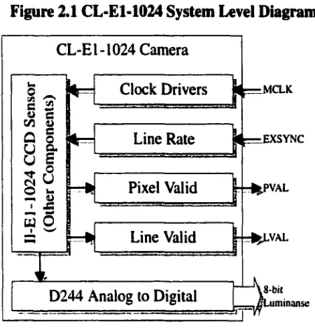
2.2 Camera Specifications
The first generation system was designed for the DALSA CL-E1-
1024 line scan camera. This camera operates at a clock speed of
ISMHz with an 8 bit luminance image data rate o f 7.5MHz and a
maximum line rate of approximately 7.5kHz [5]. The clock source
of the camera is provided by an external generator and the line rate
is controlled by a conveyor or other data rate synchronizing device
(see Figure 2.1). The first generation system was physically
designed to mount directly into the camera and to connect to the
camera’s internal signals and buses.
University o f Windsor
Figure 2.1 CL-E1-1024 System Level Diagram
CL-El-1024 Camera
MCLK
2 12
-Lme
Rate
SYNCU a
Pixel Valid 'VAL — U
£
U O
8-bit [Luminanse
Line Valid Clock Drivers
D244 Analog to Digital
2.3
Theory of Operation
The CL-El-1024 camera alone has a basic interface. Upon reset, the camera begins
transmitting high bandwidth data immediately based on the state of the line valid and
clock signals, it is then the responsibility of a digital data acquisition system to process or
capture the video data. This is strictly a unidirectional communication relationship; no
data from the host ever goes back to the camera (see Figure 2.2).
Figure 2.2 Unmodified High Level System Block Diagram
Uni-Directional High Bandwidth Communication
Camera Clock
Generator Conveyor
Host Monitoring System (DA board)
First Generation System Theory o f Operation 8
University o f Windsor
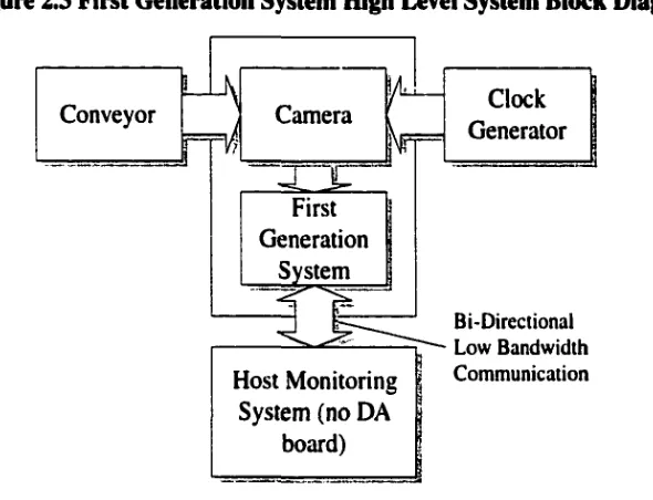
With the addition of the first generation system, the behaviour of the camera interface
changes into a more complex device. The target operation o f the system is to reduce the
incoming uncompressed data stream from the camera and to transmit it to the host
computer over a bidirectional lower bandwidth medium. Although the concept seems
simple, it is much more difficult to implement within the systems constraints (see Figure
2.3).
Figure 2.3 First Generation System High Level System Block Diagram
Clock Generator
Bi-Directional Low Bandwidth Com munication
2.4
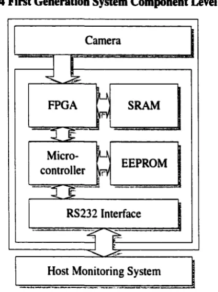
First Generation System Details
The first generation system consists o f a FPGA (to perform real time processing on the
digital video stream from the camera), a SRAM (intended for use as a FIFO to compensate
for large data bursts of the processed data), a microcontroller (the main controlling unit of
the system), an EEPROM (to store microcontroller code and FPGA bitstreams) and a
voltage level converter for RS-232 communication to the host monitoring system (see
Figure 2.4).
Conveyor
rrV^
Camera
First Generation
System
\h
Host Monitoring System (no DA
board)
University o f Windsor
Figure 2.4 First Generation System Component Level Diagram
Camera
FPGA SRAM
Micro
controller EEPROM
33
RS232 Interface
Host Monitoring System
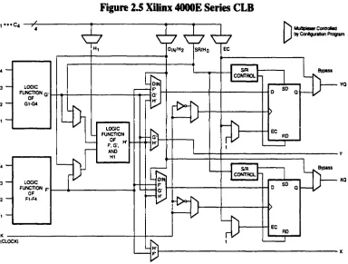
2.4.1 Xilinx4000E Series FPGA
The Xilinx Field Programmable Gate Arrays (FPGAs) are high-performance, high-
capacity SRAM based devices which require programming after reset or power up. Other
FPGA manufacturers (such as Altera) produce PROM based FPGAs which can be
programmed only once. The Xilinx FPGAs have a long programming life cycle and are
ideal for this particular application where the FPGA is intended to be programming for
different algorithms. The 4000 series devices are implemented with a regular,
programmable architecture of Configurable Logic Blocks (CLBs), interconnected by a
hierarchy o f routing resources, and surrounded by a perimeter of programmable Input/
Output Blocks (IOBs). Each 4000E series CLB (see Figure 2.S) contains two 4-bit
function generators (16x1 lookup tables) with fast carry logic, two clocked (edge or level
triggered) “D” flip flops and several multiplexer options which can allow for routing very
dense designs. The 4000E series offers the ability of using the two function generators as
true RAM elements. Each function generator can be used as a 4-bit dual port RAM or both
can be merged into a 5-bit single port RAM. This feature allows each CLBs to contain up
First Generation System Fust Generation System Details 10
University of Windsor
to 34 bits o f RAM (only 2 bits per CLB in the 4000 series) thus enabling the ability to
realize more complex designs in the FPGA.
Figure 2.5 Xilinx 4000E Series CLB
MuJtDiestf CcntrcMd by Configuration Program
EC
B yptss
OIN YQ
OIN XQ
(CLOCK)
srn
CONTROL
sm
CONTROL
LOGIC FUNCTION
OF u
F . a . H AND
Ht
EC SO
RD
RO LOGIC
FUNCTION P OF F1-F4 LOGIC FUNCTION
OF
G1-G4
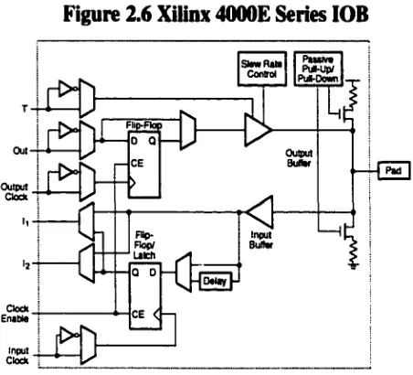
Each 4000E IOB contains two edge triggered “D” flip-flops with enable lines (one for
input and one for output), tri-state control and pull-up and pull-down resistors (see Figure
2.6). This is significantly different from the 4000 predecessor which had no resistors or
flip-flop enable functions which had to be implemented in the CLBs.
University o f Windsor
Figure 2.6 Xilinx 4000E Series IOB
Out Output
Buffer
Pad Output
Clock
Input Buffer
input Clock
Originally, the first generation system used a Xilinx 4003A-6 FPGA. It was decided to
upgrade to a faster 4000E series device since the original was found to be too slow (6ns
CLB delay) to handle the 15MHz clock rate and it did not have the appropriate elements to
allow for efficient implementation o f RAM elements.
2.4.2 Motorola M68HC11E9 Microcontroller Unit
The M68HC11 E series of 8-bit microcontroller units (MCU) combine the M68HCU
CPU with on-chip peripherals. The E series is comprised o f many devices with various
configurations o f RAM, ROM or EPROM, and EEPROM. The particular device used here
in this design is the E9 series in a 68 pin PLCC package which contains 12K o f ROM
(internal BUFFALO monitor for interactive debugging) 512 bytes of EEPROM
(programmed code may be executed by internal bootstrap) and 512 bytes o f RAM. When
in single-chip mode, this device has 40 I/O pins (of differing capabilities) available to the
designer.
The MCU is the heart o f the first generation system as it is responsible for the operation of
the whole embedded system. Its tasks include programming the FPGA, transferring data
to and from the EEPROM, and to relay data from the host to the FPGA and vice versa.
First Generation System First Generation System Details 12
University o f Windsor
System To Host Transmission
The MCU is connected to the host system by means of an RS-232 link. This link is chosen
due to its large noise margin (-12V to 12V) which is not easily effected by electrically
noisy environments and long transmission distances. The MCU itself outputs and expects
TTL signals. An RS-232 voltage level converter is added to the system to transparently
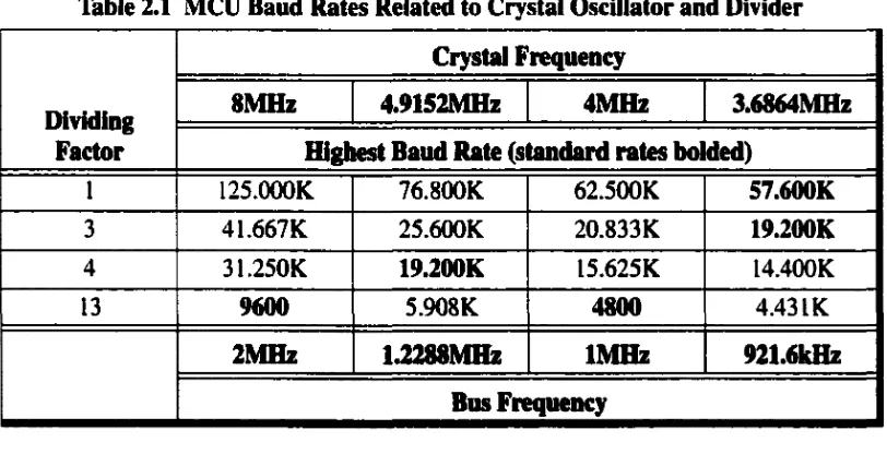
adjust for these necessary voltage changes. The speed o f this link is chosen to be 9600
baud which is determined by a baud rate generator that divides the MCU’s 8MHz crystal
oscillator by 13 (see Table 2.1). Since the baud rate is dependent on the driving oscillator,
various transmission speeds can be obtained. Most of these speed combinations are not
standard and will therefore make it difficult to interface to other standard RS-232 systems
such as the ones provided on IBM compatible PCs. Although it is possible to increase the
speed of the RS-232 link by lowering the MCU clock speed, this was not done since it
would result in a significant overall MCU performance deterioration.
Table 2.1 MCU Baud Rates Related to Crystal Oscillator and Divider
Dividing
Factor
Crystal Frequency
8MHz
4.9152MHz
4MHz
3.6864MHz
Highest Baud Rate (standard rates bolded)
1 125.000K 76.800K 62.500K
57.600K
3 41.667K 25.600K 20.833K
19.200K
4 31.250K
19.200K
15.625K 14.400K13
9600
5.908K4800
4.43 IK2MHz
1.2288MHz
1MHz
921.6kHz
Bus Frequency
EEPROM Connectivity
As mentioned above, the MCU is also connected to an external EEPROM device [34].
This device is required to store the FPGA configuration bitstream and any additional
MCU code since the RS-232 transmission speeds restrict download speeds from the host
to the camera to an unacceptable value. The MCU has the ability to connect to external
University o f Windsor
memory devices through it’s “expanded mode” [14], however, this is not the approach
taken here. The expanded mode feature will perform external memory read/writes for
memory locations which are not mapped to the internal MCU memory model. This mode
also requires several multiplexed I/O pins (address, data, handshaking) in order to address
the maximum 64K external memory range. The capacity o f the EEPROM in this system is
32K bytes (was originally 16K bytes), and therefore the design does not require the full
addressing range and additional external control logic (as seen in Figure 2.7). Instead, an
indirect addressing method o f connectivity is chosen (see schematic in Appendix A.l
"Schematics" on page 94). By using the user I/O pins available from the MCU (when in
single-chip mode), all data, address and control lines are connected; however, the
EEPROM access is controlled by setting these I/O signals with specific microcontroller
software code.
Figure 2.7 MCU Sample Memory Interface in Expanded Mode
P87 PS6 PB5 PB4 PBS PB2 PB1 PSO PC7 PCS PCS PC4 PCS PCS PCI PCO AS R/W
MCU
■ ADDR15 -AD0R14 ■ ADDR13 -ADDR12 •ADDR11 • ADDR10 -ADDR9 -A 00R 8 HC373 01 at 02 02 OS 03 04 04 OS as 08 as 07 07 08 08 LE OE= t >
■ ADDR7 ■A0DR6 -ADDR5 ■AD0R4 -ADDR3 - A0DR2 • A0DR1 - AODRO SHE
•CE
• DATA7 -0ATA6 -0ATA5 •DATA4 •0ATA3 •DATA2 • 0ATA1 -0ATA0First Generation System Fust Generation System Details 14
University o f Windsor
FPGA Connectivity
The MCU connects to the FPGA using a parallel structure. The configuration of the FPGA
is set to require a parallel download (determined by 3 pins on the FPGA tied to power/
ground in a particular combination) with hardware handshaking. Along with the
handshaking lines are special programming and error signals. With all of these
connections and proper software code, the MCU will program the FPGA reliably without
any flaws.
2.5
Detailed System Operation
Upon system reset, the MCU boots up by executing the main code within its internal
EEPROM memory. This internal EEPROM code also contains a series of routines
common to all of the system microcontroller functions. These routines include code that
interfaces to the RS-232 communication port and handles the external EEPROM as a
virtual disk where all MCU code and FPGA bitstreams can be loaded and saved. As
mention previously, the EEPROM is necessary due to the slow speed o f the RS-232 link. If
the FPGA were to be programmed with data directly from the host computer, the time
required would be IS seconds; a considerable and unacceptable delay.
This main routine initializes all the on-board devices and synchronizes with and waits for
commands from the host monitoring system (see Figure 2.8). These commands are
completely programmable by the host and range in function from programming the FPGA
to upgrading the firmware (see Table 2.2).
Table 2.2 Top Level System Commands
Command
Explanation
0x20 Executes the following 236 bytes o f code at memory location 0x0100
0x21 Download microcontroller code into EEPROM
0x22 Download bit stream from host to EEPROM
0x23 Reset FPGA, download contents o f EEPROM bit stream to FPGA and begin capture routine
0x24 Delete microcontroller code from EEPROM
University o f Windsor
Table 2.2 Top Level System Commands
Command
Explanation
0x25 Download FPGA algorithm properties to EEPROM
0x26 Upload FPGA algorithm properties from EEPROM
0x03 Exits to BUFFALO Monitor for interactive system debugging
Figure 2.8 Detailed Flowchart of Main Routine
Reset Variables
Load and Execute
j
Program C-0x20 I 0x20<C<0x30Input 256 bytes to
0x100 C=0x20
Execute Code At 0x0100
C=0x03
Yes
. . . %____
Execute BUFFALO
M onitor
First Generation System Detailed System Operation 16
University o f Windsor
When a valid bitstream is present in the external EEPROM, the processing or capture
phase can begin (see Figure 2.9). This portion o f the system behaves like the main routine
where different commands are executed from the host (see Table 2.3).
Table 2 3 Capture Level Commands
Command
Explanation
0x41 Enable FPGA data processing
0x42 Disable FPGA data processing
0x43 Reset FPGA internal and external FIFOs
0x44 Transmit a parameter to the FPGA
0x45 Begin upload o f FIFO’s popped contents
0x01 Return to top level
University o f Windsor
Figure 2.9 Detailed Flowchart of Capture Routine
Program FPGA with current bitstream in EEPROM
Set program m ing lines I/O to serial
configuration
r [ Capture=FALSE f t Y e s ^ C = 0 x 4 2 ^ % N o C=0x41 Capture=TRUE
jr
YCS/ ( H & L ) - Pulse FIFO RESET * Y e sSend 11 LSB bits of H & L to FPGA
Non-Blocking
C=0x45
Pop a byte (B) from the FPGA external FIFO
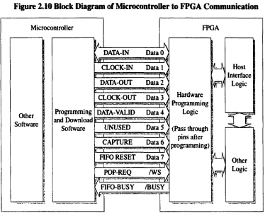
2.6
Host Communication Interface
After the microcontroller programs the FPGA by the parallel programming method, the
programming lines are then treated as serial communication signals to the FPGA logic.
The microcontroller can either send data (programmable algorithm parameters), receive
data (popped contents from external FIFO) or read/write data using static logic control
lines (see Figure 2.10).
First Generation System Host Communication Interface IS
University o f Windsor
Figure 2.10 Block Diagram of Microcontroller to FPGA Communication
M icrocontroller
Programming and Download
Software
= 8
DATA-IN
EZX
UNUSED
r—r
Kf
FPGA
DataO
3
:CLOCK-IN D ata I
i
DATA-OUT D ata 2
CLOCK-OUT Data 3
DATA-VALID D ata 4
Data 5
CAPTURE Data 6
i
FIFO RESET Data 7
POP-REQ /W S
FIFO-BUSY /BUSY
Hardware Programming
Logic
(Pass through pins after programming)
Interface
In order to send data from the MCU to the FPGA a simple clocked unidirectional
hardware serial communication method is used (shown in Figure 2.11) which requires 3
output signal lines.
Figure 2.11 MCU to FPGA Communication
FPGA
-D a ia - O u trij -Clock-O utrfc
— rData-Validrl^
£ £ £ £ £ £
Q Q Q Q a a a a
3x8 Decoder
— Enable 0 - |j — Enable !•
Register 0
Register I
J p r Enable 7 r || R egister7_______
Video Processing Algorithm
University o f Windsor
Receiving data from the FPGA uses a bi-directional hardware serial communication
method (shown in Figure 2.12) which requires only 4 signal lines.
Figure 2.12 FPGA to MCU Communication
FPGA
— -Pop-Req-a|
[FIFO-Busy—
Clocked FIFO
Control
c
External FIFO System
r r r r r r r i
£
o £ £ Q Q
j = D a t a - l n r r |£. >— Clock-In
2.7
Video Data Processing
Before any real-time video data processing can be performed in the FPGA, the timing
specifications of the camera have to be met in order to obtain the correct data (as shown in
Figure 2.13).
Figure 2.13 CL-El-1024 Output Signals
Master Clock
Pixel Valid
Line Valid
8-Bit Pixel Data
7 pixel cycles
133ns or 7.5MHz Latch Pixels Here
The FPGA based video logic uses signals from the camera, host interface system
(provides programmable parameters) and FIFO system to process the incoming video
properly and to transmit it reliably to the host monitoring system (see Figure 2.14).
First Generation System Video Data Processing 20
University o f Windsor
Figure 2.14 Video Processing Algorithm Connectivity
C am era System
lj Capture,
r Enable1 Video Processing Algorithm Host
Interface
Processed Data , FIFOs Registers
:Stop=
Any algorithm that adheres to the camera timing specifications and the interface
characteristics will operate within this system. The following sections provide information
on a few of the simple algorithms implemented in the first generation system to test its
operation. The hardware description code for these algorithms can be found in Appendix
B.2.4 "Video Processor VHDL Code" on page 162.
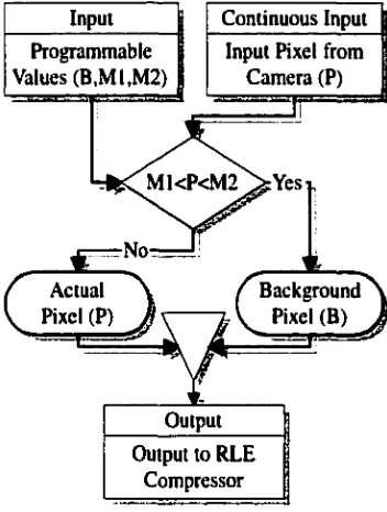
2.7.1 Minimum/Maximum Algorithm
The minimum/maximum algorithm simply replaces any video data which falls between a
specified range with a background value (see Figure 2.15 and Figure 2.16).
Figure 2.15 Graphical Interpretation of the Minimum/Maximum Algorithm
Before RT Processing
B
After RT Processing
University o f Windsor
Figure 2.16 Detailed Flowchart of the Minimum/Maximum Algorithm
Continuous Input
Programmable Values (B,M1,M2)
Input Pixel from Cam era (P)
I
M1<P<M2
Actual Pixel (P)
Background Pixel (B)
I
Output to RLE Compressor
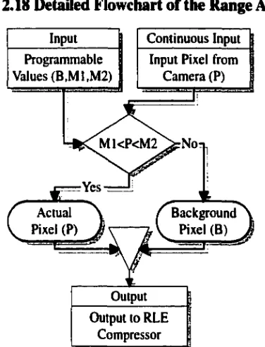
2.7.2 Range Algorithm
The range algorithm is simply the complement of the minimum/maximum algorithm. Any
video data which does not fall between a specified range with be replaced with a
background value (see Figure 2.17 and Figure 2.18).
Figure 2.17 Graphical Interpretation of the Range Algorithm
Before RT Processing
B
After RT Processing
First Generation System Video Data Processing
University o f Windsor
Figure 2.18 Detailed Flowchart of the Range Algorithm
Input I Continuous Input
Programm able 1
Values (B.M 1.M 2) |
Input Pixel from C am era (P)
M1<P<M2 > N o
w " --- i
(
Pixel (P) J y Actual yf
B a c k g r o u n d ^Pixel (B) J OutputOutput to RLE Compressor
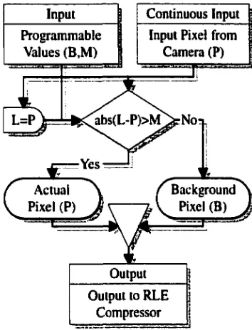
2.7.3 Delta Threshold Algorithm
The delta threshold algorithm calculates the absolute slope between two adjacent values
and replaces the second with the background value if that slope is lower than specified (see
Figure 2.19 and Figure 2.20).
Figure 2.19 Graphical Interpretation of the Delta Threshold Algorithm
Defective if absolute slope is greater than M Before RT Processing
B
After RT Processing
University o f W indsor
Figure 2.20 Detailed Flowchart of the Delta Threshold Algorithm
Input Continuous Input jj
Program m able Input Pixel from 1
Values (B,M ) Camera (P) 1
• “ , T---I
l=p\ = !=*5sC abs(L -P )> M ^rN o*
Actual Pixel (P)
Background Pixel (B)
Output to RLE Com pressor
2.7.4 Delta Tracker
The delta trackers algorithm operates by tracking the background based on the fluctuations
of the incoming values. The pixel value is replaced with the background value when it is
within a specified tolerance (see Figure 2.21 and Figure 2.22).
Figure 2.21 Graphical Interpretation of the Delta Tracker Algorithm
Before RT Processing
B
After RT Processing
First Generation System Video Data Processing 24
University o f Windsor
Figure 2.22 Detailed Flowchart of the Delta Tracker Algorithm
Input
Programmable Values (B.T.W)
Continuous Input
Input Pixel from Cam era (P)
r
te C L -T < P < L + T > Y e s
/ B a c
VJ2
Background Pixel (B)
C=C-1
(
Actual P ixel(P ) \J
P > L ,C=C+1 1
< c = w j >
Yes w.
c = o 1
L=L+1
ft T 2 W
L=L-1 Ur ...- ! i . .
Output
Beginning o f Line g Output to RLE
Com pressor
L=P & C=0 g
2.8
Data Compression
After the FPGA performs its selective pixel elimination, the new data is sent to the
microcontroller which then transmits it to the host. This data must be as compressed as
possible since the transmission speed to the host is slow relative to that o f the camera bus.
At best case, the FPGA algorithm would eliminate all pixels in a line from being defects,
therefore this case should transmit the minimal amount o f data. Since the FPGA is
operating in real time, a data compression scheme must be designed which will compress
the data efficiently and use very little resources.
University o f Windsor
2.8.1 Run-Length Encoding (RLE) Compression
RLE compression is a very simple approach to data compression. It compresses best when
there is a long sequence of duplicate bytes; however, continuous non-repeating bytes cause
non-optimal compression. Although the RLE algorithm differs from one implementation
to another, the concept remains the same. A compressed stream consists of a series of
packets, where each packet begins with a header byte and followed by variable data from 1
to 128 bytes (see Figure 2.23).
Figure 2.23 Decomposition of the Compressed Stream
H eader byte
Variable byte(s) forejim o f G mprt ssed Packet^
Repeat Packet
length
Bytes to be repeated or copied
The header byte (separated into a repeat bit and a 7 bit counter value starting at 0)
represents the type of packet and the amount of data remaining in the packet. When the
repeat bit is set, the counter value contains the number of times the next byte is repeated;
This packet is always 2 bytes. The other packet possibility is when the repeat bit is cleared
and the counter value contains the number o f bytes remaining in the packet to be copied
into the uncompressed stream. See Table 2.4 for some RLE compressed data examples.
Table 2.4 Examples of RLE Compressed Byte Streams
Uncompressed Data
Compressed Packet
25252525252525252525 8925
010304060810 05010304060810
8080808080807F7E80818080808080 8580037F7E80818480
101112131415161718191A1B1C1D 0D101112131415161718191A1B1C1D
Fust Generation System Data Compression 26
University ofW indsor
2.8.2 Real Time RLE Implementation
Although the RLE compression scheme is relatively simple to implement in software, it is
much more difficult to implement in real time hardware. In order to implement the non-
repetitive portion of the compressor, a large buffer is needed to store the outgoing stream
before the header byte. Potential problems involving throughput and buffer overwriting are
very likely, particularly when the compressed stream is being transmitted while new data
is being processed. Instead o f designing around these problems, a modified RLE
compression scheme is introduced.
2.8.3 Modified RLE Compression
The target hardware for the RLE compressor is an FPGA where buffer space or RAM is
very costly in terms of resources. To resolve this, the compressor repeat mode is always
considered on, thus increasing the counter value to 8 bits. This approach effectively
decreases the compression ratio for non-repeating data such that 2 bytes of compressed
data represents one byte of uncompressed data. Although this modification does not
produce the same level o f compression for non-repeating data as the original method, it is
implementable with limited hardware.
Defects and Non-Defects
In order to describe a defect in the compressed data stream, the luminance value obtained
from the camera is encoded with no modifications. However, a non-defect is replaced by a
programmable background value. This background value should be set based on the
requirements of the software algorithms in the host monitoring system which will later
process the compressed stream. Ideally, the compressed low bandwidth data will recreate
the image originally obtained from the camera with only the defects visible.
University o f Windsor
Enhanced Size Encoding
Using the RLE compression method, as described above, we obtain non-optimal results on
long streams o f repetitive data. This will most likely occur when encoding long
background lines (as shown in Figure 2.24).
Figure 2.24 Compressed Single BLACK Line
FFOOFFOOFFOOFFOOO
4
OOTo increase the compression performance of the encoder for these particular instances, a
special header code OxFF is added and the maximum counter value is reduced from 2SS to
2S4 to compensate. This code allows data to be repeated in large streams without having to
re-encode the repeating value (see Figure 2.25). This new code can reduce a compressed
long line by 4 bytes.
Figure 2.25 Compressed Single BLACK Line Using Enhanced Size Encoding
FF00FFFFFF08
Line Synchronization
With RS-232 transmission, there exists the possibility that the host may incorrectly receive
the encoded stream and the decompressor will misinterpret it, losing synchronization with
the beginning of the compressed packets (as seen in Figure 2.26).
Figure 2.26 Example of Possible Transmission Corruption
Normal Stream
Corrupted Stream
FFOOFFFFFFO
8
FFOOFFFFFFO8
FF00FFFF8B08FF00FFFFFF08To avoid this possibility, two OxOO’s are added to the encoded stream (synchronization
command) before the beginning o f a scan line (see Figure 2.27). It is not necessary to
have a synchronization command at every line, in fact in the implemented compressor,
Fust Generation System Data Compression 28
University o f Windsor
synchronization is transmitted every 64 lines without any noticeable failure in the
decompressor.
Figure 2.27 Example of Synchronization in a Corrupted Transmission
Corrupted Stream
Corrupted Stream with
synchronization
FF00FFFF8B08FF00FFFFFF08 ffuoffffsbosouooffooffffffusuooo
2.9
FPGA Internal FIFO
An internal FPGA implemented FIFO is necessary since there is the possibility the
external FIFO could be busy servicing a read operation while a write operation is
requested. The internal FIFO will hold and postpone the write operations to the external
FIFO until it is idle. The internal FIFO also doubles as a data width converter to
compensate for the RLE data compressor, which may write 8 or 16 bits to the internal
FIFO. This data width is determined by an additional output to the RLE compressor along
with the write request line. The external FIFO itself can only handle 8 bit data widths at
15MHz and the compressor can generate up to 16 bits at 7.3MHz. By adding a tag bit to
the internal FIFO data input, data may enter as a 16 bit value but leave as two 8 bit values
by performing two separate writes to the external FIFO. The internal FIFO is easily
realized by using a special CLB dual port RAM component available only in the Xilinx
4000E series FPGAs [35]. Each dual port RAM is a true 16x1 memory device with edge
triggered control. A 16-bit by 16 deep FIFO is made by connecting 17 of these RAM
components in parallel (as shown in Figure 2.28) and adding logic for pointer control.
The hardware description code for the internal FIFO can be found in Appendix B.2.3
"Main VHDL Code" on page 148.
University o f Windsor
Figure 2.28 Internal FIFO Structure
]
Pointers, Contro
Contro
16 Bit Data In
ir°n
8 Bit Data Out
|
8 Bit Data Out
- I X
Multiplexer
j
8 Bit Data Out
5 J
2.10 FPGA External FIFO
Due to the possibility of large data bursts (continuous defects) from the real-time
processing algorithms inside the FPGA (up to 15MHz assuming two bytes per defect
generated by RLE compressor), the system-to-host transfer rate o f 9600 baud is certainly
too slow to handle reliable transmission without data overrun. Therefore, a simulated
external FIFO is created by a single port SRAM device (128K byte) and additional logic
implemented in the FPGA.
The implementation o f the external FIFO was difficult due to unexpected read timing
problems associated with the particular SRAM device in this system. The SRAM control
lines (WE and OE) are controlled by using multi-phase clocking at the camera clock rate
of 15MHz. A write operation performed within a single cycle (as expected); however, the
read operation did not meet the required one and a half cycle time. The read operations
(with back-to-back write) were not proven reliable until the operation was expanded to
First Generation System FPGA External FIFO 30
University ofW indsor
three clock cycles. See Figure 2.29 for a complete detail on the cycle operation o f the
simulated external FIFO.
Figure 2.29 External FIFO Read/Write/Idle/Reset Operations Flow Diagram
Always Rising Edge
DATA=wdata
W rite Rising Edge /O E = l /WE=1 ADDR=W POINT tri DATA=OUTPUT W POINT++ FSIZE++ EM PTY=false FULL=?
W rite Falling Edge j
/O E = l /W E=0
Read Rising Edge /O E =l /WE=1 ADDR=RPOINT triDATA=INPUT
Read Falling Edge /O E=l /WE=1
Read Rising Edge /OE=0 AVE=1
Read Falling Edge i /OE=0 /W E =l
Read Rising Edge ! /O E=l
/W E=I rdata=DATA
RPOINT++ F S IZ E -EMPTY=? FULL=false
Read Falling Edge /O E=l /WE=1
Idle Rising Edge |j Asynchronous Reset
/O E = l /O E = l
/WE=1 /WE=1
ADDR=W POINT ADDR=WPOINT
Iri DATA=OUTPUT triDATA=OUTPUT
- * WPOINT=0
Idle Falling Edge RPOINT=0
/O E = l FSIZE=0
/WE=1 EMPTY=true
FULL=false
2.11 Hardware Design Tools
2.11.1Synopsys Design Compiler
The Synopsys Design Compiler synthesises VHDL or Verilog code into logical netlists by
instantiating a vast library of elements based on the timing models and design constraints
o f the target hardware. See Appendix B.2.1 "Synopsys Design Compiler Procedure and
Scripts" on page 144 for more information.
University of Windsor
2.11.2 Xilinx XACT
The logical netlist created by Design Compiler is optimized and transformed to the
available components o f the target FPGA. The software performs automatic placement
and routing (if possible) and generates a downloadable bitstream for directly programming
the FPGA. See Appendix B.2.2 "Xilinx Scripts" on page 147 for more information.
2.11.3 Microcontroller Assembler
A freeware mini-assembler provided by Motorola is used to convert text based assembly
code [13] into a special format file structure (S19) which is interpreted by the MCU’s
BUFFALO monitor and the host software. See Appendix B.1.1 "Code Building Utilities"
on page 101 for more information.
2.12 Host Software Design
The target host environment is an IBM compatible PC running the Microsoft Windows NT
4.0 which is a 32-bit protected operating system. In order to interface with the RS-232
hardware reliably at a user level for this application, special software coding styles are
required to interface with the kernel level. A multi-threaded graphical user interface (GUI)
programmed with Microsoft Visual Studio v4 is created (see B.3 "PC Host Software
Code" on page 184) which displays the reconstructed video image from the camera
incoming data stream (see Figure 2.30).
First Generation System Host Software Design 32
University o f Windsor
Figure 2.30 Software Development Environment and Host Monitoring Software
wrvj20«0uQ
BYTE ch*ck_Min[5i=wof (LARCEJ!AGIC)-l ]. BYTE cfaeck_sub(3iz»f (FPCAJUGIC)-U.
l i t 'til e O p e n t tilen A ae. C F ils aodeRoad I C F ile abareOanflfene) )
{
re tu rn FALSE.
CArchive * r( i f l i e . CArchive lo ad ).
/ 3a*-r ju re t i l e v.*ae and v e rsio n a r e c o rre c t a r Raad(chock_aaxa. a izeo f (ch ee k _ M in )).
i t ( s t r n n p t ( c o a s t ch a r • )cbeck_M in. LARCH MAGIC.aizeot(check — ia ) H * 0 )
Ulsl
a r C loset ) f i l e C lo s e t). re tu rn FALSE
a r . Readtcheck^sub. s is e o t (check_at • )chedL t i t (s trn c a p t(c o a s t char
C
a r C lo s e t).
M le.Clnenf)
ffSKtTTvSCTBTvt
T ia e rH itt) w ith 976 byt C aalnt
C aslnt C aalnt C aalat
S topC apturet)
T iaerH itt) w ith 729 b y tes T iaerH itt) w ith 54 b y tes
2.13 Summary
The FPGA realtime video processing algorithms and internal FIFO operate as expected at
the target 7.5MHz data rate and 15MHz clock rate. However, the external FIFO is not
viable in the second generation system since it is unable to be emptied as fast as it can be
filled and it simply consumes to many FPGA resources.
The RS-232 transmission is definitely not capable o f handling the maximum bandwidth of
the processed data from the FPGA video algorithms. The streaming nature and lack of
error correction in RS-232 transmission is difficult to compensate for in this system where
host-camera synchronization is imperative. An inexpensive synchronous high-speed
transmission system which is capable handling network environments with packet
structures is more appropriate for this application.
University o f Windsor
The 68HC11 MCU operates as well as could be expected, however, the 512 byte RAM
limitation causes difficulty in coding complex procedures. If the transmission system were
to be upgraded, the MCU couldn’t handle the additional load. A faster and larger internal
memory MCU device is suggested for the second generation system.
First Generation System Summary 34