ABSTRACT
STEVENS, ERIC CHRISTOPHER. From Novel Processes to Industrially Relevant Applications: Atomic Layer Deposition of Metal, Metal Oxide, and Metal Carbide Thin Films. (Under the direction of Dr. Gregory N. Parsons).
The demand for faster electronic devices with better storage capacity, all without being prohibitively expensive, requires innovations in process design and chemistry. Atomic layer deposition (ALD) is one such process which allows for thin films of material to be deposited with sub-nanometer thickness control. ALD relies on self-limiting chemical reactions, which leads to uniform, pin-hole free, and conformal coatings on substrates with complex and three-dimensional architectures.
We investigated a novel ALD process for the deposition of tin (Sn) metal using a vapor phase reducing agent and a metal halide precursor. This study marked the first thermal (i.e., without plasma) ALD process for elemental Sn, where the mechanism and growth properties as a function of temperature were studied using in situ methods. Sn metal films have a broad range of applications from nanowire transistors to anode materials for lithium ion batteries.
In a similar fashion, we also studied the use of a novel ALD precursor, tungsten (V) chloride, to deposit tungsten carbide (WC) thin films, using trimethyl aluminum as a co-reagent. In situ studies revealed key information regarding the likely reaction pathways as well as saturation behavior at different temperatures. The deposited WC films were doped with aluminum and had low Cl impurities. WC films have many applications in the semiconductor industry due to their chemical stability, hardness, and high conductivity.
growth of titanium oxide (TiO2), hafnium oxide (HfO2), and titanium nitride (TiN) was observed. The use of a hydrogen plasma pretreatment on aC removed oxygen species and passivated the surface with C-H groups, leading to a nucleation delay for TiO2, HfO2, and TiN. We showed that the use of water as a co-reagent in metal oxide ALD leads to significant nucleation site generation, while the ammonia co-reagent in TiN ALD resulted in enhanced selectivity.
We applied two different models to describe the nucleation behavior of metal oxide and metal nitride ALD on plasma-treated aC. The best fit of the experimental data was obtained using a modification based on the Avrami Equation, which assumed random dispersion of nucleation sites on the surface increasing at some rate. The insights gained from the model fit show that water plays a key role in the generation of new nucleation sites for metal oxide ALD. This model can be applied to other ALD processes to gain valuable information regarding the nucleation behavior as well as potential selectivity losses.
From Novel Processes to Industry-Relevant Applications: Atomic Layer Deposition of Metal, Metal Oxide, and Metal Carbide Thin-Films.
by
Eric Christopher Stevens
A dissertation submitted to the Graduate Faculty of North Carolina State University
in partial fulfillment of the requirements for the degree of
Doctor of Philosophy
Chemical Engineering
Raleigh, North Carolina 2018
APPROVED BY:
_______________________________ _______________________________ Dr. Gregory N. Parsons Dr. Michael D. Dickey
Committee Chair
ii DEDICATION
iii BIOGRAPHY
Eric Stevens was born and raised in Phoenix, AZ, to Chuck and Margaret Stevens. Eric attended Arizona State University (Go Devils) in Tempe, AZ, where he studied chemical engineering. Eric gained valuable research experience under the mentorship of Professor Lenore Dai, where he worked on the integration of silicon ribbons with stimuli responsive hydrogels. While at Arizona State, Eric was a teaching assistant for lower and upper division chemical engineering courses, as well as a tutor for organic chemistry. Eric decided to pursue graduate school following the completion of an internship at Pacific Northwest National Laboratory. Under the direction of Dr. Carlos Fraga, Eric designed and implemented a novel, chemical forensic technique to identify trace impurities in chemical warfare agents and establish a direct link to the respective manufacturer using two-dimensional gas chromatography/time-of-flight mass spectrometry.
In Fall 2013, Eric began his Ph.D. in chemical engineering under the direction of Professor Gregory Parsons at North Carolina State University in Raleigh, NC. Eric’s research was mainly focused on development of new atomic layer deposition processes for deposition of metal and metal carbide thin films. Eric continued his studies at IMEC in Leuven, Belgium, under the mentorship of Professor Annelies Delabie. At IMEC, Eric studied the use of atomic layer deposition for advanced patterning applications relevant to the semiconductor industry. Eric will join the Research and Development team at ASM America in Phoenix, AZ, after graduation.
iv ACKNOWLEDGMENTS
To my advisor Professor Gregory Parsons, thank you for your guidance and support throughout this process. You have molded me into a researcher and scientist, constantly encouraging me to find answers to challenging problems. Thank you for sticking by me through everything and helping me with a slight nudge here and a carefully crafted “…” in your emails. I am honored to be one of your students and future colleague in the ALD community.
To Professor Annelies Delabie, thank you for giving me the opportunity to conduct research at IMEC. That experience was both challenging and gezellig (did I use this in the correct context?), and one that had a profound impact on my future and for that I am extremely grateful to you and entire team at IMEC, including Yoann, BT, Efrain, Sven, and Elie. Dank u wel voor alles! To Professor Lenore Dai, thank you for your support and guidance during my time at ASU. You helped me tremendously along the way, without you I wouldn’t have likely pursued graduate school.
To Mr. Mariner, thank you for piquing my interest in chemistry and steering me towards a major in Chemical Engineering. You gave me a passion for teaching and I aim to make STEM outreach a major part of my life going forward. With regards to breaking things and setting them on fire… you also gave me that passion as well.
A special thanks to my fellow classmates and friends at NC State: Wenyi, Jenny, Mariah, Jason, Adam, Ryan, and Ishan. It has been a long journey, but we finally made it. All the long nights working on transport and perturbation theory were well worth it in the end!
v of the sacrifices you made for my future. I hope to be half the person you both are in the future. Thank you and I love both you so much.
To the rest of my family, Matt, Lauren, Shawn, Gina, Daniel, Jim, and Lisa, thank you for your love and support through this, and for all the less than exciting conversations you all endured regarding my research. Although I am the youngest of the three brothers, I feel that I am the favorite. I wanted that to be in writing for future generations to know. Joking aside, your support has no bounds and for that I am grateful. Love you guys.
vi TABLE OF CONTENTS
LIST OF TABLES ... xiii
LIST OF FIGURES ... xiv
Chapter 1: Introduction and Background ... 1
1.1 Atomic Layer Deposition Background and Applications ... 2
1.2 Basic Principles of Atomic Layer Deposition ... 3
1.2.1 Surface Reactions in Atomic Layer Deposition ... 3
1.2.2 Thermodynamics of Atomic Layer Deposition ... 4
1.2.3 Growth Rate Versus Temperature ... 5
1.2.4 Nucleation and Growth Modes ... 5
1.3 Materials Deposited Using Atomic Layer Deposition ... 6
1.3.1 Atomic Layer Deposition of Metal Oxides ... 6
1.3.2 Atomic Layer Deposition of Metals ... 7
1.3.3 Atomic Layer Deposition of Metal Carbides ... 8
1.4 Area-Selective Atomic Layer Deposition ... 9
1.5 Figures for Chapter 1 ... 11
1.6 References ... 15
Chapter 2: Thermal Atomic Layer Deposition of Sn Metal Using SnCl4 and a Vapor Phase Silyl Dihydropyrazine Reducing Agent ... 27
2.1 Abstract ... 28
2.2 Introduction ... 29
2.3 Experimental ... 30
vii
2.3.2 ALD Precursors and Delivery ... 31
2.3.3 Substrate Preparation ... 32
2.3.4 In situ Characterization ... 33
2.3.5 Ex situ Characterization ... 34
2.4 Results ... 35
2.4.1 Quartz Crystal Microbalance ... 35
2.4.2 Growth Rate on QCM Substrates ... 37
2.4.3 Film Morphology on QCM and Si Substrates ... 38
2.4.4 Film Composition ... 39
2.4.4.1 ToF-SIMS Depth Profiling ... 39
2.4.4.2 XPS Depth Profiling ... 40
2.4.5 In situ Reaction Monitoring by Quadrupole Mass Spectrometry ... 41
2.4.5.1 Characteristic Mass Fragments of Unreacted SnCl4 and DHP ... 41
2.4.5.2 In situ Reaction Analysis during SnCl4/DHP Processing ... 42
2.5 Discussion ... 43
2.5.1 Proposed SnCl4/DHP Reaction Mechanism ... 43
2.5.1.1 SnCl4 Adsorption ... 43
2.5.1.2 DHP Desilylation and Pyrazine Elimination ... 44
2.5.2 Growth Saturation ... 45
2.5.3 Film Composition ... 47
2.6 Conclusions ... 48
2.7 Acknowledgements ... 49
viii
2.9 Tables for Chapter 2... 61
2.10 References ... 62
Chapter 3: Thermal Atomic Layer Deposition of Tungsten Carbide by WCl5 and Trimethyl Aluminum ... 66
3.1 Abstract ... 67
3.2 Introduction ... 67
3.3 Experimental ... 68
3.3.1 ALD Reactor Setup ... 68
3.3.2 ALD Precursors and Delivery ... 69
3.3.3 Substrate Preparation and in situ QCM ... 69
3.3.4 Ex situ Characterization ... 70
3.4 Results ... 71
3.4.1 Temperature Dependence and on Film Growth by QCM ... 71
3.4.2 Dose Saturation ... 72
3.4.3 Growth Rate from QCM ... 73
3.4.4 Film Composition ... 74
3.4.5 Thermodynamic Modeling... 76
3.5 Discussion ... 76
3.6 Conclusions ... 79
3.7 Acknowledgements ... 80
3.8 Figures for Chapter 3 ... 81
3.9 Tables for Chapter 3... 90
ix Chapter 4: Growth Inhibition of TiN, TiO2, and HfO2 on Plasma-Treated Amorphous
Carbon by Area-Selective Atomic Layer Deposition ... 97
4.1 Abstract ... 98
4.2 Introduction ... 99
4.3 Experimental ... 101
4.3.1 Substrate Preparation, Plasma and ALD Processing ... 101
4.3.2 Characterization ... 102
4.4 Results and Discussion ... 103
4.4.1 ALD on Untreated aC Substrates ... 103
4.4.2 aC Surface Composition and Modification Using Plasma Exposures ... 104
4.4.3 Optimization of H2 Plasma Conditions ... 106
4.4.4 Nucleation and Growth of TiO2, HfO2, and TiN ALD on Plasma-Treated aC and Si3N4 Substrates ... 108
4.4.5 Selectivity Loss of Plasma-Treated Carbon ... 111
4.5 Conclusions ... 112
4.6 Acknowledgements ... 113
4.7 Figures for Chapter 4 ... 114
4.8 Tables for Chapter 4... 123
4.9 References ... 125
Chapter 5: Modeling the Nucleation of TiO2, HfO2 and TiN Atomic Layer Deposition on Plasma-Treated Amorphous Carbon ... 129
5.1 Abstract ... 130
x
5.3 Experimental ... 132
5.3.1 aC Substrate Preparation ... 132
5.3.2 Atomic Layer Deposition and H2 Plasma Processing ... 132
5.3.3 Characterization ... 133
5.3.4 Models... 134
5.3.4.1 Island Growth Model ... 134
5.3.4.2 Modified Island Growth Model - Avrami Equation ... 135
5.4 Results and Discussion ... 137
5.4.1 Particle Analysis from SEM ... 137
5.4.2 Island Growth Model ... 139
5.4.3 Modified Island Growth Model - Avrami Equation ... 141
5.5 Conclusions ... 144
5.6 Acknowledgements ... 144
5.7 Figures for Chapter 5 ... 145
5.8 Tables for Chapter 5... 160
5.9 References ... 162
Chapter 6: Area-Selective Atomic Layer Deposition of TiN and TiO2 in Sub-50 nm aC/Si3N4 Patterns for Advanced Patterning Applications ... 165
6.1 Abstract ... 166
6.2 Introduction ... 166
6.3 Experimental ... 168
6.3.1 Materials, Plasma, and ALD Processing... 168
xi
6.3.3 Characterization ... 170
6.4 Results and Discussion ... 170
6.4.1 Formation and Plasma Treatment Processing of Sub-50 nm aC/Si3N4 Patterned Structures ... 170
6.4.2 TiO2 and TiN ALD for Bottom-Up Fill in Sub-50nm aC/Si3N4 Patterned Structures ... 172
6.4.2.1 Film Thickness and Growth Per Cycle ... 172
6.4.2.2 Angle-Resolved XPS to Assess Selectivity ... 173
6.4.2.3 Nucleation Differences for Pattern vs. Blanket Substrates ... 174
6.4.2.4 Tone Reversal by Selective aC Removal ... 174
6.5 Conclusions ... 175
6.6 Acknowledgements ... 176
6.7 Figures for Chapter 6 ... 177
6.8 Tables for Chapter 6... 185
6.9 References ... 186
Appendices ... 190
Appendix A1: Thermal Chemical Vapor Etch Selectivity of TiO2 versus Al2O3 Using Vapor Phase WCl5 ... 191
A1.1 Experimental ... 192
A1.1.1 ALD Precursors and Delivery ... 192
A1.1.2 In situ QCM ... 193
A1.2 Results and Discussion... 193
xii
A1.4 References ... 202
Appendix A2: In Situ Study of Titanium Carbide by Thermal ALD ... 203
A2.1 Experimental ... 204
A2.1.1 ALD Precursors and Delivery ... 204
A2.1.2 In situ QCM ... 205
A2.2 Results and Discussion... 205
A2.3 Figures for Appendix A2 ... 209
xiii LIST OF TABLES
Table 2.1 Film Impurity Content from XPS Analysis vs. Deposition Temperature. ... 61
Table 3.1 GPC from Average Mass Change during WCl5/TMA for ρ(α-WC)=15.6 g/cm3. ... 90
Table 3.2 GPC from Average Mass Change during WCl5/TMA for ρ(α-W2C)=16.6 g/cm3 ... 91
Table 3.3 Mass Ratio vs. WCl5/TMA Reaction Pathway... 92
Table 4.1 TiO2, HfO2, and TiN Bulk Film Properties. ... 123
Table 4.2 C 1s Peak Deconvolution for Plasma Treated aC. ... 124
Table 5.1 Island Growth Model Parameters for TiO2, HfO2, and TiN ALD ... 160
Table 5.2 Modified Island Growth Model Parameters for TiO2, HfO2, and TiN ALD ... 161
xiv LIST OF FIGURES
Figure 1.1 Schematic of Al2O3 by ALD using Al(CH3)3 and H2O precursors. Exposure of a reactive substrate (-OH groups) to Al(CH3)3 will result in a complete reaction of all available surface sites, giving off CH4 byproducts and forming Al-O bonds. After purging excess reactant and byproducts using inert gas, H2O can be exposed to the newly terminated surface (Al-CH3), releasing CH4 byproducts. Following another purge step, this process can be repeated in a cyclic manner until the desired film thickness is reached. ... 11 Figure 1.2 Quantum chemical calculations of the anticipated reaction pathways and
associated energetics during the reaction of Al(CH3)3 + H2O. a) shows the first half-reaction of gas-phase Al(CH3)3 reacting with Al-OH* surface sites. b) shows the second half-reaction of gas-phase H2O with Al-(CH3)* surface sites. Figure reproduced from Ref 54 ... 12 Figure 1.3 Growth rate as a function of deposition temperature for ALD processing. For
most ALD processes, there exists an ALD window, which is a range of
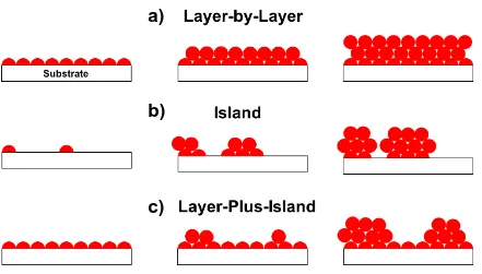
temperatures where the film growth rate is constant. Outside of this window, the growth can vary depending on the temperature and specific reaction chemistry ... 13 Figure 1.4 Schematic of the three growth modes typically observed during ALD: a)
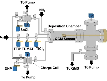
layer-by-layer (Frank-van der Merwe), b) island (Volmer-Weber), and c) layer-plus-island (Stranski-Krastanov) growth ... 14 Figure 2.1 Homemade, hot wall ALD reactor with direct-port and charge cell precursor
delivery. N2 carrier and purge gas was used, with an operating pressure of 1.5 Torr. In situ QCM and QMS capabilities were used to monitor the mass uptake and reaction byproducts, respectively, during ALD processing... 50 Figure 2.2 Mass change, measured by QCM, as a function of deposition time during
SnCl4/N2/DHP/N2 (2s/40s/2s/40s) processing at a) 130 oC for 650 cycles and b) 170 oC for 500 cycles. Depositions were carried out on as-received Au-coated QCM crystals. Inset graphs show 3 cycles of SnCl4/N2/DHP/N2 within linear
xv Figure 2.3 a) Mass change vs. deposition time, obtained by in situ QCM, during multiple
consecutive SnCl4/DHP exposures as a function of the deposition temperature, 150 (top, black line) and 210 oC (bottom, red line). b) Magnified region from a) to show sub-dose behavior. Solid arrows indicate the instance of 2 second SnCl4 and DHP doses, separated by 100 and 200 second N2 purges for depositions
carried out at 150 and 210 oC, respectively ... 52 Figure 2.4 Mass change, obtained by QCM, showing the average mass uptake per cycle
obtained during SnCl4/DHP depositions at 130, 150, 170, 190, 210 oC. The reported mass change is an average of the values obtained with saturated
consecutive exposures, at a given temperature ... 53 Figure 2.5 Top-down SEM images of a) as-received Au-coated QCM crystal, b) 1000
cycles of SnCl4/DHP deposited at 150 oC on Au-coated QCM crystal, c) 1000 cycles of SnCl4/DHP deposited at 190 oC on Au-coated QCM crystal. Scale bars 2 µm. ... 54 Figure 2.6 a) Cross-sectional SEM image of the Si-H/Sn/TiN/TiO2 sample deposited at 190
oC (1500 cycles SnCl4/DHP, 1300 cycles TDMAT/NH3, 1500 cycles
TTiP/TiCl4) and cut using a Focused Ion Beam. The platinum bar was used to protective the area of interest during ion milling. Sn films show good thickness uniformity over the micron length scales. b) Magnified SEM image of a). The average thickness of the Sn layer was 41 + 1 nm and the total capping layer
thickness was 129 + 2 nm. ... 55 Figure 2.7 a) ToF-SIMS results of the Si-H/Sn/TiN/TiO2 sample used for FIB SEM.
Layers were labeled and color coded as follows: “Capping Layer TiO2 and TiN” – yellow, “Sn” – grey, “Si” – purple. The ions tracked for the capping layer were TiO2- (orange), O2- (red), 37Cl- (teal), and CN- (pink). The Sn- (grey), SiO2 -(green), and SnO2- (blue) were used to identify the Sn region. b) O, C, N, and Cl impurities within the Sn region... ... 56 Figure 2.8 a) XPS survey scans of the Si-H/Sn/TiN/TiO2 stack deposited at 190°C, with
xvi minutes of sputtering (red line), the Sn 3d peaks between 500 - 480 eV start to increase in intensity. A maximum in the Sn 3d peak intensity most likely occurs between 125 – 159 minutes of sputtering. After 159 minutes of sputtering, the Sn 3d peak intensity decreases accompanied with a rise Si 2p peak intensity, indicative of the underlying Si substrate. b) High resolution scans of the Sn 3d 5/2 region showing Sn-Sn (485 eV) and Sn-O (486.7 eV) chemical bonds as a function of Ar sputter time of the same samples in a). Spectra offset for visual clarity ... 57 Figure 2.9 Analog mass spectrometry scans from direct sampling of each individual charge
cell (maintained at 120 oC), and thus the unreacted SnCl4 and DHP species. a) SnCl4 mass fragmentation patterns for 50 consecutive doses, separated by N2 purges. Most prominent peak observed at m/z = 224, with predicted structure of the SnCl4 mass fragment shown. b) DHP mass fragmentation patterns for 50 consecutive doses, separated by N2 purges. Most prominent peak observed at
m/z = 146, with predicted structure of the DHP mass fragment shown. ... 58 Figure 2.10 QMS data during SnCl4/DHP processing at 190 oC on Si substrates for 5
sub-doses of SnCl4 followed by 5 sub-sub-doses of DHP, separated by N2 purges. Most prominent mass fragments a) m/z 224 (black) and b) 146 (green) shown with their respective predicted structures. c) SnCl4/DHP dosing sequence
corresponding to the QMS data in a) and b) ... 59 Figure 2.11 Proposed reaction mechanism between DHP and two surface-bound SnClx
species. 1) SnCl4 exposure and subsequent densification gives a Sn–Cl surface. 2) DHP is exposed to the Sn–Cl surface, breaking Si–N bonds on the DHP to give off TMS-Cl byproducts. 3) Intermediate ring structure which can donate electrons to create a Sn-Sn bond and eliminate pyrazine. 4) One Sn–Sn bond
formed per DHP molecule ... 60 Figure 3.1 QCM results showing the mass change (ng/cm2) versus process time (minutes)
for a) 100 cycles of WCl5/N2/TMA/N2, with dose times 1s/30s/1s/30s, at 150 oC and b) 50 cycles [WCl5/N2]×5/[TMA/N2]×5, with dose times
xvii respectively, showing 3 cycles, with WCl5 and TMA doses indicated with
arrows. ... 81 Figure 3.2 QCM results showing the mass change (ng/cm2) versus process time (minutes)
for a) 100 cycles of WCl5/N2/TMA/N2, with dose times 1s/30s/1s/30s, at 300 oC and b) 100 cycles [WCl5/N2]×5/[TMA/N2]×5, with dose times
[1s/30s]×5/[1s/30s]×5, at 300 oC. c) and d) are magnified images of a) and b), respectively, showing 3 cycles, with WCl5 and TMA doses indicated with
arrows ... 82 Figure 3.3 Average mass change per cycle (ng/cm2/cycle), obtained from QCM results,
versus deposition temperatures 150, 200, 250, 300, and 325 oC for
WCl5/N2/TMA/N2 (black squares) and [WCl5/N2]×5/[TMA/N2]×5 (red circles). ... 83 Figure 3.4 WCl5/TMA ratio (y-axis) of the averaged mass change obtained by QCM during
WCl5 and TMA cycling. The number of WCl5 (1, 3, 5 on x-axis) and TMA (1– black squares, 3–red circles, 5–blue triangles) sub-doses were varied for deposition temperatures of a) 150 oC, b) 200 oC, c) 250 oC, d) 300 oC, and e)
325 oC ... 84 Figure 3.5 Elemental depth profile, obtained using XPS with Ar sputtering, for a) 200
cycles of [WCl5/N2]×2/[TMA/N2]×2 at 200 oC and b) 400 cycles of
[WCl5/N2]×2/[TMA/N2]×2 at 300 oC deposited on Si with native oxide. Species shown, with units of atomic percent, are: W (blue triangles), O (black squares), C (red circles), Al (pink upside-down triangles), Cl (green diamonds), and Si
(navy blue left-triangles) ... 85 Figure 3.6 High resolution scans of the W 4f region, obtained using XPS with Ar
sputtering (representative sputtering times indicated above each designated line), for a) 200 cycles of [WCl5/N2]×2/[TMA/N2]×2 at 200 oC, and b) 400 cycles of [WCl5/N2]×2/[TMA/N2]×2 at 300 oC deposited on Si with native oxide. Raw spectra offset for visual clarity. Expected peaks for WO3 doublet at ~36 and 38 eV and WCx doublet at ~32 and 34 eV are indicated above raw
xviii Figure 3.7 High resolution scans of the C 1s region, obtained using XPS with Ar sputtering
(representative sputtering times indicated above each designated line), for a) 200 cycles of [WCl5/N2]×2/[TMA/N2]×2 at 200 oC, and b) 400 cycles of [WCl5/N2]×2/[TMA/N2]×2 at 300 oC deposited on Si with native oxide. Raw spectra offset for visual clarity. Expected peaks for C─C, W─C, and Al─C bonding at ~284., ~283.5, and 282.2 eV, respectively, are indicated above raw spectra. ... 87 Figure 3.8 High resolution scans of the Al 2p region, obtained using XPS with Ar
sputtering (representative sputtering times indicated above each designated line), for a) 200 cycles of [WCl5/N2]×2/[TMA/N2]×2 at 200 oC, and b) 400 cycles of [WCl5/N2]×2/[TMA/N2]×2 at 300 oC deposited on Si with native oxide. Raw spectra offset for visual clarity. Expected peaks for Al─O and Al─C bonding at ~75 and ~73.5 eV, respectively, are indicated above raw spectra ... 88 Figure 3.9 Predicted equilibrium species from the gas phase reaction of 1 mole of WCl5
and 1.5 moles of Al(CH3)3 from temperatures ranging 25 – 400 oC and pressure of 2 mbar. Only species with an equilibrium concentration greater than 1 mmol are shown. The following are the species expected at equilibrium, with their anticipated phase indicated as either (g) for gas or (s) for solid, CH4(g) (black), AlCl3(g) (red), WC(s) (blue), AlCl3(s) (pink), Al2Cl6 (green), and HCl(g)
(orange)... 89 Figure 4.1 Ti and Hf content, measured by RBS, for TiO2 (blue circles), HfO2 (red
triangles), and TiN (black squares) ALD films deposited on untreated aC
(closed shapes) and Si3N4 (open shapes) versus the number of ALD cycles. ... 114 Figure 4.2 Oxygen concentration determined by XPS depth profiling of 100 nm aC films
deposited on Si wafers. Untreated aC sample (green upside-down triangles) represents as-deposited films with no plasma processing. aC films were treated with hydrogen plasma for 100W 50s (black triangles), 200W 50s (red
diamonds), and 400W 50s (blue circles) ... 115 Figure 4.3 High resolution XPS scans of the C 1s region for untreated aC (black line),
xix line), and the same 400W 50s treated aC sample measured after 1 week of air
exposure. C–C, C–O, and C=O bonding types can be ascribed to peak energies of 284 – 285, 286, and 288 eV, respectively. C–C sp2 and sp3 bonding
hybridization was indicated at 284 and 285 eV, respectively. ... 116 Figure 4.4 a) Resulting content of Ti (by RBS) on aC substrates for 50 (orange square),
100 (black triangles), 200 (red diamonds), and 400W (blue circles) plasma power for 10, 50, and 100s exposure times followed by 30 cycles of TiO2 ALD at 250oC. A 0W (green triangle) treatment represents untreated aC when no plasma was used, thus serving as the control sample. The RBS detection limit for Ti was determined to be ~8×10¹³ at/cm2 for the tool ... 117 Figure 4.5 Ti or Hf content from RBS, in units of atoms/cm2, obtained after ALD growth
on untreated aC (black squares), plasma-treated Si3N4 (blue triangles), and plasma-treated aC (red circles) substrates for a) TiO2 by Ti(OCH3)4/H2O at
250oC b) HfO2 by HfCl4/H2O at 300oC c) TiN by TiCl4/NH3 at 390oC... 118 Figure 4.6 Top-down SEM images obtained for ALD a) TiO2, b) HfO2, c) TiN films for
various numbers of cycles after plasma treatment on aC blanket substrates. All scale bars are 100 nm ... 119 Figure 4.7 a) Particle density (1/cm2) and b) nuclei areal surface coverage (from SEM
image analysis) as a function of the amount of material deposited (obtained from RBS measurements) for HfO2 (red squares), TiO2 (black squares), and TiN (blue triangles) on 400W 20s H2 plasma-treated aC. The corresponding number of cycles for the particle density and areal coverage of TiO2 and HfO2, from left to right, are 20, 30, 60, 90, 120, and 200 cycles. Similarly, the corresponding
number of cycles for TiN, from left to right, are 200, 320, 480, 640 cycles ... 120 Figure 4.8 Top down SEM images of plasma-treated aC blanket substrates with a) 0, b) 1,
c) 10, and d) 20 2s H2O exposures (with 4s Ar purges) at 250oC followed by
150 cycles of TiN ALD. Scale bars 100 nm. ... 121 Figure 4.9 a) Particle density (1/cm2) and b) nuclei areal surface coverage as a function of
xx 20s H2 plasma-treated aC. Plasma treated aC substrates subjected to 1, 10, and
20 H2O water exposures (2s dose, 4s Ar purge) followed by 150 cycles of TiN ALD (open blue triangles). Plasma-treated aC substrates not subjected to H2O, with 200 and 320 cy TiN ALD are also given for reference (closed blue
triangles) ... 122 Figure 5.1 Top down SEM images of TiO2 particles on plasma-treated aC substrates
subjected to a) 30, b) 60, c) 90, d) 120, and e) 200 cycles of Ti(OCH3)4 + H2O at 250 oC. Included under each SEM image are overlaid particle outlines (shown in green) generated from particle analysis in ImageJ. All scale bars are 50 nm ... 145 Figure 5.2 Top down SEM images of HfO2 particles on plasma-treated aC substrates
subjected to a) 30, b) 60, c) 90, d) 120, and e) 200 cycles of HfCl4 + H2O at 300 oC. Included under each SEM image are overlaid particle outlines (shown in
green) generated from particle analysis in ImageJ. All scale bars are 50 nm. ... 146 Figure 5.3 Top down SEM images of TiN particles on plasma-treated aC substrates
subjected to a) 200, b) 320, c) 480, and d) 640 cycles of TiCl4 + NH3 at 390 oC. Included under each SEM image are overlaid particle outlines (shown in green) generated from particle analysis in ImageJ. All scale bars are 50 nm ... 147 Figure 5.4 Areal surface coverage of identified a) TiO2 and HfO2, and b) TiN particles
from top-down SEM images in Figures 5.1 (TiO2), 5.2 (HfO2), and 5.3 (TiN) ... 148 Figure 5.5 TiO2 particle size distributions, calculated using ImageJ, given as particle count
versus radius on plasma-treated aC substrates for 30 (black), 60 (red), 90 (blue), and 120 (green) cycles of Ti(OCH3)4 + H2O at 250 oC. Total particle counts were normalized over an area of 1 cm2. The theoretical particle radius (rn*), indicated using a vertical line at the expected radius, was estimated assuming a growth per cycle of 0.043 nm/cy (from spectroscopic ellipsometry
measurements) ... 149 Figure 5.6 HfO2 particle size distributions, calculated using ImageJ, given as particle count
xxi normalized over an area of 1 cm2. The theoretical particle radius (rn*), indicated using a vertical line at the expected radius, was estimated assuming a growth
per cycle of 0.05 nm/cy (from spectroscopic ellipsometry measurements). ... 150 Figure 5.7 TiN particle size distributions, calculated using ImageJ, given as particle count
versus radius on plasma-treated aC substrates for 200 (black), 320 (red), 480 (blue), and 640 (green) cycles of TiCl4 + NH3 at 390 oC. Total particle counts were normalized over an area of 1 cm2. The theoretical particle radius (rn*), indicated using a vertical line at the expected radius, was estimated assuming a growth per cycle of 0.031 nm/cy (from spectroscopic ellipsometry
measurements). ... 151 Figure 5.8 TiO2 island surface fraction as a function of ALD cycling on plasma-treated aC.
Black squares are areal coverage of TiO2 islands calculated from SEM images in Figure 5.1, while the dotted and dashed lines correspond to the resulting fit using the Island Growth Model with layer closure parameter, nc, equal to 150
and 180 cycles, respectively. ... 152 Figure 5.9 HfO2 island surface fraction as a function of ALD cycling on plasma-treated aC.
Black circles are data points from areal coverage of HfO2 islands calculated from SEM images in Figure 5.2, while the dotted, dot-dashed, and dashed lines correspond to the resulting fit using the Island Growth Model with layer closure parameter, nc, equal to 100, 120, and 150 cycles, respectively ... 153 Figure 5.10 TiN island surface fraction as a function of ALD cycling on plasma-treated aC.
Black triangles are data points from areal coverage of TiN islands calculated from SEM images in Figure 5.3, while the dotted, dot-dashed, and dashed lines correspond to the resulting fit using the Island Growth Model with layer closure parameter, nc, equal to 800, 1000, and 1300 cycles, respectively. ... 154 Figure 5.11 TiN island surface fraction as a function of ALD cycling on plasma-treated aC.
xxii
1 × 10⁻³, and 2 × 10⁻³ nm-2, respectively. For the model fits shown, the rate of
nucleation generation parameter, 𝑁̇, was set to zero. ... 155 Figure 5.12 TiN island surface fraction as a function of ALD cycling on plasma-treated aC.
Black triangles indicate data points from experiment, while the dotted and dashed lines correspond to the resulting fit using the Avrami Equation with
nucleation functions given by 𝑁1 and 𝑁2, respectively ... 156 Figure 5.13 TiO2 island surface fraction as a function of ALD cycling on plasma-treated aC.
Black squares indicate data points from experiment, while the dotted and dot-dashed lines correspond to the resulting fit using the Avrami Equation with
nucleation functions given by 𝑁1 and 𝑁2, respectively ... 157 Figure 5.14 HfO2 island surface fraction as a function of ALD cycling on plasma-treated aC.
Black circles indicate data points from experiment, while the dotted and dashed lines correspond to the resulting fit using the Avrami Equation with nucleation functions given by 𝑁1 and 𝑁2, respectively ... 158 Figure 5.15 a) HfO2 surface fraction data (black circles) with best fit using the Avrami
modification (dot-dashed line) with 𝑁0= 2.5×10─2 nm─2. Also shown is the fit calculated from the Island Growth Model (dotted line) using 𝑁0= 2.5×10─2 nm─2. b) HfO2 surface fraction data (black circles) with best fit using Island Growth Model (dotted line) with 𝑁0= 5.8×10─3 nm─2. Also shown is the fit
calculated from the Avrami modification using 𝑁0= 5.8×10─3 nm─2. ... 159 Figure 6.1 Schematic showing the steps involved in formation of aC/Si3N4 line/space
patterns (Steps 1 – 4), where APF is an aC film. Steps 5 – 7 show the patterns after plasma, ALD, and APF strip processing, respectively... 177 Figure 6.2 30o tilt and cross-sectional SEM images of aC/Si3N4 patterned substrates after
xxiii Figure 6.3 TEM images of aC/Si3N4 patterns subjected to 400W 20s H2 plasma treatments at
300 oC followed by a) 30 cycles and b) 75 cycles of Ti(OCH3)4 + H2O (ALD
TiO2) at 250 oC ... 179 Figure 6.4 TEM images of the aC/Si3N4 patterns subjected to 400W 20s H2 plasma at 300
oC followed by a) 200 cycles, b) 320 cycles, and 480 cycles of TiCl4 + NH3
(ALD TiN) at 390 oC ... 180 Figure 6.5 TiN thickness, measured from cross-sectional TEM images on Si3N4 spaces (red
circles) and aC lines (blue triangles) in aC/Si3N4 line/space patterns subjected to 400W 20s plasma and 200, 320, and 480 cycles of TiCl4/NH3 at 390 oC. Also shown is TiN thickness obtained by spectroscopic ellipsometry on Si3N4 blanket substrates (black squares) ... 181 Figure 6.6 a) Schematic showing aC/Si3N4 line/space patterns oriented such that the
photoelectrons generated during X-ray exposure are collected perpendicular to aC lines. Angle resolved XPS was utilized, with photoelectron collection angles 22o < θ < 78o. For θ > θ*, photoelectrons generated from Si3N4 spaces need to travel through adjacent aC lines. b) Resulting Ti at.%, with XPS detector perpendicular to aC lines, from plasma-treated aC/Si3N4 line/space patterns subjected to 96 (black squares), 200 (blue triangles), 320 (green diamonds), and 480 (red circles) cycles of TiCl4/NH3 at 390 oC. θ* indicated at ~35o based on
pattern geometry ... 182 Figure 6.7 Top-down SEM images of 400W 20s H2 plasma-treated a) aC/Si3N4 (tops of aC
lines shown in image) patterned substrate followed by 320 cycles of TiN ALD, b) aC blanket substrate followed by 320 cycles of TiN ALD, and c) aC blanket substrate followed by 480 cycles of TiN ALD. All scale bars 50 nm ... 183 Figure 6.8 Tilted and cross-sectional SEM images of aC/Si3N4 substrates subjected 400W
20s H2 plasma exposure, a) 320 and b) 480 cycles of TiN ALD, and 60 seconds O2 plasma. Resulting structures are TiN patterned on Si3N4 with TiN particle
xxiv Figure A1.1 Predicted equilibrium species from the reaction of 2 moles of WCl5(g) and 1
moles of TiO2(s) from temperatures ranging 25 – 500 oC and pressure of 2 mbar. Only species with an equilibrium concentration greater than 1 mmol are shown. The following are the species expected at equilibrium, with their anticipated phase indicated as either (g) for gas or (s) for solid, WOCl3 (s) (black), WOCl3 (g) (red), TiCl4 (g) (blue), WOCl4 (g) (green), and WOCl2 (g) (brown) ... 197 Figure A1.2 a) After 100 cycles of TiCl4 + H2O at 300 oC, 10 consecutive, 1 second doses of
WCl5, separated by 30 second purges. Linear etch rate of -40 ng/cm2/cy. b) same as from Figure A1.1 but with vertical line indicating the etch temperature in a) ... 198 Figure A1.3 a) After 100 cycles of TiCl4 + H2O at 250 oC, 10 consecutive, 1 second doses of
WCl5, separated by 30 second purges. Linear etch rate of -25 ng/cm2/cy, with a decrease in etch rate to 10 ng/cm2/cy for the 9th and 10th dose. 25 minutes of N2 purging, then 10 consecutive, 1 second doses of WCl5, separated by 30 second purges. b) same as from Figure A1.1 but with vertical line indicating the etch
temperature in a) ... 199 Figure A1.4 100 cycles of Al(CH3)3 + H2O (black) and TiCl4 + H2O (red) at 300 oC
deposited on Au-coated QCM substrates followed by 30 and 50 consecutive, 1 second doses of WCl5, separated by 30 second N2 purges, respectively ... 200 Figure A1.5 Magnified etching regions from Figure A1.4. a) 100 cycles of Al(CH3)3 + H2O
followed by 30 consecutive, 1 second doses of WCl5, separated by 30 second N2 purges. b) TiCl4 + H2O (red) at 300 oC followed by 50 consecutive, 1 second
doses of WCl5, separated by 30 second N2 purges ... 201 Figure A2.1 Predicted equilibrium species from the reaction of 1 mole of TiCl4(g) and 1 mole
xxv Figure A2.2 QCM results showing the mass change (ng/cm2) versus process time (minutes)
for 200 cycles of TiCl4/N2/TMA/N2, with dose times 1s/30s/1s/30s, at 350 oC (black), 300 oC (blue), and 250 oC (red). For each temperature, the average mass change per cycle is given above the corresponding curve in units of ng/cm2/cy ... 210 Figure A2.3 QCM results showing the magnified mass change (ng/cm2) versus process time
(minutes) from Figure A2.2 for 200 cycles of TiCl4/N2/TMA/N2, with dose times 1s/30s/1s/30s, at a) 350 oC (black), b) 300 oC (blue), and c) 250 oC (red). For each deposition temperature, a representative TiCl4 and TMA dose are
shown with arrows, along with the average mass change ... 211 Figure A2.4 QCM results showing the mass change (ng/cm2) versus process time (minutes)
for 5 sub-doses, i.e., (TiCl4/N2)×5/(TMA/N2)×5, with dose times
(1s/30s)×5/(1s/30s)×5, at a) 350 oC (black), b) 300 oC (blue), c) 250 oC (red), and d) 200 oC (green). For each deposition temperature, representative TiCl4 and TMA doses are indicated with arrows, along with the cumulative mass
change ... 212 Figure A2.5 QCM results showing the average mass change (ng/cm2) versus number of a)
TiCl4 of b) TMA sub-doses. Data were averaged from over at least 50 cycles of (TiCl4/N2)×5/(TMA/N2)×5, with dose times (1s/30s)×5/(1s/30s)×5, at 350 oC (black upside-down triangles), 300 oC (red triangles), 250 oC (blue circles) and 200 oC (green squares)... 213 Figure A2.6 Ratio of the averaged mass changes (absolute value), obtained from QCM,
1
2 CHAPTER 1. Introduction and Background
Eric C. Stevens,†
†Department of Chemical and Biomolecular Engineering, North Carolina State University, 911 Partners Way, Raleigh NC 27695
1.1Atomic Layer Deposition Background and Applications
Since being first introduced in the 1970s,1 Atomic layer deposition (ALD), previously referred to as atomic layer epitaxy or ALE, has seen broad adaptation for a variety of uses in the semiconductor industry. ALD has been described as the so-called sister method to chemical vapor deposition, but with some important distinctions. ALD is a vapor phase method to deposit thin films of solid material utilizing sequential, self-limiting half reactions.2 The surface chemistry involved in ALD ranges from ligand exchange,3–5 combustion,6,7 and oxidation-reduction,8–11 among others. The key advantages of ALD are angstrom-level control over thickness,12–14 smooth and conformal coverage in high aspect ratio structures,15–17 free of pin-holes,18–20 and scalable to large volume manufacturing.21,22
3 achieved with a reduction in line-edge roughness, pattern misalignment, and non-uniformity in high aspect ratio structures.
Beyond the semiconductor industry, ALD has seen rapid expansion in the areas such as solar cells,34–38 electrochemical storage,39–41 textiles,42–44 and catalysis,45–47 among others. With a broad application base of atomic layer deposition, continued research is required to match the rapid rise in technological demand. The motivation for this work is to further understand novel processes on a fundamental level and investigate the challenges involved for potential industrial adaptation. 1.2 Basic Principles of Atomic Layer Deposition
1.2.1 Surface Reactions in Atomic Layer Deposition
In a typical ALD process, two vapor-phase reagents are sequentially exposed to a heated substrate under low pressure, separated by inert gas purge steps. Figure 1.1 shows a cartoon depicting the reaction of trimethyl aluminum (Al(CH3)3, abbreviated TMA) and water (H2O). This reaction proceeds by first exposing TMA to a reactive surface, here given as a hydroxyl-terminated substrate (-OH). A ligand exchange reaction takes place between the TMA and -OH surface, forming an Al-O bond and giving off methane (CH4) as a byproduct. This is considered the first half-reaction, which self-saturates after an excess of TMA has reacted with all accessible -OH groups. Following this first half-reaction step, an inert gas purge (typically nitrogen, N2, or argon, Ar) is used to remove any unreacted TMA or CH4 byproducts.
4 chemical bonds, of these half reactions is what gives the ALD process the distinctive features of conformal and uniform films. The uniform and conformal nature of this deposition process is also extended to substrates with complex geometries and high aspect ratios.48–52
1.2.2. Thermodynamics of Atomic Layer Deposition
The thermodynamics of the ALD reactions have been studied previously using TMA and H2O as a model system to produce aluminum oxide (Al2O3) .33,53,54 Quantum chemical calculations of the TMA and H2O half reactions are shown in Figures 1.2.54 From these calculations, each half reaction was determined to be exothermic, with the overall reaction sequence also being exothermic. The driving force for these reactions is the formation of strong Al-O bonds. For the TMA half reaction, the breaking of Al-C bonds leads to an energy barrier for formation of Al-O bonds. It follows that a similar energy barrier exists for the H2O half reaction. Due to the overall downhill thermodynamics of the reaction, these energy barriers are surmountable with the aid of heat, but has also been demonstrated to proceed at low temperature.55 These findings are in good alignment with other reports of a negative change in the Gibbs free energy, corresponding to favorable thermodynamics in the TMA+H2O reaction.33 Similar findings have been demonstrated for other ALD processes, with a general trend of exothermic reactions with a negative change in the Gibbs free energy.56–58
1.2.3 Growth Rate Versus Temperature
5 For example, at lower temperatures, growth may be much higher than within the window due to direct condensation of the vapor-phase precursors on the reactive surface. Alternatively, at lower temperatures, insufficient thermal energy is available to overcome reaction energy barriers. For temperatures exceeding the ALD window, precursor desorption (without reacting with the surface groups) or precursor dissociation in the gas phase or on the surface may cause a non-constant relationship between the GPC and deposition temperature.
1.2.4 Nucleation and Growth Modes
6 Of special interest for this work is the modeling of the island growth mode during atomic layer deposition processing. As will be presented in Section 1.4, understanding the nucleation and growth behavior during area-selective atomic layer deposition is very important to broader adaptation in the semiconductor industry and beyond.
1.3Materials Deposited Using Atomic Layer Deposition
Specifically regarding microelectronics, ALD has been applied to deposit high-k gate oxides, high-k memory capacitor dielectrics, and nitrides and metals for electrode and interconnect materials.39,41,68–72 Of specific interest to this dissertation are ALD processes for metal oxides, pure metals, and metal carbides.
1.3.1 Atomic Layer Deposition of Metal Oxides
7 1.3.2 Atomic Layer Deposition of Metals
ALD has been studied for deposition of metal films for interconnects,75 contact plugs,76 seed layers,77 diffusion barriers.71 In addition, noble metals and high- and low-workfunction metals have been used for dynamic random access memory and dual-gate metal-oxide-semiconductor field effect transistors.78–81 Metal ALD typically proceeds via combustion reactions (e.g., noble metals), oxidation-reduction reactions, or radial initiated reactions.6,7,57,62,82
With many of these applications, comes many challenges associated with metal ALD. These challenges arise from the lack of well-known 1) reaction mechanisms (most vary from the well-studied ligand exchange reactions), 2) nucleation and growth mechanisms on surfaces that do not contain reactive sites (e.g., -OH or -CH3 groups), and 3) lack of strong vapor-phase reducing agents that can reduce metal precursors completely to their elemental state. Plasma-enhanced ALD (PE-ALD) has been used to try and circumvent some of these challenges to deposit metal films.83– 85 Plasma sources are used to generate high energy radicals, which facilitate reactions that are not currently possible by traditional ALD methods. This method has been used to deposit metals such as Ta, Si, and Ge.83 The key drawback for PE-ALD is radical recombination, which can limit conformality in high aspect ratio structures.83 Another consideration is substrate and film damage, with a possible increase in contamination from highly reactive radical species.83 Therefore, a thermal ALD process has many advantages over plasma-enhanced ALD, yet more research and characterization is required to expand the types of metals deposited as well as reduce impurity content.
1.3.3 Atomic Layer Deposition of Metal Carbides
8 adaption into the semiconductor industry as diffusion barriers,72,86,87 adhesion layers,88 and potential gate metal replacements.89–93 Of specific interest to this work is tungsten carbide. The unique properties of tungsten carbide (WC, W2C, or WC2) lead to a variety of important uses for WC thin films, with a wide range of applications. Some recent studies have suggested use of WC as low-cost alternatives for noble metals in catalysis,94–97 diffusion barriers,86,98,99 and hard coatings due to high strength, hardness, and stability.100,101 Typically, WC thin films are deposited using sputter deposition,102,103,88 chemical vapor deposition (CVD),104–106 and recently atomic layer deposition (ALD).87,107–109
Concerning ALD of WC, PE-ALD processes have been demonstrated previously to deposit WC thin films.108 As discussed in the previous section, plasma-based processing can provide limitations due to substrate damage and conformality variance in high aspect ratio structures.110– 112 Therefore, thermal ALD of WC is of interest to expand adaptation into transistor and memory applications. Thermal ALD processing of WC has not been extensively studied in the research community, with thermal ALD of WC by WCl6 and Al(CH3)3 being the most recent development.87 This study was very promising for applications as Cu diffusion barriers, with resistivity values of 1500 μΩ-cm at 375 oC. Yet, an understanding of the in situ growth behavior and possible reaction mechanisms were not demonstrated experimentally and would greatly benefit the broader adaptation of these processes in the semiconductor industry.
1.4Area-Selective Atomic Layer Deposition
9 system. These types of ALD processes are usually referred to as inherently selective ALD, which have been shown for Co,113 Ru,62 Ni,114 W,115 TiO2116 thin films on specific substrates. These types of processes are usually preferred due to less processing steps but are typically limited in the breadth of materials and substrates.
10 1.5 Figures for Chapter 1
11 Figure 1.2: Quantum chemical calculations of the anticipated reaction pathways and associated energetics during the reaction of Al(CH3)3 + H2O. a) shows the first half-reaction of gas-phase Al(CH3)3 reacting with Al-OH* surface sites. b) shows the second half-reaction of gas-phase H2O with Al-(CH3)* surface sites. Figure reproduced from Ref 54.
a)
13 Figure 1.4: Schematic of the three growth modes typically observed during ALD: a) layer-by-layer (Frank-van der Merwe), b) island (Volmer-Weber), and c) layer-by-layer-plus-island (Stranski-Krastanov) growth.
a)
b)
14 1.6 References
(1) Suntola, T.; Antson, J. Method for Producing Compound Thin Films. U.S. Patent #4,058,430, 1977.
(2) Higashi, G. S.; Fleming, C. G. Sequential Surface Chemical Reaction Limited Growth of High Quality Al 2 O 3 Dielectrics. Appl. Phys. Lett. 1989, 55 (19), 1963–1965.
(3) Delabie, A.; Sioncke, S.; Rip, J.; Van Elshocht, S.; Caymax, M.; Pourtois, G.; Pierloot, K. Mechanisms for the Trimethylaluminum Reaction in Aluminum Oxide Atomic Layer Deposition on Sulfur Passivated Germanium. J. Phys. Chem. C 2011, 115 (35), 17523– 17532.
(4) Mullings, M. N.; Hägglund, C.; Tanskanen, J. T.; Yee, Y.; Geyer, S.; Bent, S. F. Thin Film Characterization of Zinc Tin Oxide Deposited by Thermal Atomic Layer Deposition. Thin Solid Films 2014, 556, 186–194.
(5) Xie, Q.; Jiang, Y.-L.; Detavernier, C.; Deduytsche, D.; Meirhaeghe, R. L. Van; Ru, G.-P.; Li, B.-Z.; Qu, X.-P. Atomic Layer Deposition of TiO2 from Tetrakis-Dimethyl-Amido Titanium or Ti Isopropoxide Precursors and H2O. J. Appl. Phys. 2007, 102 (8), 83521. (6) Aaltonen, T.; Ritala, M.; Sajavaara, T.; Keinonen, J.; Leskelä, M. Atomic Layer Deposition
of Platinum Thin Films. Chem. Mater. 2003, 15 (9), 1924–1928.
(7) Aaltonen, T.; Ritala, M.; Tung, Y.-L.; Chi, Y.; Arstila, K.; Meinander, K.; Leskelä, M. Atomic Layer Deposition of Noble Metals: Exploration of the Low Limit of the Deposition Temperature. J. Mater. Res. 2004, 19 (11), 3353–3358.
(8) Klesko, J. P.; Thrush, C. M.; Winter, C. H. Thermal Atomic Layer Deposition of Titanium Films Using Titanium Tetrachloride and 2‑Methyl-1,4-Bis(trimethylsilyl)-2,5-Cyclohexadiene or 1,4-Bis(trimethylsilyl)-1,4-Dihydropyrazine.
(9) Klaus, J. W.; Ferro, S. J.; George, S. M. Atomic Layer Deposition of Tungsten Using Sequential Surface Chemistry with a Sacrificial Stripping Reaction. Thin Solid Films 2000, 360 (1–2), 145–153.
(10) Elam, J. W.; Schuisky, M.; Ferguson, J. D.; George, S. M. Surface Chemistry and Film Growth during TiN Atomic Layer Deposition Using TDMAT and NH3. Thin Solid Films 2003, 436 (2), 145–156.
(11) Musschoot, J.; Xie, Q.; Deduytsche, D.; Van den Berghe, S.; Van Meirhaeghe, R. L.; Detavernier, C. Atomic Layer Deposition of Titanium Nitride from TDMAT Precursor. Microelectron. Eng. 2009, 86 (1), 72–77.
15 (13) Jeong, S. J.; Gu, Y.; Heo, J.; Yang, J.; Lee, C. S.; Lee, M. H.; Lee, Y.; Kim, H.; Park, S.; Hwang, S. Thickness Scaling of Atomic-Layer-Deposited HfO2 Films and Their Application to Wafer-Scale Graphene Tunnelling Transistors. Sci. Rep. 2016, 6 (1), 20907. (14) Chai, Z.; Liu, Y.; Li, J.; Lu, X.; He, D. Ultra-Thin Al2O3 Films Grown by Atomic Layer
Deposition for Corrosion Protection of Copper.
(15) Gordon, R. G.; Hausmann, D.; Kim, E.; Shepard, J. A Kinetic Model for Step Coverage by Atomic Layer Deposition in Narrow Holes or Trenches. Chem. Vap. Depos. 2003, 9 (2), 73–78.
(16) Liu, K.-I.; Kei, C.-C.; Mishra, M.; Chen, P.-H.; Liu, W.-S.; Perng, T.-P. Uniform Coating of TiO2 on High Aspect Ratio Substrates with Complex Morphology by Vertical Forced-Flow Atomic Layer Deposition. RSC Adv. 2017, 7 (55), 34730–34735.
(17) Pellin, M. J.; Elam, J. W.; Libera, J. A.; Martinson, A. B.; Hupp, J. T. Transparent Conducting Oxides at High Aspect Ratios by ALD. In ECS Transactions; ECS, 2007; Vol. 3, pp 243–247.
(18) Litvinov, J.; Wang, Y. J.; George, J.; Chinwangso, P.; Brankovic, S.; Willson, R. C.; Litvinov, D. Development of Pinhole-Free Amorphous Aluminum Oxide Protective Layers for Biomedical Device Applications. Surf. Coatings Technol. 2013, 224, 101–108.
(19) Zhang, W.; Dong, J. C.; Li, C. Y.; Chen, S.; Zhan, C.; Panneerselvam, R.; Yang, Z. L.; Li, J. F.; Zhou, Y. L. Large Scale Synthesis of Pinhole-Free Shell-Isolated Nanoparticles (SHINs) Using Improved Atomic Layer Deposition (ALD) Method for Practical Applications. J. Raman Spectrosc. 2015, 46 (12), 1200–1204.
(20) Wan, Z.; Zhang, T. F.; Ding, J. C.; Kim, C. M.; Park, S. W.; Yang, Y.; Kim, K. H.; Kwon, S. H. Enhanced Corrosion Resistance of PVD-CrN Coatings by ALD Sealing Layers. Nanoscale Res. Lett. 2017, 12 (248), 1–8.
(21) Poodt, P.; Lankhorst, A.; Roozeboom, F.; Spee, K.; Maas, D.; Vermeer, A. High-Speed Spatial Atomic-Layer Deposition of Aluminum Oxide Layers for Solar Cell Passivation. Adv. Mater. 2010, 22 (32), 3564–3567.
(22) Poodt, P.; Cameron, D. C.; Dickey, E.; George, S. M.; Kuznetsov, V.; Parsons, G. N.; Roozeboom, F.; Sundaram, G.; Vermeer, A. Spatial Atomic Layer Deposition: A Route towards Further Industrialization of Atomic Layer Deposition. J. Vac. Sci. Technol. A Vacuum, Surfaces, Film. 2012, 30 (1), 10802.
16 45nm Logic Technology with High-k+Metal Gate Transistors, Strained Silicon, 9 Cu Interconnect Layers, 193nm Dry Patterning, and 100% Pb-Free Packaging. In IEEE International Electron Devices Meeting; 2007; pp 247–250.
(24) Sneh, O.; Clark-Phelps, R. B.; Londergan, A. R.; Winkler, J.; Seidel, T. E. Thin Film Atomic Layer Deposition Equipment for Semiconductor Processing. Thin Solid Films 2002, 402, 248–261.
(25) Belyansky, M.; Conti, R.; Khan, S.; Zhou, X.; Klymko, N.; Yao, Y.; Madan, A.; Tai, L.; Flaitz, P.; Ando, T. Atomic Layer Deposition of Sidewall Spacers: Process, Equipment and Integration Challenges in State-of-the-Art Logic Technologies. Silicon Compat. Mater. Process. Technol. Adv. Integr. Circuits Emerg. Appl. 2014, 61 (39), 39–45.
(26) Koh, W.; Kumar, D.; Li, W.-M.; Sprey, H.; Leuven, N. V; Raaijmakers, I. J. Meeting the Cu Diffusion Barrier Challenge Using ALD Tungsten Nitride Carbide. Solid State Technol. 2005, 48 (6), 54–58.
(27) Nogami, T.; Chae, M.; Penny, C.; Shaw, T.; Shobha, H.; Li, J.; Cohen, S.; Hu, C. K.; Zhang, X.; He, M.; Tanwar, K.; Patlolla, R.; Chen, S. T.; Kelly, J.; Lin, X.; Straten, O.; Simon, A.; Motoyama, K.; Bonilla, G.; Huang, E.; Spooner, T.; Edelstein, D. Performance of Ultrathin Alternative Diffusion Barrier Metals for next - Generation BEOL Technologies, and Their Effects on Reliability. In 2014 IEEE International Interconnect Technology Conference; IEEE, 2014; pp 223–226.
(28) Chu, C.-L.; Chen, B.-Y.; Fuh, Y.-K. Capacitive Effective Thickness of a Few Nanometers by Atomic Layer Deposition and Device Performance in Ge Gate-All-around Fin Field Effect Transistors. J. Micro/ Nanolithography, MEMS, MOEMS 2015, 14 (4), 44501. (29) Liu, W.; Chikkadi, K.; Lee, S. W.; Hierold, C.; Haluska, M. Improving Non-Suspended
Carbon Nanotube FET Performance by Using an Alumina Protective Layer. Sensors Actuators, B Chem. 2014, 198, 479–486.
(30) Bakir, M.; Meindl, J. Integrated Interconnect Technologies for 3D Nanoelectronic Systems, 1st ed.; Artech House, Inc. Norwood, MA, USA, 2008.
(31) Mackus, A. J. M.; Bol, A. A.; Kessels, W. M. M. The Use of Atomic Layer Deposition in Advanced Nanopatterning.
(32) Chang, L.; Litvinov, D. Nanoimprint Lithography Tone Reversal Process Using Poly(methyl Methacrylate) and Hydrogen Silsesquioxane. J. Vac. Sci. Technol. B, Nanotechnol. Microelectron. Mater. Process. Meas. Phenom. 2017, 35 (4), 41603.
(33) Longo, R. C.; Owen, J. H. G.; McDonnell, S.; Dick, D.; Ballard, J. B.; Randall, J. N.; Wallace, R. M.; Chabal, Y. J.; Cho, K. Toward Atomic-Scale Patterned Atomic Layer Deposition: Reactions of Al2O3Precursors on a Si(001) Surface with Mixed Functionalizations. J. Phys. Chem. C 2016, 120 (5), 2628–2641.
Sub-17 Nanometer Conformal TiO2 Blocking Layer for High Efficiency Solid-State Perovskite Absorber Solar Cells. Adv. Mater. 2014, 26, 4309–4312.
(35) Niu, W.; Li, X.; Karuturi, S. K.; Fam, D. W.; Fan, H.; Shrestha, S.; Wong, L. H.; Tok, A. I. Y. Applications of Atomic Layer Deposition in Solar Cells. Nanotechnology 2015, 26 (6), 64001.
(36) Kobayashi, T.; Kumazawa, T.; Jehl Li Kao, Z.; Nakada, T. Cu(In,Ga)Se2 Thin Film Solar Cells with a Combined ALD-Zn(O,S) Buffer and MOCVD-ZnO:B Window Layers. Sol. Energy Mater. Sol. Cells 2013, 119, 129–133.
(37) Huang, H.; Lv, J.; Bao, Y.; Xuan, R.; Sun, S.; Sneck, S.; Li, S.; Modanese, C.; Savin, H.; Wang, A.; Zhao, J. 20.8% Industrial PERC Solar Cell: ALD Al2O3 Rear Surface Passivation, Efficiency Loss Mechanisms Analysis and Roadmap to 24%. Sol. Energy Mater. Sol. Cells 2017, 161, 14–30.
(38) Zardetto, V.; Di Giacomo, F.; Mohammed, M. A.; Lucarelli, G.; Razza, S.; D’Epifanio, A.; Licoccia, S.; Kessels, W. M. M.; Di Carlo, A.; Brown, T. M.; Creatore, M. Opportunities of Atomic Layer Deposition for Perovskite Solar Cells. ECS Trans. 2015, 69 (7), 15–22. (39) Assaud, L.; Hanbücken, M.; Santinacci, L. Atomic Layer Deposition of TiN/Al2O3/TiN
Nanolaminates for Capacitor Applications. ECS Trans. 2012, 50 (13), 151.
(40) Daubert, J. S.; Wang, R.; Ovental, J. S.; Barton, H. F.; Rajagopalan, R.; Augustyn, V.; Parsons, G. N. Intrinsic Limitations of Atomic Layer Deposition for Pseudocapacitive Metal Oxides in Porous Electrochemical Capacitor Electrodes. J. Mater. Chem. A 2017, 5 (25), 13086–13097.
(41) Hudec, B.; Hušeková, K.; Dobročka, E.; Aarik, J.; Rammula, R.; Kasikov, A.; Tarre, A.; Vincze, A.; Fröhlich, K. Atomic Layer Deposition Grown Metal-Insulator-Metal Capacitors with RuO2 Electrodes and Al-Doped Rutile TiO2 Dielectric Layer. J. Vac. Sci. Technol. B 2011, 29 (1), 01AC09.
(42) Iii, W. J. S.; Jur, J. S.; Parsons, G. N. Bi-Layer Al2O3/ZnO Atomic Layer Deposition for Controllable Conductive Coatings on Polypropylene Nonwoven Fiber Mats. J. Appl. Phys. 2013, 113 (19), 194303.
(43) Jur, J. S.; Sweet, W. J.; Oldham, C. J.; Parsons, G. N. Atomic Layer Deposition of Conductive Coatings on Cotton, Paper, and Synthetic Fibers: Conductivity Analysis and Functional Chemical Sensing Using “All-Fiber” Capacitors. Adv. Funct. Mater. 2011, 21 (11), 1993–2002.
(44) Kalanyan, B.; Oldham, C. J.; Sweet, W. J.; Parsons, G. N. Highly Conductive and Flexible Nylon-6 Nonwoven Fiber Mats Formed Using Tungsten Atomic Layer Deposition. ACS Appl. Mater. Interfaces 2013, 5 (11), 5253–5259.
18 Weinheim, Germany, 2017; pp 335–358.
(46) Singh, J. A.; Yang, N.; Bent, S. F. Nanoengineering Heterogeneous Catalysts by Atomic Layer Deposition. Annu. Rev. Chem. Biomol. Eng. 2017, 8 (1), 41–62.
(47) O’Neill, B. J.; Jackson, D. H. K.; Lee, J.; Canlas, C.; Stair, P. C.; Marshall, C. L.; Elam, J. W.; Kuech, T. F.; Dumesic, J. A.; Huber, G. W. Catalyst Design with Atomic Layer Deposition. ACS Catal. 2015, 5 (3), 1804–1825.
(48) Karuturi, S. K.; Liu, L.; Su, L. T.; Zhao, Y.; Fan, H. J.; Ge, X.; He, S.; Yoong, A. T. I. Kinetics of Stop-Flow Atomic Layer Deposition for High Aspect Ratio Template Filling through Photonic Band Gap Measurements. J. Phys. Chem. C 2010, 114 (35), 14843–14848. (49) Dendooven, J.; Goris, B.; Devloo-Casier, K.; Levrau, E.; Biermans, E.; Baklanov, M. R.; Ludwig, K. F.; Voort, P. Van Der; Bals, S.; Detavernier, C. Tuning the Pore Size of Ink-Bottle Mesopores by Atomic Layer Deposition. Chem. Mater. 2012, 24 (11), 1992–1994. (50) Tien, T.-C.; Pan, F.-M.; Wang, L.-P.; Tsai, F.-Y.; Lin, C. Growth Mode Transition of
Atomic Layer Deposited Al2O3 on Porous TiO2 Electrodes of Dye-Sensitized Solar Cells. Thin Solid Films 2012, 520, 1745–1750.
(51) Verdonck, P.; Delabie, A.; Swerts, J.; Farrell, L.; Baklanov, M. R.; Tielens, H.; Van Besien, E.; Witters, T.; Nyns, L.; Van Elshocht, S. Chemisorption of ALD Precursors in and on Porous Low-K Films. Microelectron. Eng. 2013, 106, 81–84.
(52) Brizé, V.; Prieur, T.; Violet, P.; Artaud, L.; Berthomé, G.; Blanquet, E.; Boichot, R.; Coindeau, S.; Doisneau, B.; Farcy, A.; Mantoux, A.; Nuta, I.; Pons, M.; Volpi, F. Developments of TaN ALD Process for 3D Conformal Coatings. Chem. Vap. Depos. 2011, 17 (10–12), 284–295.
(53) Travis, C. D.; Adomaitis, R. A. Modeling Alumina Atomic Layer Deposition Reaction Kinetics during the Trimethylaluminum Exposure. Theor. Chem. Acc. 2014, 133 (1), 3–11. (54) Widjaja, Y.; Musgrave, C. B. Quantum Chemical Study of the Mechanism of Aluminum
Oxide Atomic Layer Deposition. Appl. Phys. Lett. 2002, 80 (18), 3304–3306.
(55) Taewook, N.; Jae-Min, K.; Min-Kyu, K.; Hyungjun, K.; Woo-Hee, K. Low-Temperature Atomic Layer Deposition of TiO2, Al2O3, and ZnO Thin Films. J. Korean Phys. Soc. 2011, 59 (21), 452–457.
(56) Violet, P.; Blanquet, E.; Monnier, D.; Nuta, I.; Chatillon, C. Experimental Thermodynamics for the Evaluation of ALD Growth Processes. Surf. Coatings Technol. 2009, 204 (6–7), 882–886.
(57) Li, W.-M. Recent Developments of Atomic Layer Deposition Processes for Metallization. Chem. Vap. Depos. 2013.
19 Materials; Pinna, N., Knez, M., Eds.; 2012; pp 1–22.
(59) George, S. M. Atomic Layer Deposition: An Overview. Chem. Rev. 2010, 110 (1), 111– 131.
(60) Elofsson, V.; Lü, B.; Magnfält, D.; Münger, E. P.; Sarakinos, K.; L€, B.; Magnf, D.; Alt, €; M€ Unger, E. P. Unravelling the Physical Mechanisms That Determine Microstructural Evolution of Ultrathin Volmer-Weber Films. J. Appl. Phys. 2014, 116 (4), 44302.
(61) Kerrigan, M. M.; Klesko, J. P.; Winter, C. H. Low Temperature, Selective Atomic Layer Deposition of Cobalt Metal Films Using Bis(1,4-Di-Tert-Butyl-1,3-Diazadienyl)cobalt and Alkylamine Precursors.
(62) Aaltonen, T.; Ritala, M.; Arstila, K.; Keinonen, J.; Leskelä, M. Atomic Layer Deposition of Ruthenium Thin Films from Ru(thd)3 and Oxygen. Chem. Vap. Depos. 2004, 10 (4), 215– 219.
(63) Puurunen, R. L.; Vandervorst, W.; Besling, W. F. A.; Richard, O.; Bender, H.; Conard, T.; Zhao, C.; Delabie, A.; Caymax, M.; De Gendt, S.; Heyns, M.; Viitanen, M. M.; De Ridder, M.; Brongersma, H. H.; Tamminga, Y.; Dao, T.; De Win, T.; Verheijen, M.; Kaiser, M.; Tuominen, M. Island Growth in the Atomic Layer Deposition of Zirconium Oxide and Aluminum Oxide on Hydrogen-Terminated Silicon: Growth Mode Modeling and Transmission Electron Microscopy. J. Appl. Phys. 2004, 96 (9), 4878–4889.
(64) Hagen, D. J.; Connolly, J.; Povey, I. M.; Rushworth, S.; Pemble, M. E. Island Coalescence during Film Growth: An Underestimated Limitation of Cu ALD. Adv. Mater. Interfaces 2017, 4 (18), 1700274.
(65) Baskaran, A.; Smereka, P. Mechanisms of Stranski-Krastanov Growth Direct Formation of Quantum-Sized Dots from Uniform Coherent Islands of InGaAs on GaAs Surfaces Multidimensional Quantum Well Laser and Temperature Dependence of Its Threshold Current Mechanisms of Stranski-Krastanov Growth. J. Appl. Phys. Appl. Phys. Lett. Appl. Phys. Lett. Am. J. Phys. Appl. Phys. Lett. Appl. Phys. Lett. Appl. Phys. Lett. 2012, 111 (40). (66) Ossicini, S.; Memeo, R.; Ciccacci, F. AES Analysis of the Growth Mechanism of Metal
Layers on Metal Surfaces. J. Vac. Sci. Technol. A 1985, 3 (2), 387–391.
(67) Puurunen, R. L. Random Deposition as a Growth Mode in Atomic Layer Deposition. Chem. Vap. Depos. 2004, 10 (3), 159–170.
(68) Leskelä, M.; Ritala, M. Atomic Layer Deposition Chemistry: Recent Developments and Future Challenges. Angew. Chemie Int. Ed. 2003, 42 (45), 5548–5554.
(69) Liyanage, L. S.; Cott, D. J.; Delabie, A.; Elshocht, S. Van; Bao, Z.; Wong, H.-S. P. Atomic Layer Deposition of High- K Dielectrics on Single-Walled Carbon Nanotubes: A Raman Study. Nanotechnology 2013, 24 (24), 245703.
20 Nitride Thin Films from Trimethyl Aluminum (TMA) and Ammonia; MRS Online Proceedings Library; 2004; Vol. 811.
(71) Rossnagel, S. M.; Sherman, A.; Turner, F. Plasma-Enhanced Atomic Layer Deposition of Ta and Ti for Interconnect Diffusion Barriers. J. Vac. Sci. Technol. B 2000, 18 (4), 2016– 2020.
(72) Volders, H.; Tö Kei, Z.; Bender, H.; Brijs, B.; Caluwaerts, R.; Carbonell, L.; Conard, T.; Drijbooms, C.; Franquet, A.; Garaud, S.; Hoflijk, I.; Moussa, A.; Sinapi, F.; Travaly, Y.; Vanhaeren, D.; Vereecke, G.; Zhao, C.; Li, W.-M.; Sprey, H.; Jonas, A. M. Materials Characterization of WN X C Y , WN X and WC X Films for Advanced Barriers. 2007. (73) Gierałtowska, S.; Wachnicki, Ł.; Witkowski, B. S.; Godlewski, M.; Guziewicz, E.
Properties of Thin Films of High-K Oxides Grown by Atomic Layer Deposition at Low Temperature for Electronic Applications. Opt. Appl. 2013, 43 (1), 17–25.
(74) Miikkulainen, V.; Leskela, M.; Ritala, M.; Puurunen, R. L. Crystallinity of Inorganic Films Grown by Atomic Layer Deposition: Overview and General Trends. J. Appl. Phys. 2013, 113 (2), 21301.
(75) Gordon, P. G.; Kurek, A.; Barry, S. T. Trends in Copper Precursor Development for CVD and ALD Applications. ECS J. Solid State Sci. Technol. 2015, 4 (1), N3188–N3197. (76) Luoh, T.; Su, C. T.; Yang, T. H.; Chen, K. C.; Lu, C. Y. Advanced Tungsten Plug Process
for beyond Nanometer Technology. Microelectron. Eng. 2008, 85 (8), 1739–1747.
(77) Zyulkov, I.; Krishtab, M.; De Gendt, S.; Armini, S. Selective Ru ALD as a Catalyst for Sub-Seven-Nanometer Bottom-Up Metal Interconnects. ACS Appl. Mater. Interfaces 2017, 9 (36), 31031–31041.
(78) Knisley, T. J.; Kalutarage, L. C.; Winter, C. H. Precursors and Chemistry for the Atomic Layer Deposition of Metallic First Row Transition Metal Films. Coordination Chemistry Reviews. 2013.
(79) Goldstein, D. N. Surface Chemistry of the Atomic Layer Deposition Of Metals and Group III Oxides. Thesis 2009.
(80) Kim, H. Atomic Layer Deposition of Metal and Nitride Thin Films: Current Research Efforts and Applications for Semiconductor Device Processing. J. Vac. Sci. Technol. B Microelectron. Nanom. Struct. 2003, 21 (6), 2231.
(81) Hamalainen, J.; Ritala, M.; Leskela, M. Atomic Layer Deposition of Noble Metals and Their Oxides. Chem. Mater. 2014, 26, 786–801.
21 (83) Profijt, H. B.; Potts, S. E.; van de Sanden, M. C. M.; Kessels, W. M. M. Plasma-Assisted Atomic Layer Deposition: Basics, Opportunities, and Challenges. J. Vac. Sci. Technol. A Vacuum, Surfaces, Film. 2011.
(84) Yoon, J.; Song, J.-G.; Kim, H.; Lee, H.-B.-R. Plasma-Enhanced Atomic Layer Deposition of Co on Metal Surfaces. Surf. Coat. Technol. 2015, 264, 60–65.
(85) Wu, L.; Eisenbraun, E. Hydrogen Plasma-Enhanced Atomic Layer Deposition of Copper Thin Films. J. Vac. Sci. Technol. B Microelectron. Nanom. Struct. 2007, 25 (6), 2581. (86) Mustain, H. A.; Brown, W. D.; Ang, S. S. Tungsten Carbide as a Diffusion Barrier on
Silicon Nitride Active- Metal-Brazed Substrates for Silicon Carbide Power Devices. J. Electron. Packag. 2009, 131 (3), 34502.
(87) Blakeney, K. J.; Winter, C. H. Thermal Atomic Layer Deposition of Tungsten Carbide Films from WCl6 and AlMe3. J. Vac. Sci. Technol. A Vacuum, Surfaces, Film. 2018, 36 (1), 01A104.
(88) Gubisch, M.; Liu, Y.; Spiess, L.; Romanus, H.; Krischok, S.; Ecke, G.; Schaefer, J. A.; Knedlik, C. Nanoscale Multilayer WC/C Coatings Developed for Nanopositioning: Part I. Microstructures and Mechanical Properties. 2005.
(89) Xiang, J.; Ding, Y.; Du, L.; Li, J.; Wang, W.; Zhao, C. Growth Mechanism of Atomic-Layer-Deposited TiAlC Metal Gate Based on TiCl4 and TMA Precursors. Chinese Phys. B 2016, 25 (3), 37308.
(90) Xiang, J.; Ding, Y.; Du, L.; Li, J.; Wang, W.; Zhao, C. Growth Mechanism of Atomic-Layer-Deposited TiAlC Metal Gate Based on TiCl 4 and TMA Precursors. Chinese Phys. B 2016, 25 (3), 37308.
(91) Xiang, J.; Ding, Y.; Du, L.; Xu, C.; Li, T.; Wang, X.; Li, J.; Zhao, C. Investigation of N Type Metal TiAlC by Thermal Atomic Layer Deposition Using TiCl 4 and TEA as Precursors. ECS J. Solid State Sci. Technol. 2016, 5 (5), P299–P303.
(92) Xiang, J.; Li, T.; Wang, X.; Du, L.; Ding, Y.; Wang, W.; Li, J.; Zhao, C. Thermal Atomic Layer Deposition of TaAlC with TaCl 5 and TMA as Precursors. ECS J. Solid State Sci. Technol. 2016, 5 (10), P633–P636.
(93) Xiang, J.; Wang, X.; Li, T.; Gao, J.; Han, K.; Yu, J.; Wang, W.; Li, J.; Zhao, C. Investigation of Thermal Atomic Layer Deposited TaAlC with Low Effective Work-Function on HfO 2 Dielectric Using TaCl 5 and TEA as Precursors. ECS J. Solid State Sci. Technol. 2017, 6 (1), P38–P41.
(94) Levy, R. B.; Boudart, M. Platinum-Like Behavior of Tungsten Carbide in Surface Catalysis. Science (80-. ). 1973, 181 (4099), 547–549.