University of Windsor
University of Windsor
Scholarship at UWindsor
Scholarship at UWindsor
Electronic Theses and Dissertations
Theses, Dissertations, and Major Papers
1-1-2007
A Multi-Dimensional Logarithmic Number System based central
A Multi-Dimensional Logarithmic Number System based central
processing unit.
processing unit.
Mahzad Azarmehr
University of Windsor
Follow this and additional works at:
https://scholar.uwindsor.ca/etd
Recommended Citation
Recommended Citation
Azarmehr, Mahzad, "A Multi-Dimensional Logarithmic Number System based central processing unit."
(2007). Electronic Theses and Dissertations. 7131.
https://scholar.uwindsor.ca/etd/7131
A M u lti-D im en sion al L ogarithm ic
N um ber S y stem based C entral P rocessin g
U n it
by
M ahzad Azarm ehr
A Thesis
Submitted to the Faculty of Graduate Studies and Research through
Electrical and Computer Engineering in Partial Fulfillment
of the Requirements for the Degree of Master of Applied Science at the
University of Windsor
1
*
1
Library and
Archives Canada
Published Heritage
Branch
3 9 5 W ellingt on S tr e e t Ottaw a ON K 1 A 0 N 4 C a n a d a
Bibliotheque et
Archives Canada
Direction du
Patrimoine de I'edition
3 9 5 , rue Wellington O ttaw a ON K 1 A 0 N 4 C a n a d a
Your file Votre reference
ISBN: 978-0-494-42322-6
Our file
Notre reference
ISBN: 978-0-494-42322-6
NOTICE:
The author has granted a non
exclusive license allowing Library
and Archives Canada to reproduce,
publish, archive, preserve, conserve,
communicate to the public by
telecommunication or on the Internet,
loan, distribute and sell theses
worldwide, for commercial or non
commercial purposes, in microform,
paper, electronic and/or any other
formats.
AVIS:
L'auteur a accorde une licence non exclusive
permettant a la Bibliotheque et Archives
Canada de reproduire, publier, archiver,
sauvegarder, conserver, transmettre au public
par telecommunication ou par Nntemet, preter,
distribuer et vendre des theses partout dans
le monde, a des fins commerciales ou autres,
sur support microforme, papier, electronique
et/ou autres formats.
The author retains copyright
ownership and moral rights in
this thesis. Neither the thesis
nor substantial extracts from it
may be printed or otherwise
reproduced without the author's
permission.
L'auteur conserve la propriete du droit d'auteur
et des droits moraux qui protege cette these.
Ni la these ni des extraits substantiels de
celle-ci ne doivent etre imprimes ou autrement
reproduits sans son autorisation.
In compliance with the Canadian
Privacy Act some supporting
forms may have been removed
from this thesis.
While these forms may be included
in the document page count,
their removal does not represent
Conformement a la loi canadienne
sur la protection de la vie privee,
quelques formulaires secondaires
ont ete enleves de cette these.
©
2007 Mahzad Azarmehr
All Rights Reserved. No P art of this document may be reproduced, stored or oth
erwise retained in a retreival system or transm itted in any form, on any medium by
A b stra ct
The Multi-Dimensional Logarithmic Number System (MDLNS), provides a reduc
tion in the size of the number representation and promises a lower cost realization of
arithmetic operations. The orthogonal nature of the parallel base computations and
the multi-digit extensions of the MDLNS representations reduce the complexity of
computations. The reduced hardware complexity, simplified arithm etic operations,
and the non-linear nature of the representation makes MDLNS suitable for some DSP
applications.
The work presented in this thesis is the design and implementation of a 2DLNS
based CPU. This CPU, in addition to traditional arithm etic operations, is able to
perform some special 2DLNS based operations. The CPU takes advantage of a rel
atively simple architecture and a well designed organization which greatly simplifies
the implementation of many DSP algorithms.
An assembly program is also written to implement a 2DLNS based filterbank archi
tecture. This implementation demonstrates the efficiency and efficacy of 2DLNS CPU
A cknow ledgm ents
There are several people who deserve to be acknowledged for their generous con
tributions to this project. I would first like to express my sincere gratitude and
appreciation to Dr. Roberto Muscedere, my supervisor, for his invaluable guidance
throughout the course of this thesis work. Special thanks to Dr. M ajid Ahmadi and
Dr. Maher Sid-Ahmed for their expert guidance and constant support throughout
my study. I would also like to thank Dr. Angela Sodan for reviewing this work.
I also sincerely appreciate my family for their endless support and my friends, Josee
Jarry, Ashkan Hosseinzadeh, M itra Mirhassani, Kevin Banovic, Amirali Yazdan-
C ontents
A b stract
iv
D ed ica tio n
v
A ck n ow ledgm ents
v i
List o f Figures
xii
List o f Tables
x iv
List o f A b b reviation s
x v
1 In tro d u ctio n
1
1.1 In tro d u c tio n ...
1
1.2 Thesis O b je c tiv e s ...
3
1.3 Thesis O rganization ...
3
2 M u lti-D im en sio n a l L ogarithm ic N u m b er S y stem
5
2.1 In tro d u c tio n ...
5
2.2 Representation ...
6
2.3 M athematical O p e r a tio n ...
7
CONTENTS
3 T L N S C P U D esig n
13
3.1 Overview of TLNS CPU D e s ig n ...
13
3.2
TLNS Instruction Set Architecture ( I S A ) ...
14
3.2.1 R eg isters...
15
3.2.2 Instruction T y p e s ...
16
3.2.3 Instruction Set ...
16
3.3
TLNS External In te rfa c e ...
21
3.4
TLNS O p e r a t i o n ...
23
3.5
TLNS CPU O rganization...
25
3.5.1 The Arithmetic and Logic Unit ( A L U ) ...
27
3.5.2 The R e g is te rs ...
29
3.5.3 The Register F i l e ...
30
3.5.4 The M u ltip le x e rs ...
31
3.5.5 The Extenders ...
32
3.5.6 The Binary / 2DLNS Converter ( B T C ) ...
33
3.5.7 The Multiply and Accumulate unit (M A C )...
34
3.5.7.1
The Exclusive-or unit ...
36
3.5.7.2
The First Exponent A d d e r s ...
38
3.5.7.3
The Second Exponent A d d e r s ...
38
3.5.7.4
The 2DLNS / Binary C o n v erter...
39
3.5.7.5 20-bit Adder / S u b tr a c te r ...
39
3.5.7.6 21-bit Adder / S u b tr a c te r ...
40
3.5.7.7 23-bit Adder / S u b tr a c te r ...
40
3.5.7.8 Accumulator Register ...
41
3.5.7.9
High Channel R e g is te r ...
42
3.5.7.10 Channel M u ltip le x e r...
43
CONTENTS
3.6
TLNS CPU Test ...
55
3.6.1
The Test Bench Clock G e n e r a t o r ...
55
3.6.2
The Test Bench Instruction M e m o r y ...
56
3.6.3
The Test Bench D ata M em o ry ...
57
3.6.4
The Test Bench Input D ata R e a d e r ...
58
3.6.5
The TLNS CPU Test B e n c h ...
59
4
F ilterbank A p p lica tio n
60
4.1
Filterbank In tro d u ctio n...
60
4.2
Filterbank D e s ig n ...
62
4.3
Filterbank TLNS P r o g r a m ...
64
4.4
Filterbank Results ...
71
5
C onclusions and Future W ork
77
5.1
C o n c lu sio n s...
77
5.2 Suggestions for Future W o r k ...
78
R eferences
81
A H ardw are D escrip tio n C odes
83
A .l
TLNS P a c k a g e s ...
83
A. 1.1 The TLNS Types P a c k a g e ...
84
A. 1.2 The TLNS Instruction Set P a c k a g e ... .
85
A. 1.3
The TLNS ALU Types P a c k a g e ...
88
A. 1.4
The NUMERIC_BIT P a c k a g e ...
89
A.2 The TLNS CPU Modules ...
97
A.2.1
The TLNS CPU ...
97
A.2.2
The Arithmetic and Logic Unit ( A L U ) ... 105
CONTENTS
A.2.4 The Memory Address Register ( M A R ) ... 108
A.2.5 The Program Counter ( P C ) ... 109
A.2.6 The Input R e g is te r ... 110
A.2.7 The O utput R e g is te r ... I l l
A.2.8 The Register F i l e ... 112
A.2.9 The M u ltip le x e rs ... 114
A.2.10 The E x te n d e r ... 115
A.2.11 The Extender / Director
... 116
A.2.12 The Binary / 2DLNS Converter ( B T C ) ... 118
A.2.13 The TLNS Binary / 2DLNS Conversion Register ... 155
A.2.14 The Multiply and Accumulate unit (M A C )... 156
A.2.14.1 The Exclusive-or unit ... 161
A.2.14.2 The First Exponent A d d e r s ... 162
A.2.14.3 The Second Exponent A d d e r s ... 163
A.2.14.4 The 2DLNS / Binary C o n v erter... 164
A.2.14.5 20-bit Adder /
S u b tr a c te r ... 175
A.2.14.6 21-bit Adder /
S u b tr a c te r ... 176
A.2.14.7 23-bit Adder /
S u b tr a c te r ... 177
A.2.14.8 Accumulator Register ... 179
A.2.14.9 High Channel R e g is te r... 180
A.2.14.10Channel M u ltip le x e r... 181
A.2.15 The Controller ... 182
A.3 TLNS CPU Test ... 207
A.3.1
The TLNS CPU
Test B e n c h ... 207
A.3.2
The Test Bench Clock G e n e r a t o r ... 210
A.3.3
The Test Bench Instruction M e m o r y ... 211
CONTENTS
A.3.5 The Test Bench Input D ata R e a d e r ... 221
List o f Figures
2.1 Standard LUT S tr u c tu r e ...
10
2.2 RALUT Structure ...
11
3.1 The three instruction types in T L N S ...
16
3.2 The external ports of the TLNS C P U ...
22
3.3 The TLNS CPU O rg a n iz a tio n ...
26
3.4 The TLNS A L U ...
28
3.5 The TLNS R e g i s t e r s ...
29
3.6
The
TLNS Memory
Address Register (MAR)
...
29
3.7
The
TLNS Program
Counter (PC) ...
30
3.8 The TLNS Input R e g i s t e r ...
30
3.9 The TLNS O utput R e g i s t e r ...
30
3.10 The TLNS Register F i l e ...
31
3.11 The TLNS Multiplexers ...
32
3.12 The TLNS E x t e n d e r ...
32
3.13 The TLNS Extender / D i r e c t o r ...
33
3.14 The
TLNS Binary /
2DLNS C o n v e r te r ...
34
3.15 The
TLNS Binary /
2DLNS Conversion R eg ister...
34
3.16 The TLNS Multiply and Accumulate unit ( M A C ) ...
35
LIST OF FIGURES
3.18 The MAC Exclusive-or u n i t ...
38
3.19 The MAC unit First Exponent A d d e r ...
38
3.20 The MAC unit Second Exponent A d d e r...
39
3.21 The MAC unit 2DLNS / Binary C o n v e rte r...
39
3.22 The MAC unit 20-bit Adder S u b tra c te r...
40
3.23 The MAC unit 21-bit Adder / S u b tra c te r...
40
3.24 The MAC unit 23-bit Low-Channel Adder / S u b tr a c te r ...
41
3.25 The MAC unit 23-bit High-Channel Adder / Subtracter
...
42
3.26 The MAC unit Accumulator R e g is te r ...
42
3.27 The MAC unit High Channel Register ...
42
3.28 The MAC unit Channel M ultiplexer...
43
3.29 The TLNS C o n tro lle r...
45
3.30 The TLNS Filter In stru c tio n ...
53
3.31 The TLNS Test Bench Organization ...
56
4.1 The Filterbank Input S i g n a l ...
73
4.2
The Filterbank
O utput of Filters 0 and 7 ...
73
4.3
The Filterbank
O utput of Filters 1 and 6 ...
74
4.4
The Filterbank
O utput of Filters 2 and 5 ...
74
4.5
The Filterbank
O utput of Filters 3 and 4 ...
75
List o f Tables
3.1 TLNS D ata Transfer I n s tr u c tio n s ...
17
3.2 TLNS Arithmetic and Logical In s tr u c tio n s ...
19
3.3 TLNS Control Transfer In stru c tio n s...
20
3.4 TLNS Special I n s tru c tio n s ...
21
4.1 Filterbank Timing R e s u l t s ...
71
List of Abbreviations
ALU
Arithmetic Logic Unit
ASIC
Application Specific Integrated Circuit
CPU
Central Processing Unit
DFT
Discrete Fourier Transform
DSP
Digital Signal Processing
EPROM
Erasable Programmable Read Only Memory
FIR
Finite Impulse Response
FSM
Finite State Machine
I/O
In p u t/O u tp u t
IC
Integrated Circuit
IEEE
Institute of Electrical and Electronics Engineers
IFIR
Interpolated Finite Impulse Response
ISA
Instruction Set Architecture
LNS
Logarithmic Number System
LUT
Look Up Table
MAC
Multiply and Accumulate
RALUT
Range Addressable Look Up Table
RAM
Random Access Memory
RISC
Reduced Instruction Set Computer
ROM
Read Only Memory
RTL
Register Transfer Language
C hapter 1
In trodu ction
1.1
I n tr o d u c tio n
Integrated Circuits (ICs), after only a half century of their initiation, are consistent
parts of all microelectronic devices. ICs which are consisting of many interconnected
transistors in a circuitry, are packed on chips. In accordance to
Moore’s
law, during
last decades the number of transistors per unit area of chips has been doubled every 18
months, which has decreased cost and/or increased functionality. Among the most
advanced ICs are microprocessors, which in a variety of complexity, are dominant
controllers of all digital appliances. Microprocessors are an example of Very Large
Scale Integration (VLSI) devices. VLSI is the process of creating ICs by combining
thousands of transistor-based circuits into a single chip.
The improvements in IC process technology has led to tremendous growth in the
Digital Signal Processing (DSP) field. Today, DSP has perm eated into almost every
1. INTRODU CTIO N
The algorithms required for DSP are sometimes performed using specialized com
puters, which make use of specialized microprocessors. Digital signal processors are
generally purpose-designed, Application Specific Integrated Circuits (ASICs), and
process signals in real time.
The demands of low power consumption and small size processing have led to a
number of advances in algorithms, semiconductor technologies and architectures of
DSP systems.
Special purpose high performance DSP systems often take advantage of the prop
erties of special number representations. The Logarithmic Number System (LNS) has
been considered as a m ajor alternative to the binary representation [10], [11], [18], [19],
as it simplifies the difficult multiplication, division and exponentiation operations. It
has been recognized th a t LNS architectures are perfectly suited for low-power, low-
precision DSP problems. The major drawback of the LNS is the need to use very
large ROM arrays in implementing addition and subtraction [6].
The Multi-Dimensional Logarithmic Number System (MDLNS), which has similar
properties to the classical LNS, provides more degrees of freedom by the virtue of
having multiple orthogonal bases, and the ability to gain from the use of multiple
digits. The MDLNS has found initial applications in the implementation of special
digital signal processing systems, where the parallel operations on independent bases
greatly reduces both the hardware and the connectivity of the architecture [16].
In order to ease the implementation of MDLNS applications, and speed up any
design and simulation process, the idea of having a CPU based on MDLNS has been
raised. In such a case, every application is a microprogram running on this CPU.
In order to m aintain simplicity in our design, 2DLNS representations and operations
have been considered, which it means just two bases are used. Since having two
orthogonal bases is sufficient to provide desired precision in most applications, in this
1. INTRODUCTION
concepts and algorithms are the same for dimensions more than two. Therefore, this
work is scalable for any other dimension. The reasonably small number of instructions,
limited instruction types, and simple instruction architecture, provides the CPU with
a simple assembly language, and makes it applicable to other research work, as well
as the realization of DSP algorithms.
1.2
T h e sis O b je c tiv e s
The work presented in this thesis conforms to the following objectives:
1. Develop a processor (CPU) with 2DLNS capabilities
2. Demonstrate the efficiency of the CPU by programming and implementing a
filterbank application
1.3
T h e sis O rg a n iza tio n
This thesis is organized into five chapters and one appendix. Chapter 2 provides back
ground material on MDLNS by covering the MDLNS representation, its properties
and arithmetic, and conversions associated with it. Chapter 3 includes the details of
a 2DLNS based CPU design, which is a Reduced Instruction Set Computer (RISC).
This chapter contains the design flow of the CPU architecture and its organization.
First of all, the Instruction Set Architecture and its operations are specified, the CPU
interfaces are determined, and then the CPU organization, consisting of operational
components, is designed. The functional behavior of these components is described
at the Register Transfer Language (RTL) level. Finally, the C PU ’s test bench, and
its ancillary HDL programs are explained. In this regard, the C PU ’s controller is
described in detail. Chapter 4 explores a previous filterbank custom design and de
1. INTRODU CTIO N
the simulation of the VHDL modules, and the final results are illustrated. Chapter 5
concludes this thesis and provides recommendations for future work. The HDL codes
C hapter 2
M u lti-D im en sio n a l Logarithm ic
N u m ber S y ste m
2.1
In tr o d u c tio n
In the area of Digital Signal Processing (DSP) an increasing demand exists for com
pact, high speed, real time, and low power digital processing systems. DSP systems
manipulate signals as a sequence of numbers, and usually require massive arithmetic
computations to perform algorithmic processing such as m odulation or filtering.
On the other hand, multipliers are fundamental units in most DSP applications, such
as FIR filtering and in the Discrete Fourier Transform (DFT), and are also the most
hardware consuming components. Multiplication is usually implemented in Multiply
and Accumulate (MAC) units. Hence, specialized DSP hardwares heavily rely on
optimized MAC operations.
num-2. MULTI-DIMENSIONAL LOGARITH M IC NUM BER SYSTEM
ber systems in the design of algorithms have been considered. Most new design ap
proaches have been directed to provide a greater degree of modularity and parallelism
in comparison with traditional algorithms. One such approach is a Multi-Dimensional
Logarithmic Number System (MDLNS), whose arithm etic is broken up into indepen
dent sub-terms, providing a modular hardware implementation [8].
The MDLNS has a number of properties th a t can be advantageous to DSP applica
tions, such as reduced hardware complexity for a DSP application mostly reliant on
multiplication. The non-linear number representation of MDLNS which is mostly an
error free mapping, may benefit certain special applications while the logarithmic-
like representation of numbers promises a realization improvement on a non-uniform
quantization mapping of d ata [12].
Since the MDLNS was introduced [7] in 1996, it has been increasingly used in some
DSP and cryptography applications [4], [5], [3].
2.2
R e p r e s e n ta tio n
A representation of the real number,
X,
in the form:
where s* £ { — 1,0,1} and
pj,
e?T) are integers, is called a multi-dimentional n-digit
logarithmic (MDLNS) representation of
X,
where
b
is the number of bases used (at
least two), the first one, th a t is
p\,
will always be assumed to be 2 [13].
The logarithmic properties of the MDLNS allow for a reduced-complexity multipli
cation, and a larger dynamic range. On the other hand, error-free representations
are special cases of the MDLNS, but the extra degree of freedom provided by the
use of multiple digits can m itigate the non-uniform quantization properties of other
representations [6]. The MDLNS orthogonal bases, and ability to gain from the use
n b
2. MULTI-DIMENSIONAL LOGARITH M IC NUM BER SYSTEM
of multiple digits, reduces both the hardware and the connectivity of the architecture
[
16
].MDLNS is a redundant number system, it is provable th a t every real value has a
MDLNS representation, but realistically the m ajority will have at most 4 or 5 error-
free representations. This redundancy can be useful in order to choose the best
possible representation for each application. Particularly, the redundant values of 1
in MDLNS can be used as a coefficient to decrease the values of exponents, which is
an easy way to prevent overflow in calculations.
2.3
M a th e m a tic a l O p era tio n
A 2DLNS representation provides a triple,
{si,ai,bi},
for each digit, where
st
is the
sign bit and a,;,
R
are the exponents of the binary and non-binary bases. Usually, the
second base is shown with
D. D
is a suitably chosen real number (not necessarily an
integer but not a multiple of 2). Thus a number,
x,
can be represented as given in:
n
X
= Y J Si .2ai. D bi
i
—1
where
bi
= {—
2
R~1, ...,
2R
— 1} and
R
is the number of bits needed to represent
b
in
binary. The number of required bits to represent the second base exponent is usually
shown by
B.
Although the range of
a
is self limiting, there is also some restriction
based on
B
to specify the range of
a
in binary, which is
=
{ —2B~1,
..., 2s — 1}[13].
MDLNS multiplication and division are the simplest arithm etic operations. The
corresponding equations, given a single-digit 2DLNS representation of
x =
{sx,
ax, bx}
and
y = {sy,a y,by},
are [5]:
2. MULTI-DIMENSIONAL LOGARITH M IC NUMBER SYSTEM
x / y } s x . S y , CLX Q"yibx b y }
These equations show th at single-digit 2DLNS multiplication / division can be
implemented in hardware using two independent binary adders / subtracters and
simple logic for the sign correction.
Unfortunately, addition and subtraction operations are not as simple as multiplication
and division operations. They must be handled through a set of identities and look-up
tables. The identities are:
y Q>x
.Dby~bx)
~ (2
a*.Db*).$(ay - a x ,by - b x)
J0b^
( 1
2ay~ao:
(2
a*.Db*).V(ay - a x,by - b x)
The operators $ and
are look-up tables th at store the precomputed 2DLNS
values. Since the size of these tables may be very large, it is more practical to convert
the 2DLNS numbers to binary, and perform the addition and subtraction using binary
representation.
Multi-digit MDLNS arithm etic is simply an extension of the single-digit MDLNS
arithmetic. In this case, each digit can be treated as an independent MDLNS number
and the operations handled separately [13].
2.4
C o n v ersio n
Since the MDLNS was first introduced and considered for use in DSP applications, a
method for converting d ata between binary and MDLNS representations was needed.
2. M ULTIDIM ENSIONAL LOGARITH M IC NUMBER SYSTE M
On the other hand, it was preferable to execute addition in binary for every appli
cation. Therefore, these converters should be considered as a requirement in almost
every MDLNS application. Since there is no functional relationship between stan
dard binary representation and MDLNS representation, the early methods proposed
for binary to MDLNS conversion used simple look-up tables (LUTs) [5].
In order to explain how these tables work, a single-digit 2DLNS number is considered:
X =
s.2a.Db
To find the equivalent binary representation, b is used as an index address to a LUT
to find a floating-point representation for
D b:
D b = R(b).
2e(b)
Here,
11(b)
is the m antissa ( 1<
11(b)
< 2 ) and
e(b)
is the exponent (integer). The
final floating-point representation of X is:
X =
s.
11(b).
2(a+£W)
For the reverse conversion, the input to the LUT is the mantissa,
11(b),
and the
outputs are b and and
e(b).
Since the mantissa is not influenced by the exponent,
this exponent can remain as an output. The conversion of |X| to a mantissa is easily
achieved in hardware with a conditional feedback bit-shifter and counter, or a priority
encoder [13]. In either case, the number of shifts performed,
shifts,
is used to generate
the binary exponent:
a = shifts
—
e(mantissa)
Although a LUT offers a simple and fast binary to MDLNS conversion algorithm,
the implementation of these LUTs can become very large and unrealistic as their
size is exponentially dependent on the input binary dynamic range [8]. The LUT
sizes further depend on the number of digits and bases in the MDLNS representa
2.
MULTI-DIMENSIONAL LOGARITH M IC NUM BER SYSTEM
developed [13]. All these techniques use a special memory device named Range Ad
dressable Look-up Tables (RALUTs).
In this approach, the address decode system is changed from exact matching to range
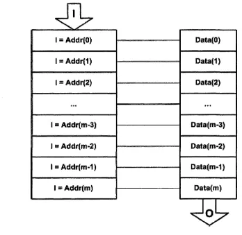
matching. In a standard LUT architecture, shown in Fig. 2.1, an address decoder is
used to m atch the address to a unique stored value.
I - Addr(1}
Figure 2.1: Standard LUT Structure
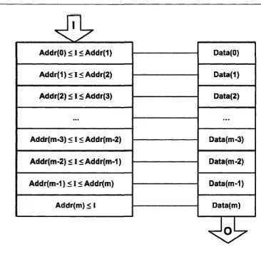
The RALUT architecture of Fig. 2.2, shows the new address decoder system th at
matches a stored value to a range of addresses.
The decoder compares the input address,
I,
to a range of two neighboring mono
tone addresses (e.g., A d d r ( l ) and A d d r(2 )). Only one of these comparisons will
2. MULTI-DIMENSIONAL LOGARITH M IC NUMBER SYSTEM
Addr(1)<l<Addr(2)
Addr(2)i < I < Addr(3)
Addr(rr»»3) < I < Addr(m»2}
Addrfm-1} < I < Addr{m)
Figure 2.2: RALUT Structure
D a ta , to the output, O, of the RALUT. Half of the comparators in the range de
coder can be removed:
(.I < Addr(n
)) = (
Addr(n
) <
I)
(.I > Addr(n))
© ( / >
Addr(n
+ 1)) =
Addr{n)
<
I < Addr(n +
1)
Since the address has a monotone nature, if ( / >
Addr(n
+ 1) ) is true, then (
I
>
Addr(n) )
must also be true. Therefore, the XOR operator can be reduced as:
(J >
Addr(n)).(I > Addr{n
+ 1)) =
Addr{n
) <
I < Addr(n +
1)
2. MULTI-DIMENSIONAL LOGARITH M IC NUMBER SYSTEM
Conversion from a two-digit 2DLNS to binary is a fairly simple process. Both
2DLNS digits are converted separately using the single-digit method, and their re
sults are accumulated to produce the final binary representation. For the reverse
conversion four methods have been developed [16].
1. The
Quick method
chooses the first-digit nearest to the target, and generates the
second-digit to reduce the error, a simple greedy algorithm.
2. The
High/Low method
chooses the two nearest approximations to the target as
the first-digits, generates two associated second-digits for the error, and selects the
combination with the smaller error.
3. The
Brute-Force method
operates by selecting the combination with the smallest
error, but it uses all possible mantissa of
D b
as the first-digits instead of just one
(Quick)
or two
(High/Low).
4. The
Extended-Brute-Force method
improved upon the
Brute-Force method
by us
ing first-digit approximations above 2.0 and below 1.0 (shifted left or right L bits).
Each method ranges from simple implementations and fairly accurate approximations
to difficult implementations and very accurate approximations. All of these methods
have been implemented in fully parametrized Verilog HDL code, which can be found
in [13].
The TLNS (as we name this CPU) CPU design makes use of the two-digit 2DLNS
High/Low
serial converter. Since the filterbank is intended for speech processing and
low power operation, a serial implementation was selected to minimize both power
C hapter 3
T L N S C P U D esign
3.1
O v erv iew o f T L N S C P U D e sig n
The first step in designing a CPU is to determine its applications. The 2DLNS CPU
which we name TLNS hereafter, in addition to performing most traditional arith
metic and logical operations, should also be able to perform some particular tasks.
These special tasks include 2DLNS / Binary conversions, 2DLNS multiplication and
multiply and accumulation, as well as some other operations. Therefore this CPU
is not an application specific design, and can be considered a relatively simple Re
duced Instruction Set Computer (RISC) architecture. The original RISC design of
Hennessy and Patterson
[9] is considered as a conceptual basis in architecture design
of this CPU. The Instruction Set Architecture (ISA) and CPU basic architecture are
modified in order to achieve compatibility with design requirements [1]. We start
by developing the processor’s ISA based on its application. Then the state diagram
3. TLNS CPU DESIGN
conditions th a t cause the CPU to go from one state to another are shown. In the
next step, micro-operations should be developed to fetch, decode, and execute each
instruction. Then we determine the necessary components th a t need to be included
within the CPU. Once this is done, we define the internal d ata paths and necessary
control signals. Finally, we design the control unit, the logic th a t generates the con
trol signals and causes the operations to occur. This is the entire design process to
determine the CPU organization.
3.2
T L N S I n str u c tio n S et A r c h ite c tu r e (IS A )
The Instruction Set Architecture (ISA) is essentially the microprocessor interface. A
microprocessor’s ISA includes information needed to interact with the microproces
sor. The Instruction Set is the set of all assembly language instructions th a t the
microprocessor can execute. In addition, the details of the programmer accessible
registers within the microprocessor are also included in the ISA. These registers store
and perform operations on data. The ISA must specify these registers, their sizes,
and the instructions in the Instruction Set th a t can use each register. The ISA also
includes information necessary to interact with memory [2]. Based on the conducted
research on [15], considering
(B
= 6) for binary base exponent and
(R
= 5) for
second base exponent and an optimal second base of
D =
0.92024380912663017, in
order to convert a 16-bit signed binary d ata to its equivalent 2DLNS representation,
19513 representations of 32768 possible representations, will be error-free (59.5% with
e < 0.5) representations. The remaining 13255 representations have errors from 0.5
to 6. Therefore, in a 1-bit sign 2DLNS representation, considering 24 bits provides a
reasonable mapping precision. In order to keep the TLNS CPU architecture consis
tent, instruction length, register size, d ata buses, and memory words are all designed
3. TLNS CPU DESIGN
as well as processor register set specifications.
3.2.1
R egisters
Registers have a large effect on the performance of a CPU. The CPU can retrieve data
from its register set much more quickly than from memory. Having too few registers
causes a program to refer to memory more often which reduces performance. TLNS
has 16 general-purpose registers, as well as some special-purpose registers. Registers
rO to rl5 are general-purpose registers th a t may be used to hold any 24-bit value,
including d ata and instruction. Register rO is special in th a t it always has the value
0. Any value w ritten into this register is discarded. Register rl4 is used to keep the
equivalent 2DLNS representation for value 1. This value is necessary for using the
MAC unit to perform 2DLNS / Binary conversion. In a 24-bit representation with
two’s-complement representations for both indexes, its Hexadecimal value is 414414.
This value should be preloaded to data memory and w ritten into rl4 by the first in
struction of every program. Register rl5 also has a special application in every “link”
instruction, as we will see later.
The remaining registers have special purposes and are not used to store data.
The program counter (PC) holds the memory address of the next instruction to be
read into the CPU. As mentioned above, each TLNS instruction and memory word
is represented in one 24-bit word. Hence, the PC value is incremented by one after
each instruction is fetched. The memory address register (MAR) is used in order to
specify the next address in d ata memory. There are two other registers named A and
3. TLNS CPU DESIGN
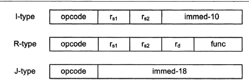
1-type
opcode
rsi
hi
immed-10
R-type
opcode
hi
hi
h
func
J-type
opcode
tmmed-18
Figure 3.1: The three instruction types in TLNS
3.2.2
In stru ction T ypes
As mentioned earlier, each TLNS instruction is encoded in a 24-bit word. There are
three instruction formats, I-type, R-type and J-type, shown in Fig. 3.1. I-type for
m at is generally used for arithm etic and logical instructions th a t have an immediate
operand, and for branch instructions. R-type format is used for arithm etic and logical
instructions th a t operate entirely on register contents. J-type instructions are used
for unconditional jum p instructions, allowing for a larger displacement.
3.2.3
In stru ction Set
The TLNS includes instructions for transferring d ata to and from memory, for per
forming arithm etic and logical operations, for transferring control within a program,
and some special instructions based on 2DLNS. These groups of instructions are de
scribed in the following sections.
It is also helpful to declare a package th a t represents the details of the TLNS
instruction set. This package, which is named tln s_ in s tr, also includes specified en
codings for opcodes. The package first declares bit-vector types for the fields in an
3. TLNS CPU DESIGN
of the instructions in the TLNS instruction set. The opcode
op_special
represents
a class of instructions th a t use R-type format. In this case, the
func
field is used
to specify the instruction. Next, the type
reg_index
represents numeric values for
register numbers. The constants
output_reg_l
and
output_reg_2
specify registers
rl2 and rl3 as output registers for the filter instruction. The rl4 register always
contains the 2DLNS representation of 1. The constant
link_reg
is the number of the
general-purpose register used in “jal” and “jalr” instructions.
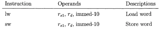
D a ta Transfer Instructions
The TLNS instructions for transferring d ata are listed in Table 3.1, These instruc
tions transfer d ata between the CPU and d ata memory. The memory address for
both load and store instructions is determined by adding the immediate value to the
contents of a base register r 5l, and
is the register whose content is loaded from
memory or stored into memory.
Instruction
Operands
Descriptions
Iw
ra
i,
Td-,
immed-10
Load word
sw
r si,
r^,
immed-10
Store word
Table 3.1: TLNS D ata Transfer Instructions
A rith m etic and Logical Instructions
Table 3.2 shows the TLNS instructions for performing arithm etic operations on bi
nary integer data. Integers are either unsigned or two’s-complement signed values.
3. TLNS CPU DESIGN
rS
2,
with the result overwriting the destination register r^. There are also immediate
forms, in which the second operand is an immediate value. The next two groups
of instructions shown in this table are relational instructions, which compare their
source operands. The conditions th a t can be tested are “eq” (equal to), “ne” (not
equal to), “It” (less than), “le” (less than or equal to), “gt” (greater than) and “ge”
(greater th an or equal to). If the condition is met, the destination register is set to the
integer 1, otherwise it is set to zero [1]. The “lhi” instruction is used to load a 10-bit
immediate value into the most significant 10 bits of the destination register, clearing
the rest 14 bits to zero. The “nop” instruction, as its name suggests, performs no
operation.
The next group of rows in table 3.2 show the logical operations. The “and” , “or”
and “xor” instructions perform the logical operation on corresponding bits from each
of the operands to generate the 24 bits of the result. The immediate versions of these
instructions extend the 10-bit immediate operand to 24 bits by adding zeros to the
left, in order to perform the bitwise logical operation. The first group of shift instruc
tions shift the value read from
rs\
by the number of bits specified in r s2, and store
the results in
The second group shifts the value by the number of bits specified
by the immediate operand.
Control Transfer Instructions
The TLNS instructions to handle transfer of control within a program are listed in
Table 3.3. The branch instruction transfer control to the d ata memory address cal
culated by adding a displacement to the PC. The “beqz” and “bnez” instructions
compare a register
r
si with zero and branch if the condition is met. The next four
3. TLNS CPU DESIGN
Instruction
Operands
Descriptions
add, addu
rs
1,
rB2, rd
Add signed or unsigned
sub, subu
rs
i, r s2,
rd
Subtract signed or unsigned
addi, addui
r sl,
rd,
immed-10
Add signed or unsigned immediate
subi, subui
r s
i,
rd,
immed-10
Subtract signed or unsigned
immediate
sxx, sxxu
rs
i,
r
s2,
rd
Set if condition signed or unsigned
sxxi, sxxui
rs
i,
rd,
immed-10
Set if condition signed or unsigned
immediate
lhi
rd,
immed-10
Load high immediate
nop
No operation
and, or, xor
rs
l,
r
s2,
rd
Bitwise logical and, or, exclusive-or
andi, ori, xori
r si,
rd,
immed-10
Bitwise logical and, or, exclusive-or
immediate
sll, srl, sra
ra
l,
rs2, rd
Shift left-logical, right-logical,
right-arithm etic
slli, srli, srai
rs
i,
rd,
immed-10
Shift left-logical, right-logical,
right-arithm etic immediate
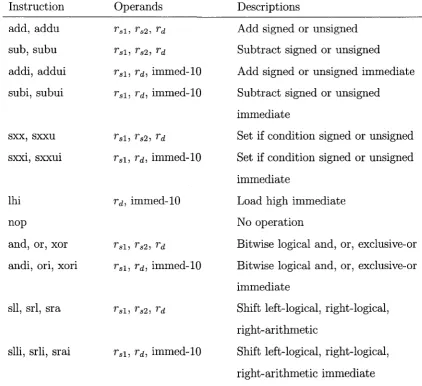
Table 3.2: TLNS Arithmetic and Logical Instructions
displacement to the PC to determine the target address. The “jr” and “jalr” instruc
tions, on the other hand, use the contents of a register
r
si as the target address. The
term “link” in “jal” and “jalr” means th a t these instructions copy the old value of PC
into register rl5 before overwriting it with the target address. The last instruction,
3. TLNS CPU DESIGN
Instruction
Operands
Descriptions
beqz
r sl, immed-10
Branch if register equal to zero
bnez
r si, immed-10
Branch if register not equal to zero
j
immed-18
Jump unconditional
jal
immed-18
Jump and link unconditional
jr
r
si
Jump register
jalr
rsi
Jump and link register
halt
Halt execution
Table 3.3: TLNS Control Transfer Instructions
Special Instru ction s
The final set of instructions provided by the TLNS are special instructions. The first
two instructions are used to provide data transfer between the CPU and the exter
nal world. The “inpt” instruction reads d ata from the external input register to the
destination register r^. The “oupt” instruction writes the contents of the
rs\
register
to the external output register. The “m ult” instruction performs 2DLNS multiplica
tions. The contents of
rsl
and r s2 are operands, and the product is w ritten to r^. A
2DLNS multiply and accumulate is executed by the “filter” instruction. Since this
operation is performed on two sequences of d ata in instruction and d ata memories,
the start addresses of these sequences should be loaded to a register before the “filter”
instruction is executed. This register is addressed by r si. These addresses are incre
mented with each iteration of the instruction execution. While the d ata sequence in
instruction memory is supposed to have a fixed range specified by the least significant
7 bits of the immediate value, the range of the d ata sequence in the data memory
is preloaded to register
r^.
The accumulated results are w ritten to registers rl2 and
3. TLNS CPU DESIGN
Instruction
Operands
Descriptions
inpt
Td
Read input d ata to
rd
oupt
rs
l
Write output d ata from
rsi
mult
r,
,i,
rs2, rd
2DLNS multiplication
filter
rs
i,
r
d, immed-10
FIR filter (Multiply and Accumulate)
tbc
rt
,i,
rd
2DLNS to binary conversion
btc
rsi, rd
Binary to 2DLNS conversion
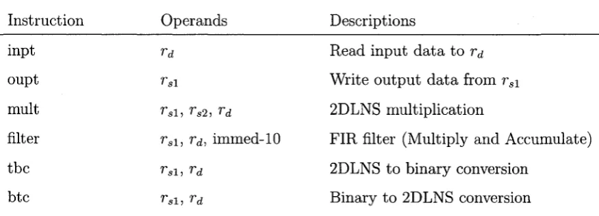
Table 3.4: TLNS Special Instructions
The “tb c” instruction performs 2DLNS to binary conversion. This instruction
converts the contents of r si to 2DLNS representation, and writes the result to
rd.
The “btc” instruction performs the reverse conversion. Again,
rs\
contains the source
2DLNS data, and the converted value is w ritten to
rd.
3.3
T L N S E x te r n a l In terfa ce
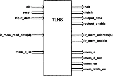
The TLNS CPU makes use of several ports. These are shown in Fig. 3.2. The signal
elk
is the master clock signal th a t drives the CPU. W hen
reset
changes to ‘1’, the
CPU aborts any activity in progress and returns all output signals to their inactive
states. When
reset
returns to
‘0’
, the CPU resumes fetching instructions from in
struction memory address
0.
The CPU uses the
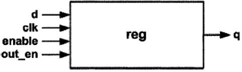
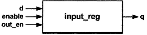
halt
signal to indicate th a t it has
stopped execution. The
ifetch
signal is a status signal th a t the CPU sets to T to
distinguish a read to fetch an instruction from a read to fetch data. The
Input_data
port is used to enter d ata to the CPU, and the
O u tp u t-d a ta
port transfers data
outside of the CPU. The controller sets the
O utput_enable
signal to indicate the
3. TLNS C PU DESIGN
The remaining ports of the CPU are its interface with the instruction and data
memories. The signals
ir_m em _address(a)
and
m em _a
provide the addresses to
access memories. Each address identifies a single word of memory which is equal to
three bytes. The instruction memory words can only be read, and it is done via the
ir_m em_read_data(d)
bus. The controller sets the the
ir_m em _enable
signal to
access instruction memory. D ata memory has separate buses to read d ata from mem
ory,
mem_d_in,
and to write d ata into memory,
mem_d_out.
The
m em _en
signal
is used to enable the CPU to access d ata memory, and the signal
m em _write_en
is
set by the controller whenever d ata memory is accessed to be written.
elk t
reset i
in p u tjfa ta I
ir _ m e r n _ r e a c U d a ta (d ) £
mem d in
TLNS
$h alt
$
(fetch
)
o u tput.data
£ output_enabte
$ ir_m©m_jidd ressfa)
) ir_m#m_enat>ie
J mennja
$ mem_d_out
$ m em .eti
^ mern_write_en
Figure 3.2: The external ports of the TLNS CPU
There are some d ata types used in the TLNS CPU design. These types are all
3. TLNS CPU DESIGN
bit and bit-vector types, and on the numeric bit-vector types defined in the IEEE
nu-m eric_bit
package. The package also defines some other types th a t are used in the
design. The type
tlns_address
represents logic vectors used for address values, and
the type
tlns_w ord
represents logic vectors used for d ata values.
tlns_word_array
represent an array of d ata words. The type
tlns_bus_word
is a standard-logic vector
used for the CPU tristate d ata bus. The constant
disabled_tlns_w ord
is the value
driven by the CPU or memory onto the d ata bus when it is inactive.
3.4
T L N S O p era tio n
In general, a CPU performs three sequences of operation in Fetch, Decode, and Ex
ecute cycles. In the Fetch cycle, the CPU fetches an instruction from memory, then
goes to the Decode cycle. In the Decode cycle, based on the fetched instruction, a
corresponding Execute cycle is determined. Finally, in the Execute cycle, the CPU
executes the instruction and goes to the Fetch cycle to fetch the next instruction.
The controller in the TLNS CPU, is a complex Finite State Machine (FSM) which
realizes CPU operations. The controller is organized as a series of procedures. Each
procedure includes all necessary micro-operations to perform each individual control
task.
Fetching an In stru ction
In the TLNS CPU, an instruction fetch is accomplished by performing two proce
dures. The first procedure,
bus_instruction_fetch_l,
sequences a bus read opera
tion to fetch an instruction from instruction memory. The procedure sets the select
3. TLNS C PU DESIGN
onto the external memory address bus. It sets an instruction fetch (ifetch set to ‘1’)
and sets
ir_m em _enable
to ‘1’ to start the memory operation. The controller then
waits for the successive rising edge of
elk,
and then when the memory operation is
done, executes the
bus_instruction_fetch_2
procedure. This procedure disables the
instruction memory control signal.
D ecod in g th e In stru ction
In order to decode an instruction, two procedures are executed. After an instruction
has been fetched, the
CPU
must increment the program counter. This can be done
by the ALU addition function. The current value of the
PC
is read to
sl_ b u s
and
the controller sends a constant value of 1 to
s2_bus.
These two values are sent to the
ALU, and the result should be w ritten to the
PC
as the next instruction memory ad
dress. This procedure,
instru ction _d ecod e_l,
also considers r sl and
rs2
as registers
which should be read in the first step of each instruction execution, and sets enable
signals for A and B registers, so they are ready to be read. There is an exception for
2DLNS/Binary conversion. In this case, register rl4 is considered as register whose
contents should be read to register B. Again, after one clock cycle, all control signals
are reset through the
instruction_decode_2
procedure. Then, based on the decoded
instruction, the execution state is specified.
E xecu tin g th e In stru ction
The most significant part of the controller, is the part th a t actually executes instruc
tions. Execution starts immediately after the instruction is decoded. The controller
uses a case statem ent to select which group of statem ents to execute, depending on
3. TLNS CPU DESIGN
cedures. Later, when the controller is discussed, these procedures will be described
in detail.
3.5
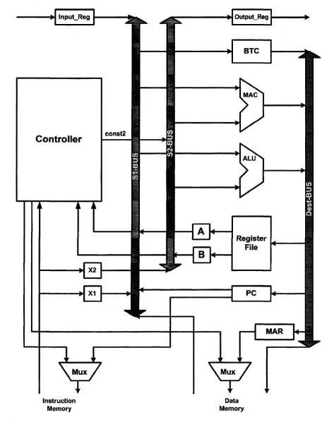
T L N S C P U O rg a n iza tio n
At the Register Transfer Language (RTL) level, the TLNS CPU is composed of reg
isters, buses, multiplexers, an Arithmetic and Logical Unit (ALU), a Multiply and
Accumulate (MAC) unit, a Binary / 2DLNS Converter (BTC), and a sequential con
trol unit. Fig. 3.3 shows the RTL level organization of the CPU upon which we base
our VHDL model.
It includes a register file for the 16 general purpose registers. D ata is written
directly to any of these registers, however the A and B registers are used to store
values read from the register file. The input and output registers transfer d ata to and
from the CPU. The Program Counter (PC) and Memory Address Register (MAR)
are individual registers which are used to address memories. The two multiplexers
allow memory addresses to be determined by the controller as well. The two modules
X I and X2 are extension modules which extend 10-bit or 18-bit immediate values
of instructions to 24 bits for processing by ALU, BTC, or MAC. X2 is also used to
directly pass the 24-bit d ata from instruction memory to
S2_bus.
All ALU and MAC
operations are accomplished in one clock cycle, but the BTC operation needs a vari
able number of clock cycles to be performed. At the start of the operation cycle, the
source operands are placed on the SI and S2 buses, and the operation commences.
At the end of operation, the result is placed on the destination bus, and is stored in
the destination register.
compo-3. TLNS CPU DESIGN
constz
Controller
Instruction
Memory
Data