Fig. 3: Optical Simulation (3D) for 2 gratings: 2400 lines/mm & 1200 lines/mm
Fig. 4: Microscopic image of the fabricated grating
Fig. 4 shows microscopic image of the grating fabricated at TIFR, Mumbai. The grating has 1200 lines/mm and is 5mm×5mm in size. The substrate used is GaAs. Aluminum lines and gold lines of 150nm thickness are made for gratings of 2400 lines/mm and 1200 lines/mm respectively. The width of the lines is approximately 880nm.
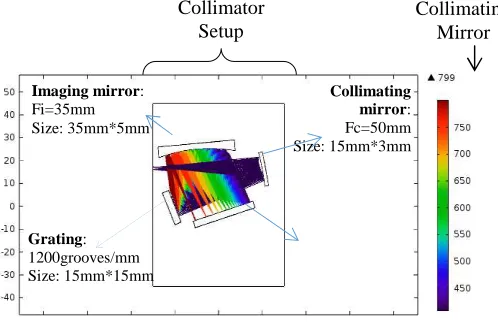
For the optical setup of grating with 1200 lines/mm shown in Fig. 1 the plot of pixel number vs wavelength is shown in Fig. 5. As this plot is non-linear, calibration is done on the P.C. side. The spectrum obtained from the optical setup is acquired and processed by the electronic setup before sending it to the PC.
Fig. 5: Plot of Pixel number vs Wavelength (for 1200 lines/mm)
III. ELECTRONIC DESIGN
Fig. 6: Electronic setup
Fig. 6 shows the block diagram of the electronic setup. The electronic setup has following components:
A. CMOS Sensor
The CMOS sensor S11639 shown in Fig. 7 has 1×2048 pixels and the size of one pixel is 14 µ m×200 µ m [4]. The sensor is driven by 2 clock pulses- ST and CLK. The data output is obtained on the video pin which will be buffered by op-amp LT1818. The buffered signal is given to analog frontend electronics for further signal processing.
CMOS detector
No. of
Imaging mirror
CMOS detector Collimating
mirror
Source
Fig. 7: CMOS sensor
B. Analog Frontend Electronics (AFE)
The AD80066 is a 4-channel analog signal processor. The video signal obtained from the CMOS sensor goes to AFE as one input say on pin VINA [4]. Each channel consists of programmable gain amplifier (PGA), multiplexed to 16-bit ADC. The CDSCLK1 is grounded for SHA mode (sample and hold mode). CDSCLK2 and ADCCLK (CLOCK INPUTS) are given from the microcontroller. The 16-bit digital output is multiplexed into an 8-bit output word available on the 8 data pins D0 to D7, which is accessed using two read cycles. The registers in the AFE are set by using serial interface from the microcontroller.
Fig. 8: AFE IC
C. Line driver
The clocks from the microcontroller are given to the line driver. The line driver improves the rise and fall times of the clock pulses as well as the strength of the signal. Fig. 9 shows the schematic of the line driver IC 74HC541.
Fig. 9: Line Driver
D. Microcontroller
The PIC 18F87J50 microcontroller is used in this design [4]. The clocks driving CMOS Sensor and AFE IC are generated from microcontroller’s CCP/ECCP modules as PWM pulses. The SPI protocol is used to set the registers of AD80066. The data available from AFE is sent to the PC via the microcontroller using USB.
E. Low Noise Voltage Regulator
The CMOS sensor must be protected from any surge voltages which might be caused by peripheral equipment. The CMOS sensor converts charge to voltage at its pixels. Hence the supply of the sensor must be low noise. The low noise regulator LT1965 has low noise of 40µV rms [4].
Fig. 10: Board for PIC18F4550
express our thanks and deep regards for his exemplary guidance, monitoring and constant encouragement in the executed project. We thank our guide Prof. (Dr.) Ketki Kshirsagar for her unrelenting support and guidance through various stages to complete our tasks. I am obliged to thank Prof. Dr. S. S. Prabhu and Mr. Prathamesh Deshmukh at TIFR, Mumbai for all the guidance and help we got. Many thanks to our senior Mr. Ravi Kesharvani for his support and guidance. We also thank Prof. (Dr.) P. D. Khandekar, Head of the Department, Electronics & Telecommunication Engineering, for his appreciation and Prof. Dr. B. S. Karkare, Principal, VIIT, Pune, for her guidance and concern.
REFERENCES
[1] COMSOL Multiphysics, “Czerny-Turner Monochromator” (documentation)
[2] M.V.R.K. Murty, “Theory and Principle of
Monochromators, Spectrometers and Spectrographs”, Optical Engineering (1974)
[3] www.horiba.com
[4] Datasheets of S11639, AD80066, LT1965, PIC18F4550 and PIC 18F87J50