CSEIT1846121 | Published – 08 May 2018 | May-June 2018 [ (4 ) 6 : 643-650 ]
National conference on Engineering Innovations and Solutions (NCEIS – 2018)
International Journal of Scientific Research in Computer Science, Engineering and Information Technology
© 2018 IJSRCSEIT | Volume 4 | Issue 6 | ISSN : 2456-3307
643
Sensor Data Encryption Protocol for Wireless Network Security
(AES Data path Optimization Strategies for Low-Power Low-Energy Multi security-Level Wireless
Network Security Applications)
Dharani. S
Microelectronics and Control System (M.Tech), Electronics and Instrumentation Engineering, Dayananda Sagar College of Engineering, Bangalore, Karnataka, India
ABSTRACT
Network Security is one of the important concept in data security as the data to be made secure. To make data secure, there exist number of algorithm like AES (Advanced Encryption Standard). The security can be enhanced by using standardized and proven-secure block ciphers as advanced encryption standard (AES) for data encryption and authentication. However, these security functions take a large amount of processing power and power/energy consumption. In this paper, we present our hardware optimization strategies for AES for high-speed ultralow-power ultralow-energy IoT applications with multiple levels of security. Our design supports multiple security levels through different key sizes, power and energy optimization for both datapath and key expansion. The estimated power results show that our implementation may achieve an energy per bit comparable with the lightweight standardized algorithm PRESENT of less than 1 pJ/b at 10 MHz at 0.6 V with throughput of 28 Mb/s in ST FDSOI 28-nm technology. In terms of security evaluation, our proposed datapath, 32-b key out of 128 b cannot be revealed by correlation power analysis attack using less than 20 000 traces.
Keywords: Wireless Sensor Network, Wireless Network Security, Network Security,
I.
INTRODUCTION
A wireless Sensor Network is simple defined as a large collection of sensor nodes, equipped with its own sensor, processor and radio transceiver. A wireless sensor network has been widely used in different application areas to know the battlefield situation data, monitoring building parameters and reports about malfunction in a system.
Cryptography, often called encryption, is the practice of creating and using a cryptosystem or cipher to prevent all but the intended recipient from reading or using the information or application encrypted. A cryptosystem is a technique usd to encode a message. The recipient can view the
power. The goal of NIST was to define a replacement for DES that could be used for non-military information security application by US government agencies. Of course, it was recognized that commercial and other non-government users would benefit from the work of NIST and that the work would be generally adopted as a commercial standard. The NIST invited cryptography and data security specialist from around the world to participate in the discussion and selection process. Five encryption algorithms were adopted for study. Through a process of consensus the encryption algorithm proposed by the Belgium cryptographers Joan Daeman and Vincent Rijmen was selected. Prior to selection Daeman and Rijmen used the name Rijndael (derived from their names) for the algorithm. After adoption the encryption algorithm was given the name Advanced Encryption Standard providers of encryption software and hardware have incorporated AES encryption into their products.
The AES encryption algorithm is a block cipher that uses an encryption key and a several rounds of mathematical description of a process of obscuring data. A number of people have created source code implementations of AES encryption, including the original authors.
AES encryption uses a single key as a part of the encryption process. The key can be 128 bits (16 bytes), 192 bits (24 bytes), or 256 bits (32 bytes) in length. The term 128-bit encryption refers to the use of a 128-bit encryption key. With AES both the encryption and the decryption are performed using the same key. This is called a symmetric encryption algorithm. Encryption algorithms that use two different keys, a public and a private key, are called asymmetric encryption algorithms. An encryption key is simply a binary string of data used in the encryption process. Because the same encryption key is used to encrypt and decrypt data, it is important to keep the encryption key a secret and to use keys that are hard to guess. Some keys are generated by software used for this specific task. Another method is to derive a key from a pass phrase. Good encryption systems never use a pass phrase alone as an encryption key.
II.
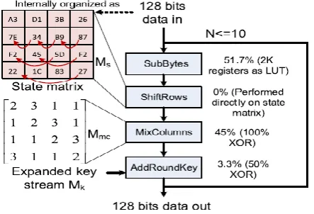
BACKGROUNDA. Preliminary on Advanced Encryption Standard The Advanced Encryption Standard (AES) algorithm operates on plaintext block of 128 bits. The 16-byte input data is internally organized into an array of four rows by four columns, called the state matrix (Ms ). The input data is encrypted by applying a sequence of transformations to the state matrix, as detailed by the pseudo code in Algorithm 1.The flow chart in Figure 1 shows the dominant resources used for the hardware implementation of each transformation module, where the gate utilization data is obtained by synthesizing the AES Verilog code from [20]. The operations performed and the resources consumed for each module are described as follows.
SubBytes module accounts for half of the total gates in AES, with registers used as fixed storage elements of the look-up table (LUT). Each S-box is preconfigured with an 8-bit word in each memory location addressable by an 8-bit input. Hence the LUT size is 28 ・ 8 = 2048 bits. The percentage of hardware resources utilized by this module may vary depending on how the S-box is implemented. If the S-box is implemented by combinational logic circuit, XOR gates become the dominant resources, which account for more than 70% of gate utilization for the AES implementation, as reported in [7].
ShiftRows: The nth row of Ms will be cyclically shifted to the left by n bytes. As shown by arrows on the entries of Ms in Figure 1, the top row is not shifted; the second row is shifted by one byte position; the third row by two; and the fourth row by three. In ASIC design, the ShiftRows transformation can be performed in-place by storing the content of Ms in shift registers, hence no additional logic gate is incurred.
MixColumns: Each column of Ms is multiplied by a constant matrix Mmc consisting of three integer values 1, 2 and 3, as shown in Figure 1. The multiplication of a variable byte by an integer 1, 2 or 3 of Mmc results in an unchanged byte, a 1-bit left shifted byte or the XOR of the byte with a 1-bit left shifted version of itself, respectively. Hence, this invertible linear transformation replaces all four bytes in a column of Ms such that each byte is mixed with all four bytes in the column. This module contains only XOR gates and it accounts for nearly half of the total number of gates.
AddRoundKey: The 16-byte round keys are organized in a similar 4×4 array Mk as the state matrix. Each entry of Mk is denoted as Ki, j . In this operation, each byte Si, j of Ms will be replaced by the result of a bitwise-XOR
operation with a byte Ki, j in the same row and column of the round key matrix Mk . Therefore, the AddRoundKey module is again built by merely XOR gates, which accounts for 3.3% of the total gates.
Figure 1. Flow chart of AES algorithm with gate utilization analysis.
In conclusion, the basic operations involved in AES are XOR, shift, and table look up although the percentage utilization of the logic gates used for each module may vary from design to design.
B. Non-Volatile Logic-in-Memory Architecture Conventionally, all the data is kept in the memory separated from the processor but connected with the I/Os. During the execution, all data needs to be migrated to the processor and written back thereafter. This will cause I/O congestion and impact the system performance for data-intensive application. In addition, significant standby power will be consumed in holding the large volume of data.
Figure 2. Conventional in-memory computing architecture at memory cell level [8].
frequency. However, this solution is limited by the scalability of CMOS technology and has non-trivial cost penalty. Alternatively, the required data communication traffic between memory and processor can be reduced. Instead of feeding the processor with a large volume of raw data, the data can be preprocessed so that the processor needs to deal only with a smaller amount of intermediate results, thereby reducing the communication traffic. The logic-in-memory architecture merges logic with memory to allow some preprocessing to be done locally. Taking the leakage reduction into consideration, the logic in- memory architectures associated with NVM are presented in [8] and [9]. Figure 2 shows the cell-level circuit for the logic-in-memory architecture of [8]. The logic function realized in this example circuit is an in-memory full-adder with both sum logic and carry logic. Instead of reading out the operands, the sum and carry results can be obtained directly after the read operation, as indicated by the red arrow.
III.
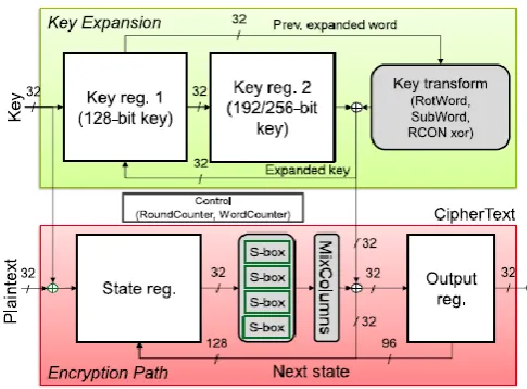
OUR PROPOSED ARCHITECTUREOur proposed architecture is presented in Figure 3. The encryption path includes four parts: a state register; four S-boxes; a MixColumn; and an output register which also acts as a temporary register to store intermediate results. The key expansion consists of two key registers and a key transformation module to support all key sizes specified in AES. Our design is a 32-b datapath architecture, which means the input data and the input key are divided into 32-b chunks. Each pair of 32-b data and 32-b key is loaded together. This takes four cycles to load the 128-b key and 128-b data and XOR them into the state register.
For 192-b keys and 256-b keys, after the first 128 b are loaded, the encryption is started while the other bits of the key are continuously loaded to maximize the throughput. There are two feedback paths, on in the key expansion and the other in the encryption path. The state register needs to be updated every four cycles with new 128-b data, while the
previously expanded word is sent back to the key registers to generate the new expanded key. The details of the optimizations in our proposed architecture are presented in the next sections.
Figure 3. Our proposed AES Architecture
IV.
EXPERIMENTAL RESULTSOur proposed architecture and a lightweight cryptography algorithm PRESENT are modeled in VHDL, synthesized using Synopsys DC Compiler, and fully implemented using Cadence Innovus into the test chip SNACk using ST FDSOI 28-nm technology. The maximum target frequency is set to 60 MHz that provides the maximum throughput of 170 and 106 Mb/s for AES encryption core and PRESENT encryption core, respectively. This throughput meets the demand of mediumand high-throughput IoT applications. AES encryption module and PRESENT encryption module are combined into the block cipher module in SNACk test chip for comparison. The power consumption at different corner cases is estimated using the post signoff extraction. The following sections present our power estimation results on SNACk chip and the security evaluation that we implemented using Synopsys PrimeTime Power.
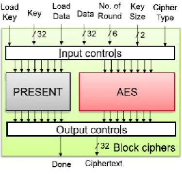
architecture and also a lightweight cryptography algorithm PRESENT for comparison. It has a 32-b data interface with the possibility of selecting different key sizes and the cipher type between AES encryption core and PRESENT encryption core. AES encryption core supports all the encryption modes specified in AES standard including 128-, 192-, and 256-b keys. PRESENT encryption core with the same interface contains two modes: 80- and 128-b keys. The two designs were implemented using the same technology. The test environment for block cipher module in SNACk chip is presented in Figure 9. The plaintext and the key are loaded from the host through SPI interface. Inside SNACk chip, there is an SPI decoder with the APB-like interface to write the test data into the correct memories including the configuration registers, the key memory, the plaintext memory, and the reference memory. After loading all necessary data, the encryption test is done by activating the control finite state machine. If the encryption is done correctly, the running signal will toggle.
Figure 4. Block cipher module in SNACk test chip.
The encryption process continues running repeatedly until the control finite state machine receives the stop signal through the SPI interface. All the power estimation results in the next section are obtained using this test configuration.
Figure 5. Block cipher module in SNACk test chip
B. Power Estimation Results
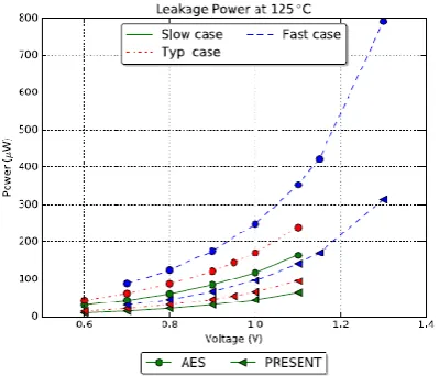
Using the test environment in SNACk chip, it is possible to test two encryption cores with different key lengths at different supply voltages and different operating frequencies. The same key and the plaintexts were sent to each encryption module The activity of the post signoff timing simulation for each encryption module was captured for the whole encryption period. Then, the activity data were used to do power estimation in PrimeTime with FDSOI 28-nm technology libraries provided by ST. The technology librarie were characterized for the supply voltage from 0.6 to 1.3 V for different working conditions. Figs. 10 and 11 show the leakage power and the dynamic power of different encryption modes at 10 MHz withthe supply voltage ranging from 0.6 up to 1.3 V at different corners at 125 °C. It is obvious that the worst case in terms of power consumption is the fast corner. Furthermore, it is clear that there are different leakage powers at different corners, while dynamic powers stay unchanged across different corners. The leakage powers increase significantly when we increase the supply voltage especially in the fast corner. Within the same algorithm, the leakage power has minor differences for different key sizes; however, the leakage power of AES module is fro 2.5 to 3 times the leakage power of PRESENT module.
different key storage, AES module with 128-b key has 20% less dynamic power than AES module with 192- and 256-b keys, while the difference between AES 192- and AES 256-bkeys is a small margin.
The difference among three cornerstested is small. The power consumption decreases gradually when we decrease the supply voltage. The best case in our power estimation results is at 0.6 V where the leakage in different key configuration for the two algorithms is close to each other. At the supply voltage of 0.6 V at typical corner in the worst case of power consumption (at 125 °C), AESmodule consumes the power from 61.5 to 65.6 μW in total an the PRESENT module consumes the power of about 24 μW; while in the typical case at 25 °C, our AES module and our PRESENT module consumes only less than 20 and 12 μW, respectively.
Figure 6. Leakage power at 10 MHz at different supply voltages at different corners.
Figure 7. Dynamic power at 10 MHz at different supply voltages
C. Security Evaluation
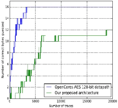
We also perform correlation power analysis (CPA) attack, one of the most effective side channel attacks, on our design using the last round key hypothesis. The attack is based on the power trace extracted through the post signoff power estimation. A simulation of 20 000 encryptions of our design in 128-b key encryption mode is executed to capture th ciphertext and the power traces.
For comparison, we do the same hardware implementation process with a full parallel design from OpenCores. In general, the more parallel level of the datapath, the harder it is to attack the design because parallelism is one way of hiding countermeasures. 8-b datapath without protection is more exposed to this type of attack because the number of traces required to perform the attack is very small. According to DPA contest, even a round-based datapath with full 128-b parallel computation on field-programmable gate array, with good measuremenequipment, only 800 traces are required to reveal the key of the cryptographic devices.
because at the end of each round, the data registers are overridden with new data. This hides the correlation of the activity of the last 4 B of the key which increase the resistance of our design to the last round CPA.
Figure 8. Number of correct guessed key bytes (in 128-b key mode) by last round CPA attack
V.
CONCLUSIONIn this paper, we presented multiple optimization strategies for AES 32-b datapath to achieve a low-cost high-throughput power ultralow-energy design with multiple levels of security.
The area of our proposed architecture is saved by are organization of both datapath and key expansion to minimize the number of registers and control logics. The power consumption is reduced by choosing the S-boxes for low power, by minimizing the activity in the key expansion and in the datapath, and by applying a clock gating strategy to data storage registers. The throughput is maximized by using eight S-boxes and doing key expansion in parallel with the encryption path. Multiple key sizes of the encryption module provide different security levels which help IoT applications to adapt to a wider range of security protocols and mechanisms.
We also showed that our optimization strategies are not only beneficial for area, throughput, and power/energy consumption but also the security
feature. With the optimization in the encryption datapath, 32 b of the secrete key cannot be revealed through CPA attacks with 20 000 traces using last round hypotheses. In terms of power and energy consumption, at 0.6 V at 25 °C, our design can achieve a power consumption of less than 20 μW for all key configurations with the energy consumption of less than 1 pJ/b with the throughput of 28 Mb/s at 10 MHz. In this condition, our AES implementation has nearly the same energy consumption in comparison with the lightweight cryptography algorithm PRESENT on the same technology node: ST FDSOI 28-nm technology. With high throughput ultralow-power, ultralow-energy consumption, our design is obviously suitable for future ultralow-power IoT applications.
VI.
REFERENCES[1] R. Roman, P. Najera, and J. Lopez, ―Securing the Internet of Things,‖ Computer, vol. 44, no. 9, pp. 51–58, Sep. 2011.
[2] A. Barki, A. Bouabdallah, S. Gharout, and J. Traoré, ―M2M security:Challenges and solutions,‖ IEEE Commun. Surveys Tuts., vol. 18, no. 2pp. 1241–1254, 2nd Quart., 2016. [3] S. L. Keoh, S. Kumar, and H. Tschofenig,
―Securing the Internet of Things: A standardization perspective,‖ IEEE Internet Things J., vol. 1,no. 3, pp. 265–275, Apr. 2014. [4] Advanced Encryption Standard, Gaithersburg,
MD, USA, U.S Nat.Institute of Standards and Technology, 2001. [5] IEEE Standard for Local and Mtropolitan Area Networks—Part 15.4: Low-Rate Wireless Persional Area Networks (LR-WPANS), IEEE Standardization Group, Piscataway, NJ, USA, 2011.
[5] LoraWan Specification, LoRa Alliance, Inc., San Ramon, CA, USA, 2015.
[6] Sigfox. Sigfox Technology Overview— Security, accessed on Nov. 15, 2016. [Online]. Available:
[7] Z-Wave Device Class Specification, Sigma Designs, Milpitas, CA, USA, 2016.
[8] A. Bogdanov et al., ―PRESENT: An ultra-lightweight block cipher,‖ in Cryptographic Hardware and Embedded Systems—CHES 2007 (Lecture Notes in Computer Science), vol. 4727, P. Paillier and I. Verbauwhede, Eds. Berlin, Germany: Springer, 2007, pp. 450–466. [9] P. C. Liu, J. H. Hsiao, H. C. Chang, and C. Y.
Lee, ―A 2.97 Gb/s DPA-resistant AES engine with self-generated random sequence,‖ in Proc. Eur. Solid-State Circuit Conf. (ESSCIRC), Sep. 2011, pp. 71–74.
[10] P. Maene and I. Verbauwhede, ―Single-cycle implementations of block ciphers,‖ in Lightweight Cryptography for Security Privacy (Lecture Notes in Computer Science), vol. 9542, T. Güneysu, G. Leander, and A. Moradi, Eds. Cham, Switzerland: Springer, 2016, pp. 131–147. [Online]. Available: https://link.springer.com/chapter/10.1007/978-3- 319-29078-2_8
[11] S. Mathew et al., ―53 Gbps Native GF(24)2 composite-field AES-encrypt/decrypt accelerator for content-protection in 45 nm high performance microprocessors,‖ IEEE J. Solid-State Circuits, vol. 46, no. 4, pp. 767–776, Apr. 2011.
[12] S. Mathew et al., ―340 mV—1.1 V, 289 Gbps/W, 2090-gate nanoAES hardware accelerator with area-optimized encrypt/decrypt GF(24)2 polynomialsin 22 nm tri-gate CMOS,‖ IEEE J. Solid-State Circuits, vol. 50, no. 4, pp. 1048–1058, Apr. 2015.
[13] W. Zhao, Y. Ha, and M. Alioto, ―AES architectures for minimum-energy operation and silicon demonstration in 65 nm with lowest energy per encryption,‖ in Proc. IEEE Int. Symp. Circuits Syst. (ISCAS), May 2015, pp. 2349–2352.