SAMBERG, JOSHUA PAUL. Multi-Quantum Well Structures to Improve the Performance of Multijunction Solar Cells. (Under the direction of Dr. Nadia El-Masry and Dr. Salah Bedair.)
Current, lattice matched triple junction solar cell efficiency is approximately 44% at a solar concentration of 942×. Higher efficiency for such cells can be realized with the development of a 1eV bandgap material lattice matched to Ge. One of the more promising materials for this application is that of the InGaAs/GaAsP multi-quantum well (MQW) structure. By inserting a stress/strain-balanced InGaAs/GaAsP MQW structure into the i-region of a GaAs p-i-n diode, the absorption edge of the p-i-n diode can be red shifted with respect to that of a standard GaAs p-n diode. Compressive stress in the InGaAs wells are balanced via GaAsP barriers subjected to tensile stress. Individually, the InGaAs and GaAsP layers are grown below their critical layer thickness to prevent the formation of misfit and threading dislocations.
Until recently InGaAs/GaAsP MQWs have been somewhat hindered by their usage of low phosphorus-GaAsP barriers. Presented within is the development of a high-P composition GaAsP and the merits for using such a high composition of phosphorus are discussed. It is believed that these barriers represent the highest phosphorus content to date in such a structure. By using high composition GaAsP the carriers are collected via tunneling (for barriers ≤30Å) as opposed to thermionic emission. Thus, by utilizing thin, high content GaAsP barriers one can increase the percentage of the intrinsic region in a p-i-n structure that is comprised of the InGaAs well in addition to increasing the number of periods that can be grown for a given depletion width. However, standard MQWs of this type inherently possess undesirable compressive strain and quantum size effects (QSE) that cause the optical absorption of the InGaAs wells to blue shift. To circumvent these deleterious QSEs stress balanced, pseudomorphic InGaAs/GaAsP staggered MQWs were developed. Tunneling is still a viable mode for carrier transport in the staggered MQW structures.
n solar cells utilizing the improved MQWs are presented.
by
Joshua Paul Samberg
A dissertation submitted to the Graduate Faculty of North Carolina State University
in partial fulfillment of the requirements for the degree of
Doctor of Philosophy
Materials Science and Engineering
Raleigh, North Carolina 2013
APPROVED BY:
_______________________________ ______________________________
Dr. Nadia El-Masry Dr. Salah Bedair
Committee Chair Co-Chair
________________________________ ________________________________
DEDICATION
BIOGRAPHY
ACKNOWLEDGMENTS
TABLE OF CONTENTS
LIST OF TABLES ... viii
LIST OF FIGURES ... ix
CHAPTER 1: Energy ... 1
1.1 Introduction ... 1
1.2 Future Energy ... 1
1.2.1 Biofuel... 3
1.2.2 Biomass ... 3
1.2.3 Geothermal ... 3
1.2.4 Hydroelectricity ... 4
1.2.5 Solar Photovoltaic ... 4
1.2.6 Solar Thermal ... 5
1.2.7 Tidal Power ... 5
1.2.8 Wave Power ... 6
1.2.9 Wind Power ... 6
1.2.10 Nuclear ... 6
1.3 Energy Conclusion ... 7
CHAPTER 2: Photovoltaic Basics ... 9
2.1 Solar Irradiance ... 9
2.2 Photovoltaic Materials Properties ... 10
2.2.1 Crystal Structure ... 10
2.2.2 Energy Band Formation ... 10
2.2.3 Electrons and Holes ... 11
2.2.4 The Formation of Junctions ... 12
2.3 Device Parameters and Principles ... 12
2.3.1 Photocurrent ... 12
2.3.2 Photovoltage ... 13
2.3.3 Fill Factor ... 14
2.3.4 Efficiency ... 14
CHAPTER 3: Multi-junction Photovoltaics ... 19
3.1 Multi-junction Solar Cell Design ... 19
3.2 Materials Selection ... 19
3.2.1 Materials Selection Based on Lattice Matching ... 19
3.2.2 Materials Selection Based on Bandgap ... 20
3.2.3 Materials Selection Based on Current Matching ... 21
3.3 Multi-junction Solar Cell Efficiency Increase ... 21
3.3.1 Improving MJSC Efficiency through Bandgap Engineering and Better Current Matching ... 21
CHAPTER 4: MOCVD Growth ... 28
4.1 MOCVD Growth ... 28
4.2 Metalorganic Precursors ... 28
4.2.1 Metalorganic Precursors: Vapor Sources ... 28
4.2.2 Metalorganic Precursors: Bubblers ... 29
4.3 Basic Components of MOCVD ... 29
4.3.1 Basic Components of MOCVD: Run/Vent Manifold ... 30
4.3.2 Basic Components of MOCVD: Susceptor and Reactor Chamber ... 30
4.3.3 Basic Components of MOCVD: Vacuum/Exhaust System ... 32
4.3.4 Basic Components of MOCVD: Scrubber ... 32
4.4 Substrates, Substrate Preparation and Substrate Loading ... 33
4.4.1 Substrates ... 33
4.4.2 Substrate Preparation ... 34
4.4.3 Substrate Loading ... 36
4.5 Film Growth ... 36
4.5.1 Film Growth: Bake-Out/Purge ... 37
4.5.2 Film Growth: Nucleation ... 37
4.5.3 Film Growth: Bulk ... 37
4.5.4 Film Growth: Termination ... 40
CHAPTER 5: Materials Characterization ... 57
5.1 Characterization ... 57
5.1.1 Optical Microscopy ... 57
5.1.2 X-Ray Diffraction ... 58
5.1.3 Photoluminescence ... 63
5.1.4 Transmission Electron Microscopy ... 64
5.1.5 Hall Effect ... 67
CHAPTER 6: Growth and Characterization of InxGa1-xAs/GaAs1-yPy Strained Layer Superlattices with high values of y (~80%) and Staggered Multi-Quantum Well Structures for Overcoming Quantum Size Effects ... 81
6.1 Abstract ... 81
6.2 Introduction ... 82
6.3 Experimental ... 84
6.4 Results and Discussion ... 85
6.5 Conclusion ... 88
CHAPTER 7: Interface properties of Ga(As,P)/(In,Ga)As Strained Multiple Quantum Well Structures... 96
7.1 Abstract ... 96
7.2 Introduction ... 96
7.4 Results and Discussion ... 98
CHAPTER 8: Effect of GaAs interfacial layer on the performance of high bandgap
tunnel junctions for multijunction solar cells ... 106
8.1 Abstract ... 106
8.2 Introduction ... 106
8.3 Experimental ... 108
8.4 Results and Discussion ... 109
8.5 Conclusion ... 110
CHAPTER 9: Conclusion... 117
9.1... Conclusion ... 117
LIST OF TABLES
Table 1-1: Energy Sources ... 8
Table 3-1: Selected Semiconductor Parameters ... 23
Table 4-1: Pros and Cons of Various Growth Methods ... 41
Table 4-2: Metal-organic Precursors Utilized ... 42
Table 5-1: Materials Parameters for Binary Compounds of Interest ... 67
Table 5-2: Pressure Values for Specific Situations ... 68
LIST OF FIGURES
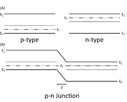
Figure 2-1: AM0 and AM1.5 solar spectrums. ... 15 Figure 2-2: Energy band formation as Si atoms are brought together to form Si bulk solid. 2.35Å is the equilibrium distance for interatomic spacing in Si.25 ... 16 Figure 2-3: Thermal excitation of carriers. The circles represent electrons which can be promoted thermally from the valence band into the conduction band. ... 16 Figure 2-4: Doping of materials to make carrier generation easier. The circles represent electrons which can either be excited from the valence band into an acceptor level or from a donor level into the conduction band. ... 17 Figure 2-5: Carrier excitation through the absorption of a photon. The circles represent electrons which can be promoted due to the absorption of a photon with energy greater than that of the materials bandgap. ... 17 Figure 2-6: (A) A p-type and n-type material separated with their respective Ef labeled and (B) the resultant p-n junction created by bringing the materials together. ... 18 Figure 3-1: Solar spectrum breakdown for the industry standard Ge/(In)GaAs/InGaP MJSC. Higher efficiency is accomplished through better utilization of the spectral regions as
Figure 4-6: Handmade reaction chamber utilized for all growth. ... 48
Figure 4-7: Depiction of the atomic diffusion on the surface of an (A) on axis substrate with no growth steps and (B) off-axis substrate with growth steps. ... 49
Figure 4-8: Calibration curve for InxGa1-xAs as a function of TMIn flux. ... 50
Figure 4-9: Calibration curve for GaAs1-yPy as a function of TBAs flux. ... 51
Figure 4-10: Calibration curve for GaAs:Si carrier concentration as a function of Disilane flux. ... 52
Figure 4-11: Calibration curve for GaAs:Zn carrier concentration as a function of DMZn flux. ... 53
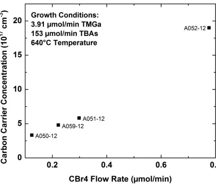
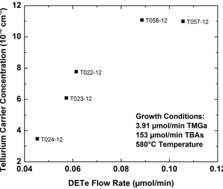
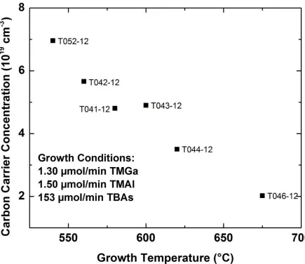
Figure 4-12: Calibration curve for GaAs:C carrier concentration as a function of CBr4 flux. 54 Figure 4-13: Calibration curve for InGaP:Te carrier concentration as a function of DETe flux. ... 55
Figure 4-14: Calibration curve for AlGaAs:C carrier concentration as a function of growth temperature. ... 56
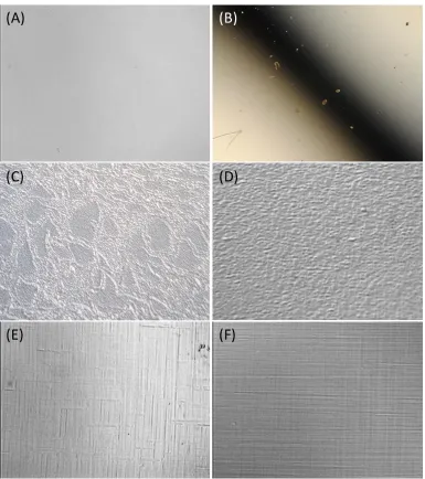
Figure 5-1: Example morphologies for (A) a well prepared and grown featureless sample, (B) a sample with debris most likely due to poor cleaning,21 (C) haziness areas due to poor sample blow-off or exposure to air during solvent/etch procedures and typically occurs near the edge, (D) granular morphology due to a bad growth temperature, (E) misfit dislocations due to tensile relaxation21 and (F) misfit dislocations due to compressive relaxation.21 ... 69
Figure 5-2: XRD calibrations of (A) an InGaAs alloy, (B) a GaAsP alloy and (C) an AlGaAs alloy. Substrate kα1 and thin film kα1 Bragg reflections have been labeled with and S and F, respectively. ... 70
Figure 5-3: Strain effects for (A) tensile strain and (B) compressive strain. Note how the lattice constants for the thin films change. ... 71
Figure 5-4: Young’s Modulus for InGaAs and GaAsP alloys. ... 72
Figure 5-5: Poisson’s ratio for InGaAs and GaAsP alloys. ... 73
Figure 5-6: Relaxed InGaAs and GaAsP alloy lattice constants. ... 74
Figure 5-8: Growth rate of films as a function of indium composition. ... 76 Figure 5-9: XRD (004) 2θ-θ scan of an as-grown MQW structure. ... 77 Figure 5-10: Model of the MQW from Fig. 5-9 in addition to a model of the same structure but with thicker InGaAs and GaAsP layers such that the well/barrier ratio is unchanged. .... 78 Figure 5-11: PL mapping of a MQW structure showing the non-uniformity across the wafer. ... 79 Figure 5-12: Schematic of a TEM specimen stack. ... 80 Figure 6-1: General structure of the MQW demonstrating tunneling through thin (30Å), high composition GaAsP barriers (GaP%>70%). ... 90 Figure 6-2: Staggering of a standard MQW is achieved by moving the portion of on well to an adjacent well. A value of x=50 would result in a staggering ratio (thick well:thin well) of 3:1. ... 90 Figure 6-3: Phosphorus calibration with TBAs flow rate of 20 sccm, TMGa flow rate of 2 sccm and substrate temperature of 600°C. ... 91 Figure 6-4: Zero-Stress balance for GaAs0.2P0.8 barriers. The horizontal line represents the optimum barrier thickness that balances minority carrier transport and QSEs. ... 92 Figure 6-5: (004) XRD data for In0.15Ga0.85As/GaAs0.2P0.8 normal MQW (a), 1.5:1 Stagger MQW (b) and 5.667:1 Stagger MQW (c). ... 93 Figure 6-6: External quantum efficiency for a standard GaAs cell and two staggered p-i-n cells with staggering ratios of 3:1 and 5.667:1. Extension of the band edge is observed the larger a MQW is staggered. (Device fabrication provided by Geoffrey K. Bradshaw) ... 94 Figure 6-7: Staggered band gap model showing how staggering affects the band edge of the MQW. (Modeling provided by C. Zachary Carlin) ... 95 Figure 7-1: (a) The PL data for a series of In0.18Ga0.82As/GaAs0.2P0.8, 20 period MQW
Figure 7-3: HAADF STEM images and EDS plots for two In0.23Ga0.77As/GaAs0.2P0.8, 20 period MQW structures with GaAs transitions of: (a) 70Å at the Ga(As,P) to (In,Ga)As transition but 7Å at the (In,Ga)As to Ga(As,P) transition and (b) 7Å at the Ga(As,P) to (In,Ga)As transition but 70Å at the (In,Ga)As to Ga(As,P) transition. (STEM provided by James M. LeBeau and Hamideh M. Alipour) ... 104 Figure 7-4: EDS line scans of two In0.23Ga0.77As/GaAs0.2P0.8, 20 period MQW structures with GaAs transitions of: (a) 70Å at the Ga(As,P) to (In,Ga)As transition but 7Å at the (In,Ga)As to Ga(As,P) transition and (b) 7Å at the Ga(As,P) to (In,Ga)As transition but 70Å at the (In,Ga)As to Ga(As,P) transition. (STEM provided by James M. LeBeau and Hamideh M. Alipour) ... 104 Figure 7-5: External quantum efficiency for two GaAs-In0.23Ga0.77As/GaAs0.29P0.71 MQW, 10 period devices with MQW GaAs transitions of (a) 15Å at the Ga(As,P) to (In,Ga)As
transition but 7Å at the (In,Ga)As to Ga(As,P) transition and (b) 22Å at the Ga(As,P) to (In,Ga)As transition but 7Å at the (In,Ga)As to Ga(As,P) transition. (Device fabrication provided by Geoffrey K. Bradshaw) ... 105 Figure 8-1: Schematic of the InxGa1-xP:Te/Al0.6Ga0.4As:C tunnel junction. ... 112 Figure 8-2: Typical InxGa1-xP:Te/Al0.6Ga0.4As:C tunnel junction XRD showing the
CHAPTER 1: Energy
1.1 Introduction
Throughout much of history the main energy resources for humans were renewable. Wood was burned to heat homes and cook while the power of water and wind was harnessed to run mills and factories. These renewable energies produce a net zero carbon footprint, the total set of greenhouse gas (GHG) emissions. The technological revolution brought with it the proliferative usage of fossil fuels such as coal, petroleum and natural gas. There is scientific evidence that suggests the burning of these fossil fuels for the last 160 years is contributing to the observed current global climate change.1-2 Carbon dioxide and methane atmospheric, greenhouse gas levels are now at 400 parts per million (PPM)3 and 1800 parts per billion (PPB)4, respectively. While there is some debate as to how much humans have actually contributed to this increase in greenhouse gas levels, whether wholly or in part, there is little debate to what must be done to assuage the contribution by humanity. Transitioning away from fossil fuels to more environmentally responsible renewable energies will greatly reduce the carbon footprint. It is the ultimate goal of the research herein to facilitate a society independent of fossil fuels.
1.2 Future Energy
Coal is the most abundant fossil fuel on the planet and is found mostly in politically stable countries, allowing for reliable reserve values. In most countries coal is used to fire the primary power generation stations. These generation stations provide constant power, also termed basic load, to the grid but not the additional power needed during peak hours. According to the U.S. Energy Information Administration (EIA) in 2010, the estimated recoverable coal reserves are around 948 short tons (1 short ton=2000 lbs.) and would last approximately 222 years.5
Both natural gas and oil are used in powering the secondary power generation stations, the additional power needed during peak demand, and oil is also the primary energy source for transportation. Reserves of natural gas are estimated around 6675 trillion cubic feet by the EIA.6 Natural gas is the fastest growing fossil fuel, primarily due to fracking, and it is expected that a consumption increase of 1.6 percent will occur annually from 2012 to 2035.7 Even with this growth, it is expected that current reserves of natural gas will last 92 years.8 The EIA estimates reserves of oil at 1342 billion barrels. At current consumption levels of 80 million barrels a day this reserve will only last 45 years. Recoverable reserves tend to be a bit pessimistic as they assume no other sources for a given resource will be discovered. Regardless of this fact, fossil fuels are a non-renewable energy which can easily be disrupted by a variety of factors such as natural disaster and political unrest. These factors could lead to volatile pricing for such resources in the very near future.
Ultimately, the most important factor in how much energy will be needed in the future is the population. Population estimates range from 6 to 17 billion9 by the year 2100 with a more conservative estimate by the United Nations of around 11 billion.10 With this increase in population, along with the industrialization of more countries, it is likely the energy demand per capita will continue to increase. However, there are technologies that could help alleviate the increase in energy demand such as LED lighting,11 Energy Star appliances12 and SmartGrid technology.13
which can sustain its consumption rate while renewable energy resources can. Technically, all energy sources listed in Table 1-1 are solar energies with the exception of radioactive fuel. For the intents and purposes of this dissertation, solar energy will only refer to solar photovoltaic energy. The potential sources for energy will be explored in greater depth in the following sections.
1.2.1 Biofuel
Biofuels are derived from biological carbon fixation and include biogases, liquid biofuels and fuels derived from biomass conversions.14 Bioethanol and biodiesel currently constitute the largest segment of biofuel and are used primarily in the transportation sector. In 2010, biofuel production was approximately 700 million barrels and provided 2.7% of the world’s transportation fuel.15
The International Energy Agency (IEA) predicts that biofuels have the potential to supply 27% of the world’s energy fuel demands by 2050.16
1.2.2 Biomass
Similar to biofuel and often used as its presucrsor, biomass is a fuel created by carbon fixation in organisms.17 In its more general form, biomass is plant matter which can be burned to generate electricity. Biomass systems utilize scrubbers similar to that found on fossil fuel systems. These scrubbers clean the air exiting the power plants while the growing crops withdraw CO2 from the atmosphere. Thus, each burning cycle acts like a large cleaning unit for the planet as the crops absorb more CO2 than is released from the power plant. In 2009, the biomass power generating industry in the United States produced 1.4 percent (11,000 MW) of the U.S. electricity supply.18
1.2.3 Geothermal
around 30% of its total electricity in this manner. However, Iceland is ideally situated on the mid Atlantic ridge, making this form of energy production very feasible. Theoretically, the earth’s geothermal resources are enough to supply humanity’s energy needs. However, it is thought that only a small percentage of this resource can be exploited profitably as drilling and exploration for this deep resource is expensive. Nevertheless, over the past 20 years the generating cost of geothermal power has decreased 25%, primarily due to government assistance and subsadies.23
1.2.4 Hydroelectricity
Hydroelectricity is produced by using the gravitational force of falling water. Globally, hydroelectric power generation is by far the most used form of renewable energy. For some countries, such as Paraguay and Norway, nearly 100% of their electric generation is produced in this manner.24 Since 2003, there has been a great increase in the total global electricity production by hydroelectric energy to 3427 TWh in 2010.25 The country with the largest hydroelectric generation capabilities is China at a total 721 TWh in 2010.25 Additionally, China has started or has plans for 15 more large scale hydroelectric power plants adding potentially 60,000 MW of additional electricity.26-27 Hydroelectricity is so widely used because it is cost competitive with fossil fuels. Still, its major detractors relate to the damming of rivers that can harm local ecosystems.
1.2.5 Solar Photovoltaic
the costs in Germany.29 The basics of how solar photovoltaics work will be discussed in more detail in chapter 2.
1.2.6 Solar Thermal
Solar thermal collectors are classified as low, medium or high temperature collectors. While all these will contribute to a cleaner energy future, the following is restricted to the high temperature collectors as they are utilized in electric power generation. High temperature collectors concentrate the solar irradiance using lenses and mirrors. Currently, solar thermal technologies are more efficient than typical photovoltaic technologies30-32 and while only 600MW of solar thermal power was provided worldwide in 2009, current projects will raise this to 14000MW.33 Additionally, solar thermal power is reliable and can deliver peak power loads.34 Unfortunately, solar thermal energy is expensive at around $0.25/kWh with an outlook of $0.12/kWh by the year 2020.35 It does not seem that solar thermal energy will be cost competitive with fossil fuels anytime soon.
1.2.7 Tidal Power
1.2.8 Wave Power
Another type of hydroelectric generation is wave power. Wave power utilizes the energy transported in ocean surface waves to generate electricity. Currently, wave power generation is not a commercially utilized technology as the first experimental wave farm opened in Portugal in 200839 with potential plans for further experimental wave farms.40-42
1.2.9 Wind Power
With the exception of hydroelectric power, wind power is the most utilized renewable energy source. As an alternative energy, wind power is widely distributed, clean and plentiful and uses little land.43 Currently, wind energy comprises 2.5% of the total worldwide electricity usage.44 Additionally, wind power generation is growing around 25% annually. It is exceptionally attractive from a capita standpoint as the cost per unit of energy produced is very similar to that of new coal and natural gas installations.45 Similar to other alternative energies, wind power has its detractors, but while those technologies tend to have detractors of the environmental variety, detractors of wind power are typically concerned with site aesthetics.46 In recent years a new form of wind power has gained attention for the amount of electricity it may be able to produce. This new technology termed high-altitude wind power (HAWP) captures the power of winds high in the sky through a tether and cable.47 The amount of energy that may be produced from HAWP is under debate however, as values ranging from 7.5 TW48 to 1700TW49 have been calculated.
1.2.10 Nuclear
have done little to help assuage the public fear of nuclear energy production.53 Despite these incidences, nuclear power is still the safest form of energy generation in the history of mankind.54-56 Additionally, research continues into making nuclear energy even safer, predominately in the design of reactors.57 Furthermore, the cost of building and maintaining nuclear power plants has become cost prohibitive and many utility companies are choosing not to build plants or are even closing existing plants for these reasons. Nevertheless, nuclear power still has many proponents, such as the World Nuclear Association and the International Atomic Energy Agency (IAEA). Both of which maintain that nuclear power is a viable and sustainable energy source which can be utilized to help reduce carbon emissions.58 Despite public fear, some countries are ramping up nuclear power plant construction, primarily China, which is currently building around 25 nuclear power plants and has plans to build many more.59
1.3 Energy Conclusion
Table 1-1: Energy Sources
Renewable Energies Non-Renewable Energies Biofuel
Fossil: Biomass
Coal Geothermal
Petroleum Hydroelectricity
Natural Gas Solar Photovoltaic Radioactive Fuel:
Solar Thermal
Fission Tidal Power
Cold Fission Wave Power
Fusion
CHAPTER 2: Photovoltaic Basics
Photovoltaics convert sunlight into useable electric energy. The fundamental physics of photovoltaics is well understood with the following references being excellent sources of information.1-5 The following will be the basics of photovoltaics, as the understanding of any technology starts with the basics.
2.1 Solar Irradiance
Photovoltaic energy generation is possible due to the sun’s radiation. A photon of light has a specific energy, , and wavelength, λ, related to each other through:
, [2.1]
where h is Planck’s constant and c is the speed of light in a vacuum. Thus, photons can be characterized by either their energy or wavelength.
2.2 Photovoltaic Materials Properties
The materials properties are of great interest as they can greatly affect the electrical properties of photovoltaics. The basic materials properties pertaining to photovoltaics will be covered in this section. For a more in-depth look as semiconductor materials properties please refer to the following sources.12-15
2.2.1 Crystal Structure
While there are some amorphous and polycrystalline solar cells, the best performance is obtained from single crystal photovoltaics. A crystal structure is that which is composed of a set of atoms arranged in a periodic manner which exhibit order and symmetry over a long range. The structure of a crystal is important as many of its physical properties, such as electrical and optical characteristics, are influenced by the crystal form. Background on crystallography can be found in the literature.16-18
2.2.2 Energy Band Formation
Every object has a wave function, which contains all observable properties of that object. However, the wave function itself cannot be observed. With respect to electrons, when atoms are separated from one another, such that there are no interactions between the two, electrons for the two atoms are allowed to occupy the same quantum states. However, once the atoms begin interacting with one anther the electrons are no longer allowed to have the same quantum states. This applies strictly to fermions and has been termed the Pauli exclusion principle after the Austrian physicist who formulated the principle, Wolfgang Pauli.19 As dictated by the Pauli exclusion principle, when atoms are brought together to form a solid there is a splitting of the discrete energy levels within the atoms. In solids where many atoms are in close proximity to one another continuous bands form as presented in Fig. 2-2.20 The highest occupied molecular band is termed the valence band, while the lowest unoccupied molecular band is termed the conduction band. The separation between these two bands is the bandgap of the material.
with valence bands; essentially, giving the lattice of these materials a sea of electrons which can move and are not locked to atoms. Insulators have a very large separation between valence and conduction bands, while semiconductors have an intermediate separation between the two bands. A more detailed and rigorous investigation to the solution of the actual band structure involves solving the Schrodinger equation,21 typically through the utilization of the Bloch theorem.22-24 This is beyond the scope of a basic understanding of solar cell physics and will not be discussed.
2.2.3 Electrons and Holes
For an intrinsic semiconductor at absolute zero, all electrons are bound to atoms in the crystal lattice and are in the valence band. As the crystal lattice begins to heat, lattice vibration imparts kinetic energy to the electrons, allowing some of them to be promoted into the conduction band. These promoted electrons are now capable of electrical conduction. When these electrons are promoted they leave behind voids in the valence band. These voids can be treated as positively charged particles that are also capable of electoral conduction and have been termed holes. This thermal excitation from absolute zero is presented graphically in Fig. 2-3. Holes are utilized in the valence band because they are easier to keep track of as opposed to the large number of electrons. Thus, intrinsic semiconductors have equal numbers of electrons and holes at all times.
Carrier concentration can be increased by using impurity atoms, termed dopants. These dopants have different valence shell configurations than the host lattice elements. Dopants with a larger number of valence electrons will form energy levels just below the conduction band. These dopants are termed donors and create n-type semiconductors. Dopants with a smaller number of valence electrons will form energy levels just above the valence band. These dopants are termed acceptors and create p-type semiconductors. Thus, doped semiconductors, as opposed to intrinsic semiconductors, do not have the same number of holes and electrons. Doping has been graphically represented in Fig. 2-4.
will be absorbed by electrons in the valence band. These electrons will be promoted into the conduction band and result in a hole being created in the valence band. Photons with energy less than the material bandgap will pass through the material. Carrier generation via photon absorption is presented graphically in Fig. 2-5.
2.2.4 The Formation of Junctions
To understand the formation of junctions we must first define a new parameter, the Fermi level. A Fermi level is a hypothetical energy level that has 50% probability of being occupied at thermodynamic equilibrium.14 Carrier collection is accomplished through the creation of p-n junctions. When materials of two different doping types are brought together, their Fermi levels line up such that they are continuous across the junction, as presented in Fig. 2-6. The end result is the creation of a depletion region and electric field across the junction.
With respect to photovoltaics, carriers generated via photon absorption are separated by the electric field, with holes and electrons being swept in opposite directions. This separation of charge results in a photovoltage, VOC, being produced at open circuit conditions and a photocurrent, ISC, produced at short circuit conditions.
2.3 Device Parameters and Principles
The ultimate goal of a photovoltaic cell is to generate electricity and power. In order to accomplish this, the solar cell must produce both a photocurrent and a photovoltage. In this section, device parameters like photocurrent, photovoltage, fill factor and efficiency will be discussed in general.
2.3.1 Photocurrent
assuming it can occur, throughout a material until the photons are depleted. Thus, generating current is also dependent on the optical absorptive properties of materials. For example, gallium arsenide (GaAs) has a much higher absorption coefficient than germanium (Ge). As such, thicker layers of Ge are required to absorb photons.
With respect to photocurrent, there are two parameters that have been defined for solar cells, each playing an important part in ultimately determining the efficiency of any cell. The first of these parameters is the short-circuit current (ISC). The ISC is a measure of the current produced by the cell when the cell is shorted (zero resistance). The second of these parameters is the maximum-power current (IMP). The IMP is more representative of operational performance of a solar cell as it is the current produced under maximum power conditions. Maximum power conditions will be discussed in more detail in the Fill Factor section.
2.3.2 Photovoltage
The voltage of a photovoltaic single junction cell is directly related to the bandgap of the material used. Higher bandgap materials have promoted electrons with greater energy than lower bandgap materials. Thus, as these higher potential energy electrons build up on the terminals of the p-n photovoltaic device they impart a larger potential energy across the device.
2.3.3 Fill Factor
Fill factor (FF) is used to describe the degree to which the maximum power conditions of any operating photovoltaic device match the upper limits determined by ISC and VOC. The equation for FF is:
. [2.2]
FF for the most efficient photovoltaic cells is around 85% at one sun.
2.3.4 Efficiency
Solar cell efficiency is the ratio of maximum power generated by a solar cell to the incident energy from the sun as presented in the following equation:
. [2.3]
Figure 2-2: Energy band formation as Si atoms are brought together to form Si bulk solid. 2.35Å is the equilibrium distance for interatomic spacing in Si.25
Figure 2-4: Doping of materials to make carrier generation easier. The circles represent electrons which can either be excited from the valence band into an acceptor level or from a donor level into the conduction band.
CHAPTER 3: Multi-junction Photovoltaics
Due to their inefficient utilization of the solar spectrum, single junction photovoltaics are limited in their potential efficiencies. One obvious solution to this limitation is to use a series of junctions to absorb different regions of the solar spectrum. Photovoltaic cells utilizing this technology are termed multi-junction solar cells (MJSC). What follows is a general overview of MJSC technology, the considerations that must be made and ways of improving the technology.
3.1 Multi-junction Solar Cell Design
MJSCs efficiently utilize a larger range of photons by using a combination of semiconductor materials with different bandgaps. The prototypical MJSC is the Ge/(In)GaAs/InGaP triple junction (3J), the spectrum breakdown of which is presented in Fig. 3-1. For comparative purposes, the bandedge for the typical Si solar cell is also included in Fig. 3-1. Due to better utilization of the solar spectrum, MJSC do not suffer from heat losses as typical single junction solar cells do. A diagram showing the lattice constant and bandgap for various semiconductor materials is presented in Fig. 3-2.1
3.2 Materials Selection
Building MJSCs is a complicated endeavor that necessitates compromise in selecting materials. There are three main parameters that must be considered. These parameters are lattice constant, bandgap and current matching.
3.2.1 Materials Selection Based on Lattice Matching
However, for binary materials, each of the sub-lattices is comprised of different elements and is termed Zinc-blend. The bonding between elements is still tetrahedral, as in the diamond structure, but the bonds are all shared between the two elements that comprise the binary semiconductor.
In addition to lattice structure compatibility, the lattice constant of the materials is also important. The lattice constant is a measure of the distance between two atoms occupying lattice points on the corners of the unit cell. It is highly desirable to match the lattice constant of the various layers, although not all MJSC architectures follow this. If there is a mismatch between lattice constants among the materials, defects and dislocations will result as the materials relax. The thickness at which this relaxation occurs is termed the critical layer thickness and can be predicted.2 Defects and dislocations act as recombination centers which result in VOC, ISC and FF degradation.
3.2.2 Materials Selection Based on Bandgap
As the photons comprising the solar spectrum have many different energies, it would be possible, in theory, to select a different material to match each region of the solar spectrum. Additionally, the optimum stack of junctions would depend on where the MJSC was to be operated as the spectrum changes depending on location. A theoretical “infinite junction” would have an efficiency of ~87%.3-4
However, due to lattice matching conditions that must be met; it is not feasible to build MJSC in this manner. The idea of dividing the solar spectrum among materials is still utilized, but only as far as lattice matching conditions allow. The general architecture for a MJSC is presented in Fig. 3-3. The subcells within this MJSC are stacked such that the material bandgaps of the semiconductors decrease as you move into the MJSC. The highest energy photons are absorbed in the top subcell, allowing lower energy photons to pass through unaffected.
3.2.3 Materials Selection Based on Current Matching
Due to the subcells within a MJSC being connected in series, the current generated by the MJSC will be limited to that of the smallest subcell current. This is explained in greater detail in Fig. 3-4. As such, it is desirable that the subcells produce equal current. Unfortunately, current MJSC suffer greatly from inadequate current matching among subcells. Work, including this research, is underway to improve current matching in these structures.
3.3 Multi-junction Solar Cell Efficiency Increase
MJSC efficiency can be improved primarily through two ways. First, MJSC efficiency can be increased through the improvement of current matching among the subcells. Second, MJSC efficiency can be improved by utilizing high solar concentration.
3.3.1 Improving MJSC Efficiency through Bandgap Engineering and Better Current Matching
One way in which MJSC efficiency can be improved is through better current matching among the subcells and through the development of a material with a bandgap of approximately 1.0eV. This has been attempted through a number of different approaches including metamorphic (MM)5-9 growth, inverted metamorphic (IMM)10-14 growth, dilute nitride materials15-19 and pseudomorphic multi-quantum wells (MQWs) structures.19-31
3.3.1.1 Efficiency Improvements: Metamorphic Structure
that the majority of the power produced by the cell comes from the top and middle sub cells. It is for this reason that present metamorphic MJ cells do not reach the efficiencies that would be expected by current matching models.5-9
3.3.1.2 Efficiency Improvements: Inverted Metamorphic Structure
Another solution to overcoming the current matching issues in MJSCs is IMM growth. Similar to MM growth, a graded InGaAs buffer layer is utilized to change the lattice constant of subsequent growth. However, in this method the solar cell is grown upside down with the top cell grown lattice matched to the substrate.10-14 This maintains the top cell as defect free, and also limits the defects from the buffer region into the lower cells which are not as easily affected by defects as the top subcell is. Additionally, the substrate is removed which lowers the total weight of inverted metamorphic MJ cells, great for space applications where payload weight is the main cost consideration. However, the removal of the substrate adds additional complexity to the processing and fabrication of the cell, which consequently results in yield losses and increases the cost of the final product.
3.3.1.3 Efficiency Improvements: Dilute Nitride Based Solar Cells
An additional material which may increase current matching in present MJ cells is InGaAsNSb. While this material system originally suffered greatly from poor minority carrier lifetime and diffusion length, it has been improved greatly in recent years.15-19 However, there still remain some major obstacles to this material becoming a viable option for MJSCs. In particular, the growth is accomplished via molecular beam epitaxy (MBE). MBE is a growth system that is not suited well for large scale industrial applications like metal organic chemical vapor deposition (MOCVD). This is a major hindrance to InGaAsNSb as the bulk of commercial MJSCs are produced via MOCVD.
3.3.1.4 Efficiency Improvements: Pseudomorphic GaAs i-layer MQW Structure
structure to the intrinsic layer, i-layer, of the middle GaAs subcell. The research herein details the development and implementation of such a structure.
3.3.2 Efficiency Improvements: Solar Concentration
For III-V MJSC’s, concentrators are of great importance for terrestrial applications. By concentrating the solar radiation, the total power produced per area of active solar cell is increased, helping to justify the typically high costs of III-V solar cells. Additionally, concentration improves the performance and efficiency of MJSCs due to increased VOC. However, the ability for a cell to work under concentration is at present hindered by the instability of the tunnel junction (TJ) utilized to connect the subcells within the MJSC in addition to the sheet resistance and heat generated. TJs will be discussed in more detail in chapter 8. By improving the TJs within MJSC, higher concentrations could be used, further improving the efficiency of III-V MJSC technology.
Table 3-1: Selected Semiconductor Parameters
Semiconductor Bandgap (eV) Lattice Type Lattice Constant (Å)
Si 1.1132 Diamond 5.4332
GaAs 1.4332 Zinc-Blend 5.6532
InAs 0.3632 Zinc-Blend 6.0632
GaP 2.2632 Zinc-Blend 5.4532
AlAs 2.1632 Zinc-Blend 5.6632
Ge 0.6732 Diamond 5.6532
CHAPTER 4: MOCVD Growth
4.1 MOCVD Growth
Metal-organic chemical vapor deposition (MOCVD) is a growth method in which a thin solid film, usually a semiconductor, is deposited on a solid substrate using organometallic compounds as sources. MOCVD is often used interchangeably with metal-organic vapor phase epitaxy (MOVPE) and organo-metallic vapor phase epitaxy (OMVPE). Throughout this dissertation MOCVD will be used exclusively. The electronic and optoelectronic devices produced via MOCVD are used in a myriad of applications including hetero-junction binary transistors (HBTs) for cell phones1-2, LEDs in traffic lights3-4 and solar cells for electrical generation5. Common to every epitaxial growth technique, MOCVD has its strengths and weaknesses. Among its strengths, MOCVD is the most flexible growth technique capable of large scale production. The reactors are relatively simple when compared to other growth methods and high purity growth is easily obtained with reasonable interface quality. However, the sources employed in MOCVD are oftentimes expensive and many are hazardous. Additionally, MOCVD has the most parameters to control for proper thin film deposition. As such, various factors can interfere with the epitaxy process. Additionally, the thermodynamic and kinetic processes of MOCVD are still not yet fully understood. Stringfellow’s text is a great source and offers details on a wide array of topics relevant to MOCVD epitaxy.6 A list of pros and cons for other thin film growth techniques, in addition to MOCVD, is presented in Table 4-1.
4.2 Metalorganic Precursors
In MOCVD, there are several species utilized to complete the growth of any epitaxial film. These include vapor sources which are premixed with either nitrogen or hydrogen and metal-organic precursors. Both of which will be discussed in some detail in this section.
4.2.1 Metalorganic Precursors: Vapor Sources
dilution manifolds. The dilution manifolds allow for a wider range of source fluxes which can be utilized during MOCVD growth.
4.2.2 Metalorganic Precursors: Bubblers
Organometallic precursors are packaged in stainless steel bubblers, a general schematic of which is presented in Fig. 4-1. The bubbler inlet tube extends nearly to the bottom of the source liquid. As the carrier gas is delivered, it is saturated as it moves though the liquid organometallic precursor. The saturated vapor then moves out through the bubbler exit and is either routed to the vent or run lines via the run/vent manifold. The Thomas Swan MOVCD system can accommodate up to seven bubblers and has been modified to handle an 8th.
There are several desirable properties of precursors that should be taken into account when selecting them. Ideally, although not always possible, they should have a low toxicity. Additionally, it is best if the precursors are liquid at the temperature they are to be used. Liquid sources result in more reproducible growth in addition to good long term stability. Metal-organic precursors should have a suitable vapor pressure for the application in which they are being used. Additionally, their pyrolysis temperature should be similar to the growth temperature to ensure proper decomposition of the precursors. Finally, it is best if the precursors result in low carbon contamination in the epitaxial films. This carbon contamination is typically due to the formation of CH3 radicals that are a byproduct of the pyrolysis reaction. A list of the metal-organic precursors utilized in this research is presented in Table 4-2 along with pros and cons. Additionally, vapor pressure charts and equations for the precursors utilized in this research are presented in Fig. 4-2, 4-3 and 4-4 for column III, column V and dopant sources, respectively.
4.3 Basic Components of MOCVD
4.3.1 Basic Components of MOCVD: Run/Vent Manifold
Precursor delivery is regulated by a computer controlled system utilizing a commercially available software package developed by Thomas Swan (now Aixitron). In general, structures grown via MOCVD are composed of multiple materials and the interfaces between these layers should be sharp to obtain optimum performance of the structure. For this reason, a run/vent manifold, schematic presented in Fig. 4-5,7 is used to help maintain a smooth crystal surface when switching precursor sources. The manifold works by having a carrier gas flow through both lines at all times. The run line goes to the reaction chamber while the vent line bypasses the reactor and goes to the exhaust manifold. The precursor is directed into either the run line or vent line by a block of valves. When a new source is required for the epitaxial growth, the source is first turned on to the vent line. This helps to prevent the growth from being affected by pressure changes due to source turn on. Additionally, both the vent and run lines are held at the growth pressure, further ensuring there are no pressure surges in the MOCVD system as growth is occurring. When the source is needed for growth, it is switched from the vent line into the run line. To accommodate the instantaneous pressure change that would occur during this switching, the MOCVD is equipped with makeup lines to keep the pressure in both the vent and, more importantly, the run line from changing. This is especially important when growing the multi-quantum well structure as trimethyl indium (TMIn) and tributyl phosphine (TBP) vent/run switching occurs frequently. The block for run/vent switching is designed for rapid switching with very small dead volume. The MOCVD is equipped with two run/vent manifolds as the column III and column V compounds have to be separated to prevent gas phase reactions.
4.3.2 Basic Components of MOCVD: Susceptor and Reactor Chamber
Through rotation, all areas of the substrate are equally exposed to both III and V column sources, resulting in better uniformity. Additionally, rotation of the susceptor helps to maintain a uniform growth temperature throughout the substrate. New susceptors undergo a bake to prepare them for MOCVD growth. The procedure is as follows:
1. The MOCVD reactor chamber is purged via a 10 cycle pump purge sequence.
2. The susceptor is slowly ramped to a temperature of 350°C over the course of 2400 secs to drive out any water vapor from the graphite and SiC coating.
3. The susceptor is slowly ramped from 350°C to 900°C over the course of 2400 secs to drive deeper water vapor from the susceptor and help relieve any residual stresses from the fabrication process gradually.
4. The susceptor is kept at 900°C for 1200 secs.
5. The susceptor is cooled to 600°C in preparation for a GaAs epitaxial coating.
6. GaAs is deposited on the susceptor for 900 sec utilizing 3.9 µmol/min of TMGa and 76.5 µmol/min of TBAs.
7. At the conclusion of GaAs deposition the susceptor is cooled to 450°C under an overpressure of TBAs to prevent arsenic desorption.
8. The new susceptor bake is concluded with a 10 cycle pump purge sequence.
The reactor utilized in this research is a custom quartz design, a picture of which is presented in Fig. 4-6. The reactor chamber was produced by Prism Research Glass (Raleigh, NC). Because this is a hand built reactor and the growth rate of the thin films is solely dependent on the delivery of the column III species, reactor orientation must always be kept constant for reproducible results.
4.3.3 Basic Components of MOCVD: Vacuum/Exhaust System
The pressure in the Thomas Swan reactor is controlled by a 25 cubic foot per minute (CFM) Alcatel rotary vane pump and a micro-stepping butterfly valve, both of which are located downstream in the exhaust. The pressure is maintained by a feedback loop made up of a Baratron pressure sensor near the reactor exit and a standard pressure controller. To reduce the occurrence of gas phase reactions, the MOCVD growth is accomplished at a pressure of 200 torr. Reducing the pressure increases the mean free path of the molecules in the reaction chamber, resulting in fewer collisions. This in turn results in fewer gas phase reactions taking place and a better epitaxial growth surface morphology.
In addition to regulating the reactor pressure, the vacuum/exhaust system carries reaction byproducts away from the reactor and to the scrubber. After the reaction chamber, many of the byproducts are volatile and toxic. To help further break these byproducts down, they are passed through a pyrolysis furnace (pyrofurnace) that operates at 400°C. The pyrofurnace is a heated section of tubing containing stainless steel beads to provide a larger surface area over which decomposition can take place. The exhaust is then passed through a particle filter. At this point many of the remaining gaseous byproducts are safe and can be released into the surrounding environment. However, any arsenic containing byproducts must be removed from the exhaust via the scrubber.
4.3.4 Basic Components of MOCVD: Scrubber
The scrubber, produced by Novapure (Norwalk, CT), removes any toxic byproducts from the exhaust that have not already reacted to form inert products. The exhaust gas passes through a proprietary chemisorptive resin before returning to a common exhaust line. This chemisorptive resin reacts with the remaining reactive species in the exhaust and sequesters them. The trapped species are then oxidized periodically to render them inert. The oxidation procedure is as follows:
1. Open the compressed air tank connected to the Novapure scrubber.
2. Set the nitrogen purge on and use the two Matheson flow meters within the scrubber cabinet to set the flow.
phosphorus and arsenic since the last oxidation procedure. Two hours will generally suffice if no calculation is performed.
4. Watch to make sure there are no large temperature changes within the scrubber. There are 5 thermocouples connected to an Omega DP80 readout. Each should be checked.
5. Once the oxidation procedure has finished switch the scrubber purge back to off and close the compressed air.
4.4 Substrates, Substrate Preparation and Substrate Loading
Selection of the proper substrate is imperative for proper MOCVD growth. Additionally, due to the setup of the utilized MOCVD reactor, cleavage of the substrates was necessary. Proper sample preparation procedures prior to substrate loading must be followed to ensure the cleavage of the substrates does not detrimentally effect the epitaxial growth.
4.4.1 Substrates
4.4.2 Substrate Preparation
Many MOCVD reactors utilize wafers larger than 3”. However, to cut down on cost, the research presented herein utilized wafers that were cleaved into 14 mm × 14 mm squares. A 2” wafer results in 7 usable 14 mm × 14 mm substrates. Extreme care was taken when handling the substrates, as any surface damage would have severely affected the quality of the epitaxial growth. As such, all substrate manipulation was handled with Teflon coated tweezers. Additionally, before loading any substrate into the reaction chamber, it was first cleaned in a Teflon beaker by the following procedure:
1. Rinse the substrate well with isopropyl alcohol while ensuring the substrate is never exposed to air. The isopropyl alcohol removes any residual particles from the cleaving process. Isopropyl alcohol is used for this process due to the fact that it is a high purity solvent with a surface tension sufficient enough to remove the particles.
2. Rinse the isopropyl alcohol out with hexane while ensuring the substrate is never exposed to air. The hexane removes any oily/hydrophobic materials that may have contaminated the wafer during the cleaving process. The substrate, completely covered with hexane, should be placed in the sonic bath for no less than 2 mins to ensure the best cleaning.
3. Rinse the hexane out with acetone while ensuring the substrate is never exposed to air. While acetone will help to remove any remaining oily/hydrophobic materials remaining on the substrate, it is predominately used as a step between the hexane and methanol rinses as hexane and methanol are completely immiscible in one another. This is not the case for acetone and methanol. This step does not require any ultrasonic action.
4. Rinse the acetone out with methanol while ensuring the substrate is never exposed to air. The methanol acts to dissolve any hydrophilic compounds that may have contaminated the substrate during the cleaving process. The substrate, completely covered with methanol, should be placed in the sonic bath for no less than 2 mins to ensure the best cleaning. 5. Rinse the methanol out of the beaker using reverse osmosis/de-ionized (RO/DI) water for
several minutes. This is no less than a 10 time (10×) rinse process. It is imperative that the substrate is never exposed to air during this process.
At this point the substrate is properly cleaned of any particles, hydrophobic materials and hydrophilic materials that were introduced during the cleaving process. However, a chemical process is now needed to properly prepare the substrate for epitaxial growth. This process, which is always done immediately following solvent cleaning, is as follows:
both metal and non-metal, from the surface of the substrate which were introduced during the polishing process of the wafer. H2SO4 will also work to remove any oxide on the sample
prior to etching.
2. Rinse thoroughly with RO/DI water for several minutes while ensuring the substrate is never exposed to air. This is a 10× rinse process.
3. Etch the substrate for 30sec with a solution of the following: a) 20ml of DI/RO water.
b) 4ml of ammonium hydroxide (NH4OH).
c) 4ml of hydrogen peroxide (H2O2).
4. With this etch the H2O2 is added last to the solution, as this compound degrades when
exposed to light and heat. This etch solution is utilized to remove any surface and subsurface damage on the substrate and yields a very good surface for epitaxial growth. The etching should only be allowed to proceed for 30 sec to ensure a proper surface is obtained without the danger of over etching. Following this etch procedure should result in ~1 µm of substrate material being etched.
5. Rinse thoroughly with RO/DI water for several minutes while ensuring the substrate is never exposed to air. This is a 10× rinse process.
6. Rinse in hydrochloric acid (HCl) to remove any native oxides that were built up from the previous rinse/etch steps. It is imperative that this HCl etch only be allowed to occur for 1 min. It has been found that etching in HCl for longer than 1 min will result in a sample that is hydrophobic.8
7. Rinse thoroughly with RO/DI water for several minutes while ensuring the substrate is never exposed to air. This is a 10× rinse process.
8. Remove the substrate from the beaker with as much water on its surface as possible. Place the substrate on the vacuum chuck and blow off the water quickly using pure, dry nitrogen. The blow off procedure should be done by directing a jet of nitrogen from one edge of the now cleaned substrate to the opposite edge, driving the water off in a sheet like action. 9. Load the now cleaned substrate into the reactor.
4.4.3 Substrate Loading
The reactor is the location of epitaxial growth. It is maintained at precise temperatures and pressures, and is supplied with the metal-organic vapors. Substrates are loaded into the reactor by removing the quartz reaction chamber. The substrate is then placed onto the susceptor. A cleaned quartz chamber is then placed over the substrate and susceptor. During growth, the quartz chamber accumulates a significant amount of deposition, particularly near the RF coils and below the susceptor. The quartz chamber must be cleaned to prevent contamination from one run to the next. The reaction chamber cleaning procedure is as follows:
1. After each run remove the quartz chamber that was utilized and placed it in a bath of aqua regia (a mixture of 75% HCl and 25% HNO3 by volume). The solution of aqua regia will
rapidly etch the deposition within the chamber, resulting in a clean chamber for subsequent growth.
2. When the contamination is done being etched by the aqua regia (the deposits have been dissolved) remove the chamber from the acid solution. Rinse the outside of the chamber to clean off any remaining aqua regia with RO/DI H2O.
3. Clean the left over silicon grease from the base of the chamber and the inlets with hexane. 4. Rinse the inside of the chamber with RO/DI H2O to clean out any remaining aqua regia. Be
sure to fill the inside of the chamber full of water to be sure all the aqua regia is removed. Aqua regia gives off a vapor that will adhere to the quartz unless solvated in H2O.
5. Rinse the inside of the chamber with methanol to displace any residual water. 6. Dry the chamber with nitrogen.
7. Perform a chamber bake utilizing the Hejet heat gun to evaporate any H2O vapor that may
be desorbed on the quartz.
This process is typically done just prior to substrate preparation. The chamber is allowed to bake with the Hejet while substrate preparation is occurring. After substrate preparation, put new silicon vacuum grease on the inlet tubes and base of the reaction chamber to form vacuum seals with the ultra torr O-rings.
4.5 Film Growth
4.5.1 Film Growth: Bake-Out/Purge
At this point the substrate has been solvent cleaned and etched. However, a thin oxide may have formed on the surface in the process of loading it into the reaction chamber. Additionally, water vapor may be adhered to any surface within the reaction chamber. To purge the reaction chamber of these oxides, H2O vapor and oxygen a bake-out and purge procedure is utilized. At the onset of growth, a pump-purge procedure is started to purge out any oxygen and replace it with nitrogen. This pump-purge procedure is 20 cycles and greatly reduces the amount of oxygen in the reaction chamber. The pump-purge procedure is followed by a 15 minute steady purge which is utilized to further purge the reactor lines. Following the steady purge, the susceptor is heated to 700°C under an overpressure of TBAs to prevent any arsenic desorption. The temperature is held at 700° for 15 mins to bake off any oxide or residual H2O vapor. At this point the substrate and reaction chamber are ready for deposition.
4.5.2 Film Growth: Nucleation
Nucleation is similar for all growth runs. The temperature of the substrate is ramped down from 700°C to 640°C under an overpressure of TBAs to prevent any arsenic desorption. Once the desired temperature is reached the TMGa is introduced into the reaction chamber. A 750-1000Å thick layer of GaAs is deposited with the appropriate doping conditions. This layer is termed the “buffer” layer.
4.5.3 Film Growth: Bulk
accomplished with a reactor pressure of 200 torr and susceptor rotation of 120 rotations per minute (RPM).
A series of bulk calibrations were grown for the following ternary alloys, the application of each is presented in parenthesis: InGaAs (MQW), GaAsP (MQW), AlGaAs (device window). Calibration curves for InGaAs and GaAsP can be found in Fig. 8 and 4-9, respectively. A more in depth look at GaAsP calibrations and growth is presented in chapter 6. In addition to calibration curve generation for ternary alloys, calibration curves were also generated for the following dopants, the application of each is presented in parenthesis: GaAs:Si (devices), GaAs:Zn (devices), GaAs:C (devices), InGaP:Te (tunnel junction) and AlGaAs:C (tunnel junction). The calibration curves for each are presented in Fig. 4-10, 4-11, 4-12, 4-13 and 4-14, respectively. The flow rates are given in µmol/min, a more all-encompassing unit for flow rate as compared to standard cubic centimeter per min (SCCM). The conversion from SCCM to µmol/min is presented in the following section.
4.5.3.1 Micromolar Flow Rate Determination
Micromolar (µmolar) flow rate has been used almost exclusively in this dissertation as a way to greatly simplify the flow parameters under which the growth was accomplished. In this manner, bubbler temperature, flow rate and dilution can all be accounted for in one term. Thus, it is important to understand how the µmolar flow rates were calculated for both bath-based sources and dilute compressed gas sources contained in aluminum cylinders.
4.5.3.1.1 µmolar Flow Rate Determination: Bubbler Sources
The first step in determining the µmolar flow rate of a bubbler source is to determine its vapor pressure. For this, one must first consider how the pressure of a compound relates to the Gibb’s free energy of the compound:
( ) [4-1]
where is the partial pressure, is the change is Gibb’s free energy, is the Gas constant and is the temperature of the compound. Relating 4-1 to the Entropy and Enthalpy of the compound through:
where is the change in enthalpy and is the change in entropy results in the following relationship:
( ) . [4-3]
Through defining the enthalpy and entropy terms as:
[4-4]
and converting 4-3 into log form, the following equation is obtained:
( ) ⁄ . [4-5]
The values of and used to calculate the vapor pressure of the metalorganic sources are presented on the vapor pressure figures. These values result in vapor pressure with units of torr.
Once the vapor pressure of the compound has been determined, the Ideal Gas Law can be rearranged to give:
[4-6]
where is the vapor pressure fraction of the source to the total pressure of the bubbler, is the flow rate in standard liters per minute (SLM), is the absolute temperature,
is the gas constant and is the µmolar flow rate per minute.
4.5.3.1.1 µmolar Flow Rate Determination: Dilute Compressed Gas Source
The determination of µmolar flow rate from dilute zoo tank sources is fairly straight forward. First, the vapor fraction, , of the source must be determined. This value can be found on the source tank and is typically given in values of parts per million (PPM). However, even for most applications, this dilution is still not enough to obtain the desired levels for MOCVD growth. As such, these sources will also go through dilution manifolds which are comprised of a source mass flow controller and a dilution mass flow controller. Thus, the determination of the fraction of this mixture, , resulting from the dilution manifold must be determined. This is accomplished though the following equation:
where is the flow of the source through the source mass flow controller and is the flow of the dilution gas through the dilution mass flow controller. Occasionally, there may be multiple dilution manifolds on a zoo tank source. When this is the case, equation 4-7 will be used once for each dilution manifold. Once has been determined, µmolar
flow rate can be determined. Prior to injection into either the run or vent line, the diluted mixture will pass through a system mass flow controller. This is the last variable in determining the µmolar flow rate. The µmolar flow rate can be calculated through:
, [4-8]
where is the flow through the final, system mass flow controller in standard liters per minute (SLM), 22.4 is the number of liters one mole of a gas occupies at standard temperature and pressure (STP), and is the µmolar flow rate per minute.
4.5.4 Film Growth: Termination
Table 4-1: Pros and Cons of Various Growth Methods
Growth Technique Weaknesses Strengths
MOCVD Expensive Sources
Many Parameters to Control Hazardous Sources
Very flexible
Best for Industrial Applications High Purity
MBE As/P are Difficult
Expensive
Very Low Throughput
Simple
Very Abrupt Interfaces In-situ Monitoring
LPE Scaling Issues
Uniformity Issues
Simple High Purity
HVPE No Al Compounds
Hazardous Sources Difficult to Control
Table 4-2: Metal-organic Precursors Utilized
Metal-organic Precursor
Chemical Equation Disadvantage Advantage
TMGa, Group III (CH3)3Ga C Contamination Liquid,
Good Vapor Pressure TMIn, Group III (CH3)3In C Contamination
Solid
Good Vapor Pressure Also Exists as a Liquid TMAl, Group III (CH3)3Al C Background
Contamination, O Deep Levels
Liquid
Good Vapor Pressure
TBA, Group V (C4H9)AsH2 Expensive Liquid
Good Vapor Pressure Low C Background Low Pyrolysis Temp.
TBP, Group V (C4H9)PH2 Expensive Liquid
Good Vapor Pressure Low C Background Low Pyrolysis Temp. DMZn, p-dopant (CH3)2Zn Zn Diffusion is High Does not Etch
CBr4, p-dopant CBr4 Ozone Depleting
Etches
C Diffusion is Low
Disilane, n-dopant Si2H6 Flammable Good Doping