ABSTRACT
NEWELL, ANDREW PHIFER. Microstructure Studies of Ti-6Al-4V Near-Net Shape Structural Components as Prepared by the Arcam Electron Beam Melting Process. (Under the direction of J. Michael Rigsbee).
The Arcam electron beam melting (EBM) process is used for rapid prototyping of fully functional metallic parts. Arcam uses electron beam scanning technology similar to a scanning electron microscope to form near-net shape components by selectively melting consecutive finite layers of alloy powder according a 3-D computer-aided design (CAD) file. The Arcam EBM process is being considered as a technology that can produce
out-of-production Ti-6Al-4V alloy components for aging aircraft.
Microstructure Studies of Near-Net Shape Structural Components from Ti-6Al-4V as Prepared by the Arcam Electron Beam Melting Process
by
Andrew Phifer Newell
A thesis submitted to the Graduate Faculty of North Carolina State University
In partial fulfillment of the Requirements for the degree of
Master of Science
Materials Science and Engineering
Raleigh, North Carolina 2009
APPROVED BY:
_______________________________ ______________________________
J. Michael Rigsbee Jerome J. Cuomo
Committee Chair Co-chair
DEDICATION
BIOGRAPHY
ACKNOWLEDGMENTS
I would like to graciously thank Dr. J. M. Rigsbee for his patience and guidance throughout the process of this research and for allowing me to serve in many active roles within the North Carolina State University Department of Materials Science and
Engineering. I would also like to thank Dr. Jerome J. Cuomo and Dr. Roger C. Sanwald of the Institute for Maintenance Science and Technology at NC State and the Golden Leaf Foundation for funding this project. I am grateful to Dr. John M. Mackenzie for sharing his expertise in electron microscopy, digital imaging, and for serving on my committee. I would like to thank Dr. Denis R. Cormier of the Department of Industrial Engineering at NC State University and Brian Boyette of NAVAIR for supplying research materials.
Additionally I would like to thank all of those at North Carolina State University who have assisted me with sample preparation and electron microscope operation, which includes Dr. Tom Rawdanowicz and Maria L. Fiedler of the Department of Materials Science and Engineering, Chuck Mooney, Roberto Garcia, Ka C. “Wingo” Wong, and Dale Batchelor of the Analytical Instrumentation Facility, and Valerie Knowlton of the Center for Electron Microscopy in the Department of Microbiology. Other contributions that I am grateful for have come from Danny Brinkley of Progress Energy, John Mastovich, Roger Russell, and Edna Deas.
I am forever grateful to my mother for inspiring and encouraging me to seek higher education, my brother and my father for instilling a strong work ethic and providing
TABLE OF CONTENTS
LIST OF TABLES... vii
LIST OF FIGURES ... viii
1. STATEMENT OF PROBLEM... 1
2. INTRODUCTION ... 4
2.1. The Arcam Electron Beam Melting (EBM) Process ... 4
2.2. The Arcam EBM Process Apparatus ... 7
2.3. Precursor Material (Pre-Alloyed Powder) ... 9
2.4. Component Fabrication Process ... 12
2.5. Electron Beam-Powder Bed Interaction ... 14
2.6. Physical Metallurgy of Ti-6Al-4V Alloy... 17
2.7. Microstructure of Ti-6Al-4V Arcam-Fabricated Parts ... 18
2.8. Surface Morphology of Beam-Melted Metal... 19
3. EXPERIMENTAL PROCEDURE ... 21
3.1. Sample Geometry and Growth Orientation ... 21
3.2. Sample Preparation for Microstructure Analyses ... 28
3.2.1. Optical Microscopy... 28
3.2.2. Scanning Electron Microscopy ... 28
3.2.3. Transmission Electron Microscopy ... 29
3.2.3.1. Electropolishing ... 29
3.2.3.2. Focused Ion Beam... 31
3.3. Optical Microscopy... 32
3.4 Scanning Electron Microscopy ... 32
3.5. Scanning Transmission Electron Microscopy ... 33
3.6. Transmission Electron Microscopy ... 34
3.7. Energy Dispersive X-Ray Spectroscopy... 35
3.8. Grain Size Determination ... 36
3.9. Volume Fraction Determination ... 36
4. RESULTS AND DISCUSSION ... 38
4.1. Exterior Morphology of Arcam - Produced Components... 39
4.1.1. Arcam S12 XY Component ... 39
4.1.2. Arcam S12 XZ Component ... 41
4.1.3. Arcam A2 Horizontal Cylinder Component ... 44
4.2. Microstructure of a Forged Turbine Blade ... 47
4.2.1. Grain Size and Morphology... 47
4.2.2. Description of α + β phase morphology ... 48
4.2.3. Volume fraction of β phase... 49
4.3. Microstructure of Arcam S12 Components ... 51
4.3.1. Grain Size and Morphology... 51
4.3.2. Description of α + β phase morphology ... 61
4.3.4. Transmission Electron Microscopy of S12 - Produced
Components ... 68
4.3.5. Scanning Transmission Electron Microscopy of S12 – Produced Component... 75
4.4. Microstructure of Arcam A2 - Produced Component... 81
4.4.1. Grain Size and Morphology... 81
4.4.2. Description of α + β phase morphology ... 86
4.4.3. Volume fraction of β phase... 88
4.4.4. Transmission Electron Microscopy of A2 - Produced Component ... 89
4.5. Porosity ... 96
4.5.1. Porosity of Arcam S12 – Produced Components ... 96
4.5.2. Porosity of Arcam A2 – Produced Component ... 107
4.5.3. Porosity and Aggregation in PREP Powder... 114
4.6. Transmission Electron Microscopy Sample Preparation... 117
4.6.1. Electropolishing ... 117
4.6.2. Solution to the Porosity Problem ... 126
4.6.2. Focused Ion Beam... 127
5. CONCLUSIONS... 131
6. FUTURE WORK... 134
6.1. Electron Backscatter Diffraction of Growth Plane Normal ... 134
6.2. Hot Isostatic Press (HIP) Arcam Components... 134
6.3. Temperature Measurement of Build Plane ... 135
6.4. Initial Densification of Powder Bed ... 135
6.5. Resistivity Measurement of Powder Bed... 135
6.6. Investigate Possible Presence of FCC Product at α/β Interfacial Phase... 136
LIST OF TABLES
Table 2.1. Titanium alloy composition details used for electron trajectory
simulation... 15
Table 3.1. Electropolishing conditions for Ti-6Al-4V... 32
Table 4.1. Volume fraction of beta phase for forged turbine blade sample ... 50
Table 4.2. Grain size measurements for Arcam S12 produced components... 60
Table 4.3. Volume fraction of beta phase for Arcam S12 produced components ... 68
Table 4.4. Summary of all grain size measurements for all samples ... 60
Table 4.5. Summary table for volume fraction of beta phase for all samples... 89
LIST OF FIGURES
Figure 2.1. Arcam S12 and A2 EBM units [2]... 7 Figure 2.2. Arcam S12 EBM hardware exterior (left) and schematic of solid object
build chamber [8]... 8 Figure 2.3. SEM secondary electron images of gas atomized 2024 Al powder... 10 Figure 2.4. SEM secondary electron images of Starmet PREP Ti-6Al-4V
powder... 11 Figure 2.5. PREP Powder size distribution used in this study ... 12 Figure 2.6. Schematic of electron beam–sample and powder geometry... 14 Figure 2.7. CASINO electron trajectory model for powder bed on solid
titanium alloy ... 16 Figure 2.8. Portion of titanium–vanadium binary phase diagram at 6 wt.%
aluminum [1]... 17 Figure 2.9. Widmanstätten structure formation [13] ... 19 Figure 2.10. Melt pool profiles for surface morphology as it relates to temperature and surface tension ... 21 Figure 3.1. XY sample grown in the Arcam S12. A) Sample schematic. B) Actual
specimen ... 23 Figure 3.2. XZ sample grown in the Arcam S12. A) Sample schematic. B) Top
view of actual specimen. C) Bottom / side view of actual sample ... 24 Figure 3.3. Horizontal Cylinder (HC) sample grown in the Arcam A2.
A) Sample schematic. B) Actual specimen. C) Sectioned specimen... 26 Figure 3.4. XY, XZ and HC sample geometries. Surface planes investigated in
this study are designated by the shaded area and labeled with
Figure 3.6. Illustration of active regimes associated with electropolishing for
current as a function of voltage... 30
Figure 4.1. SEM image of XY Face exterior surface. Growth direction and incident Arcam electron beam are normal to page ... 41
Figure 4.2. SEM image of XY Side exterior surface ... 42
Figure 4.3. SEM image of XZ Face exterior surface ... 43
Figure 4.4. SEM image of XZ Face exterior surface featured in Figure 4.3... 44
Figure 4.5. Optical micrograph of XZ Face mounted, polished and etched ... 45
Figure 4.6. SEM image of HC Face exterior surface, top dead center... 46
Figure 4.7. SEM image of HC Face exterior on a curved surface ... 47
Figure 4.8. Optical micrograph of a Ti-6Al-4V forged turbine blade... 48
Figure 4.9. SEM micrograph of Ti-6Al-4V forged turbine blade ... 50
Figure 4.10. Low magnification optical image of mounted XY Cross Section samples as used for optical and scanning electron microscopy... 53
Figure 4.11. Low magnification optical images of mounted XZ Side sample as used for optical and scanning electron microscopy ... 54
Figure 4.12. Low magnification optical image of mounted XY Face sample as used for optical microscopy and SEM. Component growth is normal to XY Face orientation... 55
Figure 4.13. Low magnification optical image of mounted XZ Cross Section sample as used for optical microscopy and SEM. Component growth is normal to the Cross Section plane for XZ sample ... 56
Figure 4.14. Optical micrograph of XY Face sample ... 57
Figure 4.15. Optical micrograph of XZ Cross Section... 58
Figure 4.16. Optical micrograph of XZ Face ... 59
Figure 4.18. Optical micrograph of XY Side sample. Arrow identifies prior beta
grain boundary ... 63
Figure 4.19. Optical micrograph of XY Face sample ... 64
Figure 4.20. SEM micrograph image of XY Face ... 65
Figure 4.21. SEM micrograph image of XY Cross Section... 66
Figure 4.22. SEM micrograph image of XZ Side ... 67
Figure 4.23. SEM micrograph image of XZ Cross Section ... 68
Figure 4.24. a) Bright field TEM micrograph of XY Side sample and, b) diffraction pattern. Zone axis = [01-12] ... 70
Figure 4.25. Bright field TEM micrograph of XY side sample ... 71
Figure 4.26. Bright field TEM micrograph of XZ Face sample... 73
Figure 4.27. a) Bright field TEM micrograph of XZ Face sample and, b) diffraction pattern. Zone axis = [01-10] ... 74
Figure 4.28. Bright field TEM image of XZ Face FIB sample ... 75
Figure 4.30. STEM image of XZ face FIB sample at 30 KV. Green arrow identifies EDS dot map region... 76
Figure 4.31. STEM image of XZ Face FIB sample at 30 KV. Area used for EDS dot mapping ... 78
Figure 4.32. EDS vanadium (in green) map image of XZ face FIB sample at 30 KV... 78
Figure 4.33. STEM image of XZ face FIB sample at 30 KV. Area used for EDS line scan ... 79
Figure 4.36. Low magnification optical images of mounted horizontal cylinder (HC) sample as used for optical and scanning electron
microscopy... 82 Figure 4.37. Low magnification optical images of horizontal cylinder (HC) sample
used for optical and scanning electron microscopy. Component growth is normal to the face orientation for HC sample ... 83 Figure 4.38. Optical micrograph of HC Face (normal to growth direction) ... 84 Figure 4.39. Optical micrograph of HC Face (normal to growth direction) ... 85 Figure 4.40. Optical micrograph of HC cross section (parallel to growth
direction) ... 86 Figure 4.41. SEM micrograph of HC Face ... 88 Figure 4.42. SEM micrograph of HC Cross Section... 89 Figure 4.43. Bright field TEM micrograph of HC Face and diffraction pattern.
Zone axis = [5-1-43] ... 91 Figure 4.44. a) Bright field TEM micrograph of HC Face and diffraction pattern.
b) Zone axis = [-12-13] ... 92 Figure 4.45. a) Bright field TEM micrograph of HC Cross Section and diffraction
b) pattern. Zone axis = [10-11] ... 94 Figure 4.46. a) Bright field TEM micrograph of HC Cross Section and diffraction
pattern. b) Zone axis = [01-10] ... 95 Figure 4.47. TEM micrograph of HC Face, alpha/ beta phase interface
region ... 96 Figure 4.48. Optical micrograph of XY Cross Section sample near build
plate... 98 Figure 4.49. Optical micrographs of XY Side sample at the build plate ... 98 Figure 4.50. SEM micrograph image of XY Side plane near the build plate ... 100 Figure 4.51. SEM micrograph image of XY Cross Section illustrating
Figure 4.52. Increased magnification SEM micrograph of XY Cross Section
illustrating component fabrication defect from Figure 4.51 ... 102
Figure 4.53. SEM micrograph images of XY Face illustrating incomplete packing and sintering defect ... 103
Figure 4.54. Increased magnification SEM micrograph of XY Face illustrating component fabrication defect from Figure 4.53. Arrows show alpha grain boundary ... 104
Figure 4.55. SEM micrograph of XY Cross Section... 105
Figure 4.56. SEM micrograph of XZ Side ... 106
Figure 4.57. SEM micrograph of HC Face ... 108
Figure 4.58. SEM micrograph of defects in HC Face plane ... 109
Figure 4.59. SEM micrograph of defect in HC Face plane... 110
Figure 4.60. SEM micrograph of HC Cross Section... 111
Figure 4.61. SEM micrograph of HC Cross Section... 112
Figure 4.62. SEM micrograph of HC Cross Section... 113
Figure 4.63. Semi-hollow Ti-6Al-4V PREP powder particle ... 114
Figure 4.64. Ti-6Al-4V PREP powder showing porous particle ... 115
Figure 4.65. Ti-6Al-4V PREP powder showing agglomerated particles ... 116
Figure 4.66. 3mm disc XY Cross Section Ti-6Al-4V TEM sample in Progress... 118
Figure 4.67. 3mm disc XY Cross Section Ti-6Al-4V TEM sample in progress. (Same sample in Figure 4.66) ... 119
Figure 4.70. Electropolished XY Cross Section Ti-6Al-4V 3mm disc TEM
Sample... 121 Figure 4.71. Electropolished XY Cross Section Ti-6Al-4V 3mm disc TEM
Sample... 122 Figure 4.72. Secondary electron SEM image of perforation edge of an
electropolished XY Cross Section Ti-6Al-4V 3mm disc TEM
sample shown in Figure 4.71 ... 123 Figure 4.73. SEM micrograph of HC face Ti-6Al-4V TEM sample in progress... 124 Figure 4.74. SEM micrograph of the surface of an HC face Ti-6Al-4V TEM
sample exhibiting porosity... 125 Figure 4.75. Low magnification optical image of XZ face FIB sample as affixed to
TEM sample mount... 127 Figure 4.76. Image of XZ Face FIB sample (in progress) ... 128 Figure 4.77. Image of XZ Face FIB sample after final thinning... 129 Figure 4.78. XZ face FIB sample as affixed to TEM sample mount. Bottom image
1. STATEMENT OF PROBLEM
The United States military operates aircraft that were initially placed into service as early as the 1960’s. After an airplane or helicopter achieves or exceeds a predetermined number of service hours the unit undergoes a complete ground-up restoration at rebuild depot stations such as NAVAIR at Cherry Point. Many cast and forged components necessary for the remanufacture and repair of these aging aircraft are no longer available from the original manufacturers because the original tooling used for the manufacture of the components are also no longer available and would be extremely expensive to construct. The extensive costs associated with producing the required tooling for the vast number of different components and the limited quantity demanded of each have lead to the pursuit of other means by which to produce discontinued aircraft components.
Additive manufacturing processes using electron beam melting (EBM) are being studied for the production of replacement aircraft components because functional parts with complex geometries can be manufactured without the need of expensive tooling. ArcamAB® has developed an EBM process which can potentially manufacture, using an additive
manufacturing process, fully functional, flight-worthy components using an additive manufacturing process.
The broad objective of this study is to microstructurally evaluate prototype
samples were delivered from early stages of implementation of Arcam processing at NC State University and are not representative of the current work that is being conducted on Arcam EBM process optimization. The Arcam A2 EBM at NC State University is one of the first A2 models installed in North America and the sample used in this study was one of the first pieces to be produced by it. At the time of the A2 installation, the existing Arcam S12 unit was being dedicated to producing components from other alloys, such as aluminum. Components produced by the Arcam S12 and Arcam A2 machines will be evaluated and compared. Because of the complex combination of processing parameters inherent to the Arcam process (e.g., electron beam diameter, powder density and scan rate; powder particle size, shape, and packing efficiency; and, component geometry and size) it is expected that production of components with predictable, consistent microstructures and physical properties will be challenging. The following are the key questions addressed by this research.
1. Are there any significant differences between the two Ti-6Al-4V components produced by the Arcam S12 EBM machine and the one component produced by the A2 EBM machine regarding microstructure?
2. Are the percentage and distribution of alpha and beta phases comparable between the two Ti-6Al-4V components produced by the Arcam S12 EBM machine, the one component produced by the A2 EBM machine, and that for a forged Ti-6Al-4V alloy component? Are these strongly influenced by some processing
2. INTRODUCTION
2.1 The Arcam Electron Beam Melting (EBM) Process
Rapid prototyping (RP) refers to various techniques that create three-dimensional shapes without dies or tooling. As reviewed by Dinda [1] RP includes processes such as selective laser sintering (SLS), stereolithography, direct laser fabrication (DLF), direct metal deposition (DMD), and electron beam melting (EBM). Theses additive processes transform computer aided design (CAD) files of an object into a solid three-dimensional object, which may be either purely geometrically accurate or fully functional.
In what is referred to by Arcam as Adding Technology and CAD-to-Metal [2], a functional part is built layer-by-layer as layers are sequentially fused and solidified in selected areas. The Arcam EBM process used for rapid component prototyping is
operationally similar to the rastering of an electron beam in a scanning electron microscope. In the Arcam process a rastering high power electron beam forms near-net shape components by selectively melting sequential finite-thickness layers of alloy powder in selected area determined by the CAD file of the component geometry. The Arcam process has been successfully implemented by Adler Ortho [3] group of Italy in the fabrication of an
acetabular cup from Ti-6Al-4V for surgical implants in humans where implants need to be specifically shaped for each patient. The implants have been specifically designed to contain 700 mm pores on the surface to promote grafting of new bony tissue without the use of any fiber-tissue interposition [2].
morphology and columnar grains roughly parallel to the incident beam and component growth direction. The length of the columnar grains varied from 5 to 15 mm. The width of the grains were reported to be in the range of 0.15 to 0.8 mm with an average width of 0.3 mm. Tensile and yield strengths of as-deposited components were 1163 +22 and 1105 +19 MPa respectively where the tensile axis was perpendicular to the deposition direction. Elongation under tension was approximately 4 %.
Using direct laser fabrication with a gas-atomized Ti-48Al-2Mn-2Nb powder, Srivastava, et. al, have observed microstructures that range from coarse dendritic, to fine equiaxed, to fine dendritic with increasing laser power [4]. Fine microstructures are expected due to the high cooling rate in the DLF process. Higher laser power is correlated with coarse dendritic microstructure due to high superheating of a larger melt pool and longer
solidification times. Finer and equiaxed microstructures observed from this study are proposed to be due to poor heat dissipation and low cooling rates at lower laser power.
Electron beam melting has been used for many years for welding, zone refinement, refinement of inclusions, and reclamation of scrap [5]. More recently EBM has been advancing as a viable means of manufacturing specialty parts and complex-shaped objects that have comparable properties to those of cast components. Traditionally, part fabrication using EBM has been restricted to rapid part prototyping and research and development environments. Because of its many advantages, especially cost savings, EBM is gaining acceptance as a standard technique for manufacturing complex-geometry functional
tall, the Arcam EBM units efficiently utilize floor space by residing in a 6 ft. wide by 4 ft. deep footprint.
Earlier studies of Ti-6Al-4V alloy parts produced with the Arcam system suggest that mechanical properties such as 0.2% yield strength (149 ksi), ultimate tensile strength (156 ksi), and percent elongation (10.7 %) exceed those for cast parts [6]. Tensile test bars
produced via Arcam EBM [6] have been shown to have tensile strengths that exceed strength values of forged Ti-6Al-4V (0.2% yield strength 120 ksi [7]). Components produced by the Arcam EBM process must meet the minimum standards in Aerospace Material Specification (AMS) 4999 set forth by The Engineering Society For Advancing Mobility Land Sea Air and Space (SAE International) which states that in the beam velocity direction the tensile strength be 130 ksi, 0.2% yield strength be 116 ksi, and elongation be 4%, which is the claim made by Bass [6]. There have been no transmission electron microscopy data published on Ti-6Al-4V components that have been grown in the Arcam S12 or the Arcam A2 EBM machines.
2.2 The Arcam EBM Process Apparatus
The machines used for this study at North Carolina State University are the Arcam EBM S12 and A2 models as shown in Figure 2.1. These systems consist of an electronics control panel and a processing chamber evacuated with a turbomolecular pump backed by a mechanical roughing pump. The processing chamber operating pressure is approximately 1 x 10⁻⁶ Torr. These systems incorporate an electron beam which is generated and scanned in a manner similar to the electron beam in a scanning electron microscope (SEM). The electron beam position is controlled by scan coils as the focused probe is rastered across the powder bed according to the finite cross-sectional area element of the solid object as specified by the CAD file. After each layer of alloy powder has been melted and fused in the specific areas for that specific layer, the build table is lowered approximately 100 microns. Additional powder is delivered from the powder dispensing hopper and spread/raked over the previously solidified layer.
Figure 2.2. Arcam S12 EBM hardware exterior (left) and schematic of solid object build chamber [8].
The electron source is a tungsten filament thermionic emission electron gun and electromagnetic optics are used to focus the beam. Beam potential, EB, is constant at 60 keV.
Typical beam current, iB, values present during the Arcam EBM process range from 3 to 5
mA for aluminum and up to 30 mA for titanium alloys and large areas to be melted. Beam power PB is rated at 3500W [2]. Note that these currents are many orders of magnitude
higher than those encountered in an ordinary SEM, which are typically on the order of nanoamps. Equation 2.1, the brightness equation, could be used in this instance to describe electron gun performance as it includes current density per solid angle α (in steradians) [9] and d is the beam diameter at the powder bed surface, also referred to as probe size or spot
2 2 2 4 α π β d iB
= (2.1)
During EBM processing the beam travels parallel to the powder bed at a velocity VB and will
be assumed for this study to be normal to the processed surface, which is stationary. Electron beam scan rates range from 0.1 m/s to 1000 m/s and will be used for VB. Scan patterns of the
focused beam can be varied also similar to integration image capture options on many SEMs. Variations on beam control include multiple simultaneous actions such as small circular patterns creating a swirling of the melt pool during total planar scan.
2.3 Precursor Material (Pre-Alloyed Powder)
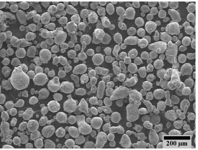
Pre-alloyed powders currently used for EBM are prepared by a gas atomized (GA) process and a plasma rotating electrode process (PREP), a proprietary process for producing ultra-clean spherical powders with smooth surfaces as shown in Figure 2.3. In general, the plasma rotating electrode process takes place as an alloy bar acts as a consumable electrode opposite a plasma in an inert gaseous environment. The alloy bar electrode is rotated about its axis as it is consumed and kept at a constant distance from the plasma. Molten droplets freeze as they are thrown from the bar due to centrifugal force [10]. This process has a high yield at lower energy inputs than the gas-atomized process [11].
method. Figure 2.3 illustrates the surface roughness and irregularity of shape associated with an aluminum alloy powder produced by gas atomization.
Figure 2.3. SEM secondary electron images of gas atomized 2024 Al powder.
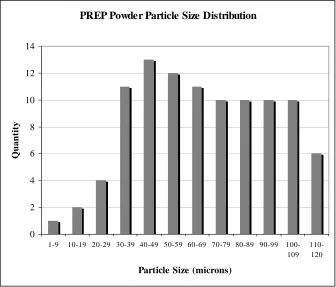
PREP Powder Particle Size Distribution 0 2 4 6 8 10 12 14
1-9 10-19 20-29 30-39 40-49 50-59 60-69 70-79 80-89 90-99 100-109
110-120
Particle Size (microns)
Q u a n ti ty
Figure 2.5. PREP Powder size distribution used in this study.
2.4. Component Fabrication Process
distance between the build plate and the electron beam increases. The heat dissipates to the excess powder surrounding the component being solidified.
The electron beam that performs the melting of the alloy powder is swirled in a triangular pattern 200 to 300 microns in width as it is rastered across the powder bed according to the CAD file cross section.
Figure 2.6. Schematic of electron beam–sample and powder geometry.
2.5. Electron Beam - Powder Bed Interaction
The maximum distance an electron can travel in a given material can be calculated using the Kanaya and Okayama equation (eqn 2.4) for electron range in microns, RKO, which
more specifically is the distance an electron travels until it has zero energy [9. Goldstein]. 0.02760.89 E01.67( m)
Z A
RKO μ
ρ
= (2.4)
A is the atomic weight, Z is the atomic number and E0 is the accelerating voltage in keV,
which is 60 keV in this case. Electron range is inversely proportional to density, ρ, which is known for the alloy of interest to be 4.43 g/cm3.
EB
VB
~100 μm
300 Series Stainless Steel Build Plate
15 mm
T = 600oC
~100 μm d = 100 μm
Ti alloy powder
Table 2.1. Titanium alloy composition details used for electron trajectory simulation.
Alloy Element Ti Al V
wt. % 90 6 4
A (g/mol) 47.9 26.98 50.94
Z 22 13 23
Since we have an alloy, effective atomic weights and numbers must be calculated. Trace elements will be assumed to have negligible effects on electron range and elemental losses experienced during component fabrication.
∑
= = n i i i effecitve AwA
1
(0.90)(47.9) + (0.06)(26.98) + (0.04)(50.94) (g/mol) = 46.77(g/mol)
∑
= = n i i i effecitve Z wZ
1
(0.90)(22) + (0.06)(13) + (0.04)(23) = 21.5
With corrected values, (60 ) ( )
) / 43 . 4 ( ) 5 . 21 ( ) / 77 . 46 ( 0276 .
0 1.67
3 89
.
0 keV m
cm g
mol g
RKO = μ = 17.8μm
To simulate the powder bed as it is used in the Arcam EBM process, the density of a loose powder bed was determined experimentally to be 2.4 g/cm3 by weighing a sampling of the Starmet Ti-6Al-4V powder sample in a small cylinder of volume equal to 8.75 cm3 without packing powder or tapping the side of the cylinder.
that escape the material. Figure 2.7 shows the simulation results using 60keV electrons, a 100 μm stationary probe size, and a 100 μm thick layer of powder on a solid substrate.
Figure 2.7. CASINO electron trajectory model for powder bed on solid titanium alloy.
From the simulation output it is evident that the incident 60 kV electrons do not penetrate past the powder level and into the previous melted layer. This simulation also does not account for the elevated temperature which could further decrease conductivity.
powder
solid
100 μm
2.6. Physical Metallurgy of Ti – 6Al – 4V Alloy
Ti-6Al-4V is a duplex microstructure (alpha and beta) alloy in equilibrium when heated above 980oC and cooled to room temperature. Alpha (α) refers to hexagonal close packed (HCP) crystal structure phase and beta (β) refers to body centered cubic (BCC) crystal structure phase. Figure 2.8 shows an area of the titanium – vanadium binary phase diagram at 6 wt.% aluminum. Elemental titanium is HCP at room temperature but
transforms to BCC above 980 oC, the beta transus temperature. Addition of vanadium (V) stabilizes the BCC β phase to temperatures below 980 oC, with the lowest β to α phase as
shown in Figure 2.8.
Figure 2.8. Portion of titanium–vanadium binary phase diagram at 6 wt.% aluminum [1].
oxidation resistance at high service temperatures [13, 14]. In optical micrographs the alpha phase appears white and beta phase appears black.
A variety of microstructures and properties arise from various heat treatments and mechanical processing. In general there are two types of microstructures. Alpha/beta processed microstructures refer to thermo-mechanically processing the alloy below the beta transus and resulting in equiaxed α grains dispersed in a β matrix. Beta processed
microstructures result in Widmanstätten α lath precipitates distributed in a matrix of β phase from the alloy being thermo-mechanically above the beta transus [24].
Figure 2.9 shows a schematic of Widmanstätten structure formation upon cooling from the beta region into the α + β region of the Ti-V phase diagram at 6%Al.
Figure 2.9. Widmanstätten structure formation [13].
2.7 Microstructure of Arcam - Fabricated Ti-6Al-4V Components
Concurrent studies of Arcam S12-produced components from Ti-6Al-4V have observed columnar grains aligned perpendicular to the growth plane and can extend the length of the sample, which are several millimeters. Columnar grain growth is along the direction of the incident beam direction. Grain structure was equiaxed at the cross sectional area of the columns and roughly 100 to 200 μm in diameter [6]. Microstructure morphology has been noted as fine acicular α (HCP) with β (BCC) phase located between the α phase
Beta transus temp = 980oC
Binary portion of Ti-V phase diagram at 6%Al
Widmanstätten structure development β
grains
α nuclei Τof planes race {110} in β
treatments proved to disrupt columnar grains to some extent while creating coarse α laths and blocky α with discontinuous and coarse α at grain boundaries. The formation of colonies following heat treatments above the β transus were also reported [15].
Murr et al. [16] conducted a study on the microstructure and mechanical properties of Ti-6Al-4V as-deposited using an Arcam S400 EBM. The resultant microstructure was described as Widmänstatten-like, consisting primarily of acicular α-plate.
The claim was also made that as-built components are fully dense and homogeneous, although they state that the alpha plate thickness is wider at the bottom of a 6.8 cm tall vertically grown cylindrical coupon than it is near the top of the coupon [16]. Murr et al. made no mention of columnar grain structure.
2.8. Surface Morphology of Beam-Melted Metal
Figure 2.10. Melt pool profiles for surface morphology as it relates to temperature and surface tension.
Δh
X
Z
h T
γ
3. EXPERIMENTAL PROCEDURE
In the Experimental Procedure chapter the samples used for this study are introduced and categorized by the orientation in which they were grown in the Arcam EBM machines and how samples from the bulk material were prepared for characterization. A total of three samples were available from the Arcam EBM machines; two from the Arcam® S12 and one from the Arcam® A2. Due to the limited number of samples used in this study, the findings reported herein may not be representative of current components being produced by the Arcam S12 and A2 machines at NC State University.
Specific microscopy techniques used are presented including the associated makes and models of equipment employed for this study. The last section of this chapter focuses on sample preparation techniques used for TEM and STEM imaging.
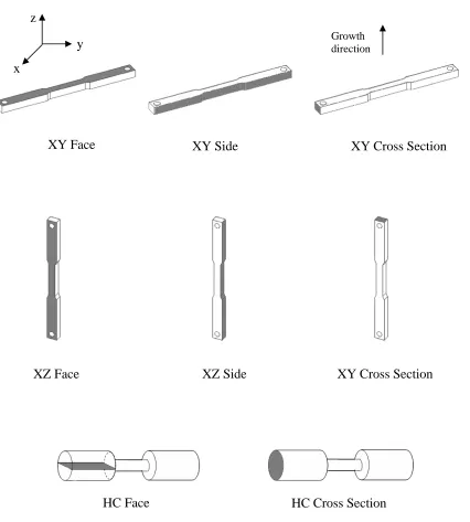
3.1. Sample Geometry and Growth Orientation
“XY” Sample
Figure 3.1. XY sample grown in the Arcam S12. A) Sample schematic. B) Actual specimen.
x y
z A
B
C
“XZ” Sample
Figure 3.2. XZ sample grown in the Arcam S12. A) Sample schematic. B) Top view of actual specimen. C) Bottom / side view of actual sample.
x
y z
Growth direction
A
B
The XY bar original length x width x height dimensions are 121.6 mm x 11.8 mm x 8.03 mm with a center gage section width of 8.55 mm. The XZ bar original dimensions are 121.2 mm x 12.2 mm x 8.22 mm with a center width of 8.70 mm.
The sample produced by the Arcam® A2 machine was a cylindrically-shaped tensile bar grown in horizontal fashion as shown in Figure 3.3. This sample will be referred to as HC to designate a horizontal cylinder. This orientation will be considered equivalent to that of the XY sample.
“HC” Sample
(Horizontal Cylinder)
Figure 3.3. Horizontal Cylinder (HC) sample grown in the Arcam A2. A) Sample schematic. B) Actual specimen. C) Sectioned specimen.
x
y z
Growth direction
B
Figure 3.4. XY, XZ and HC sample geometries. Surface planes investigated in this study are designated by the shaded area and labeled with identification nomenclature.
XY Face x
y z
XY Side XY Cross Section
XZ Face XZ Side XY Cross Section
HC Face HC Cross Section
The as-grown tensile specimens were sectioned for characterization using a Leco V-50 low-speed diamond blade saw and Leco cutting fluid. Samples were cut from the bulk both parallel and perpendicular to the growth direction. The nomenclature adopted for this study consists of face, side and cross section orientations as shown in Figures 3.3 and 3.4.
A Ti-6Al-4V forged helicopter engine turbine blade (Figure 3.5) that was retired from service was also investigated using optical and scanning electron microscopy for comparison of what is considered an ideal representative microstructure for aviation applications. A small section shown in Figure 3.5 was cut by hand using a hacksaw and prepared for optical microscopy and SEM by the same methods described for the Arcam® samples in the
following section.
3.2. Sample Preparation for Microstructure Analyses 3.2.1. Optical Microscopy Sample Preparation
For observation of microstructural features by optical microscopy each orientation sample was mounted in Buehler thermosetting bulk molding compound. Samples were metallographically polished through a series of closed-grit silicon carbide grinding/polishing paper and aluminum oxide water suspension slurry polishing media. The abrasive grit sequence used to polish the optical microscopy and SEM samples was 180, 240, 320, 400, 600, 800, 1000, and 1200 carried out on a South Bay Technologies Model 900 polishing wheel using water as the lubricant. Final polishing was achieved by using 1.0 μm aluminum oxide followed by 0.05 μm aluminum oxide polishing media. Samples were etched in Kroll’s reagent (5% hydrofluoric acid, 10% nitric acid, 85% H2O).
3.2.1. Scanning Electron Microscopy Sample Preparation
The samples that were prepared for optical microscopy were also used for the scanning electron microscopy portion of this study. To eliminate sample charging in the SEM silver paint was applied from the edge of the sample surface to the bottom of the sample where contact was made to the grounded SEM mounting stub.
The PREP powder was prepared for SEM imaging by applying the powder to a stub with carbon tape. Excess powder was removed by gently dusting with dry nitrogen.
3.2.3. Transmission Electron Microscopy Sample Preparation 3.2.3.1. Electropolishing
Electropolishing is a TEM specimen preparation technique that can uniformly remove material from a metal without introducing plastic deformation to the sample. Differential polishing rates (effectively etching) of one phase versus another phase or at grain boundaries is a common but undesirable result of electropolishing multiphase microstructures.
Conductive samples are immersed in an electrolytic solution, which is typically an acid or a mixture of an acid and an organic solvent. The premise of electropolishing lies in achieving equal resistance across the sample surface through the generation and flow of a viscous electrolytic fluid at the sample surface with an applied voltage such that the material is polished rather than etched or pitted [18, 19]. Successful sample preparation requires operation within the polishing regime of the voltage and current curve in Figure 3.6 below.
Figure 3.6. Illustration of active regimes associated with electropolishing for current as a function of voltage.
Pitting
Polishing Current
Etching
Published recommendations for TEM foil preparation of Ti-6Al-4V by
electropolishing were found to be ineffective on the alloy used in this study when followed as prescribed. The parameters described by Kestel [18] which uses 13% HCl and methanol as the electrolytic solution produced undesirable titanium hydride platelets between phases. The parameters described by Blackburn and Williams [20] were successfully used after some modifications in the applied voltage and resultant current.
TEM samples were produced from sections adjacent to those surfaces used for optical and scanning electron microscopy. During the preparation of electron transparent
electropolished samples, care was taken to ensure artifacts were not introduced from the preparation process. Sections ranging from 0.3 to 0.7 mm thick were taken from the bulk material using a slow speed diamond saw. Orientations of interest were either parallel or perpendicular to the growth direction. Three millimeter diameter discs were cut from the sections by either a South Bay Technologies Model 350 abrasive slurry drill or from an Eckert mechanical hole punch device.
The 3mm discs appropriate for TEM samples were mounted with South Bay technologies sample mounting wax to stainless stubs that are used with a Gatan Model 623 Disc Grinder. The samples were mechanically thinned to approximately 25 μm by the same abrasive sequence described for the optical and SEM samples and using a South Bay
Electron transparency of the pre-thinned foils was achieved using a Struers Tenupol-2 electropolishing unit. The electrolytic solution used was 59% methanol, 35% butanol, and 6% perchloric acid. The conditions for successful polishing attempts are listed in Table 3.1 Table 3.1. Electropolishing conditions for Ti-6Al-4V.
Alloy Electroloytic Solution T (oC)
V (volts) I (mA) Jet Speed time (s) Ti-6Al-4V 59% methanol 35% butanol 6% perchloric acid
-50 11 10 - 17 max (10) 30 - 90
3.2.3.2. Focused Ion Beam
Focused ion beam (FIB) technology has greatly expanded the range of materials that can be examined by TEM or STEM because of its ability to produce electron transparent sections from a selected area of virtually any material or part. Similar in construction to an SEM, an electron beam allows the user to image and manipulate a sample while a gallium ion beam mills away material to electron transparency. The sample can then be lifted out of the part and attached to a TEM sample grid.
current. The sample is cut away from the bulk material at 1 nA beam current. Once the FIB sample is attached to the grid on which it will reside, final polishing of the sample is
achieved using the sequence of 1nA, 300pA, and 100pA beam currents.
The FIB has a scanning electron beam in addition to the gallium ion beam. Both ion and electron imaging of a sample in progress is possible. Samples can also be imaged in the FIB by detecting the gallium ions or secondary electrons.
3.3. Optical Microscopy
Imaging of the microstructures in various polished and etched sample orientations were performed on Zeiss MAT 40 Axiovert and Zeiss stereo optical microscopes. Jenoptik ProgRes 10 cameras were used for digital image acquisition.
3.4. Scanning Electron Microscopy
In scanning electron microscopy (SEM) an image is constructed as the signals
voltages in the neighborhood of 20 to 30 keV can be on the order of a few cubic microns, especially for materials of low atomic number and/or low density.
Several scanning electron microscopes were utilized in the characterization of the component exterior morphology, microstructure, and interior fabrication defects. A Hitachi 3200N SEM was used with an accelerating voltage of 20 KV to examine the polished and etched samples of orientations XY side, face and cross-section; XZ side, face, and cross section; and HC face and cross section. The Hitachi 3200N and an Amray 1810 were use at an accelerating voltage of 5 kV for imaging the PREP powder. A JEOL 5900LV operating at 20 KV was used to image the exterior surface morphology of the three types of tensile
specimens. A Hitachi S-5500 ultra-high resolution SEM was used at 30KV to investigate the XZ face TEM sample that was prepared via FIB.
3.5. Transmission Electron Microscopy
Conventional transmission electron microscopy (TEM) produces a direct image of the interior microstructure of a thin sample. In this technique a parallel incident electron beam, typically between 120 keV and 300 keV, interacts with and transmits through the sample forming a 2D projected image of a 3D microstructure onto a fluorescent screen, a charge coupled device (CCD) camera, or directly to exposed film located beneath the sample. TEM is known for extremely high resolution (0.1 nm), however sample preparation is usually quite demanding and time consuming as the sample must be meticulously thinned to achieve electron transparency [21] without introducing artifacts. The types and sizes of TEM
Information available from TEM analyses includes phase morphology, crystal type and orientation, and imaging of defects.
Conventional TEM was carried out for XY side, XY cross-section, XZ face, HC cross section, and HC face on a JEOL 2000FX with a LaB6 electron source operating at 200 KV.
A Gatan CCD camera was used for digital image capture of bright field and diffraction pattern images.
3.6. Scanning Transmission Electron Microscopy
Scanning transmission electron microscopy (STEM) combines elements from conventional TEM and SEM to appropriately handle imaging and microanalysis of thin samples. In this investigation, an SEM with STEM capabilities was used. In STEM the incident beam is focused to a small diameter and rastered across the sample. Differences in intensity are measured point-by-point, but the signals generated by the beam are transmitted through the sample and are collected below the sample.
As the incident beam interacts with a sample, scattering of the incident electrons results in beam broadening. For bulk samples, beam broadening can be in the range of 1000 nm whereas broadening of the electron beam passing through thin film samples is in the 1 to 10 nm range [22]. Resolution in STEM mode is governed by the probe size, which is a function of beam broadening b as defined by the equation:
3/2
2 / 1
0
0 625 107 t
A E
Z b
b ⎟ ×
⎠ ⎞ ⎜ ⎝ ⎛ × × × +
where b0 is the incident focused electron beam probe diameter in nm; Eo is the incident beam
voltage; Z is the atomic number; ρ is the specimen density in g/cm3
; A is the atomic weight, and t is the sample thickness x 10 nm [23]. Image resolution and x-ray microanalysis can be achieved on the nanometer level as the spatial resolution is increased due to the absence of large beam spreading as it passes through a thin specimen.
The Hitachi S-5500 STEM was operated in transmission mode at 30 KV while examining the XZ face of a FIB-prepared sample. A Bruker AXS elemental dispersive x-ray spectroscopy (EDS) system was used on the S-5500 for localized chemical information. EDS data was taken in line and elemental mapping modes.
3.7. Energy Dispersive X-Ray Spectroscopy
Inner shell ionization occurs as the incident electron beam interacts with a tightly bound inner shell electron. The de-excitation that follows an electron transition causes emission of an x-ray that is characteristic of the element under electron bombardment. These characteristic x-rays can be detected and used for qualitative and quantitative elemental analysis.
3.8. Grain Size Determination
Prior beta grain size was approximated per ASTM E 112 by counting the intercepts of a microstructural feature by several lines of known length which were re randomly drawn on optical micrographs. Four random lines of known length were drawn on each of five
different images. The number of intersections between grain boundaries and lines were counted to obtain NL, the number of intercepts per unit length of test line. The grain size G
is determined by using the following relation.
G = -3.2877 + 6.6439 log10NL (Eq. 3.2)
3.9. Volume Fraction Determination
The volume fractions of α and β phases present are estimated using a systematic manual point count per ASTM E 562-08. A regular pattern of intersecting lines is
superimposed over the optical micrographs. The Grid Overlay plug-in in Image J is used to apply an evenly spaced point grid directly to the optical microscope digital images. Points that fall on boundary lines and other questionable intersections are given a value of one half to eliminate bias. The number of points that fall on the minor phase is counted for each image which is defined as Pi. Points that fall on the phase of interest are given a value of
one. PT is the total number of points used on the test grid. Pp is the arithmetic average defined by Eq. 3.3 where n is the number of images used to estimate the volume fraction.
∑
=
= n
i p
p P i
n P 1 ) ( 1
100 ) ( = × T i p P P i
P (Eq. 3.4)
The volume percentage of a phase is thus given by Eq. 3.5.
CI P
VV = p ±95% (Eq. 3.5) 95% CI =is the confidence interval that is given by Eq. 3.6.
⎟⎟ ⎠ ⎞ ⎜⎜ ⎝ ⎛ = n s t CI %
95 (Eq. 3.6)
The variable t is a multiplier that is referenced from Table 1 in ASTM 562-08 and is used to determine the 95% CI and is related to the number of images used for estimating the volume fraction. An estimate of the standard deviation (s) is calculated by Equation 3.7.
[
]
2 12 1 ) ( 1 1 ⎥ ⎥ ⎦ ⎤ ⎢ ⎢ ⎣ ⎡ − − =∑
= n i p p i PP n
s (Eq. 3.7)
The relative accuracy (RA) estimate is obtained by Eq. 3.8. 100 % 95 % = × p P CI
4. RESULTS AND DISCUSSION
This chapter begins with analysis of the exterior surface morphology of as-built Arcam S12 and A2 components using optical and scanning electron microscopy data. Comparisons are made between the forged turbine blade material and the particular three Arcam built samples in the areas of grain size and morphology and, α and β phase
morphology and volume fraction. Quantification of the percentages of the α and β phases were determined from optical and SEM micrographs. In the samples polished and etched with Kroll’s reagent, alpha was white in optical micrographs and black in SEM micrographs. The inverse is true for the beta phase. Grain size of the forged turbine blade and planar cross sections of Arcam components normal to the incident electron (melting) beam was estimated by counting the number of intersections of grain boundaries with a line of known length applied to optical micrographs per ASTM E 112. ASTM E 562-08 is used to describe the estimation of volume fractions of α and β as described in Experimental Procedure, Section 3.8.
The next portion of this chapter focuses on the microstructures of as-built Arcam components are investigated with optical microscopy, SEM and TEM, FIB and STEM were used for sectioning and analyses, respectively, of the XZ Face sample. SEM was used to investigate the intrinsic porosity of the as-built Arcam components.
and the corrective measures for producing successful electron transparent foils from as-built Arcam samples are addressed.
4.1. Exterior Morphology of Arcam Components
The exterior surface morphologies of the near-net shape components produced from the Arcam S12 and A2 EBM machines are presented in this section. Results for the as-built XY and XZ samples precede the horizontal cylinder (HC) sample.
4.1.1. Arcam S12 XY Component
The exterior surfaces of the as-built components produced by the Arcam EBM process shown in this section were cleaned with a wire brush to removed excess PREP powder that surrounded the component in the build tank during component growth but no further sample preparation was performed.
The Arcam electron beam probe diameter was approximately 100 μm and can be as large as 300 μm when the probe is slightly defocused. In Figure 4.1, the Arcam electron beam raster pattern is visible on the top surface of the specimen and the width of the melt pool ranges from 240 to 430 μm which is consistent with the probe size and 200 to 300 micron triangular swirl pattern of the Arcam electron beam.
micrographs of the surfaces of as-built Arcam components, these images show that the Arcam S12 EBM machine produces samples very close to their intended shapes.
Figure 4.1. SEM image of XY Face exterior surface. Growth direction and incident Arcam electron beam are normal to page.
The exterior side surface of the as-built XY sample is shown in the SEM micrograph in Figure 4.2. As expected, surface topography is not as uniform or smooth, as is observed on the XY Face surface topography shown in Figure 4.1. Spherical powder particles from the surrounding area of the build tank are sintered onto the exterior surface of the sides of a component. The bottom of the sample in Figure 4.2 is the part of the component that is in contact with the build plate. Consequently a final finishing, such as sandblasting, machining,
and polishing steps would be required to produce a smooth surface with no unmelted powder particles.
Figure 4.2. SEM image of XY Side exterior surface.
4.1.2. Arcam S12 XZ Component
The XZ Face surface of the tensile bar at the gage length area where its cross section is reduced is featured below in Figure 4.3. Distinct ledges are visible that are the result of additive deposition layers. The tensile bar is imaged on its side and the growth direction of the component is from right to left. The layers visible in this image are the build steps and are spaced approximately 360 to 410 microns apart. Careful examination of the image reveals that the incomplete melting of the powder creates notches between build layers and likely will result in increased porosity in the midline between build layers. Since the sample is
surrounded by the alloy powder as a component is being built, some of the powder particles fuse to the sample from the residual heat available in the component.
Figure 4.3. SEM image of XZ Face exterior surface.
Figure 4.4 is a higher magnification SEM micrograph of the XZ sample in Figure 4.3.
PREP powder spheres attached to the exterior. The sample had been handled and cleaned with a wire brush upon removal of the Arcam S12 EBM machine.
Figure 4.4. SEM image of XZ Face exterior surface featured in Figure 4.3.
and are not in contact with the component. Some of the spheres are clearly partially sintered to the component as seen in Figure 4.5.
Deposition layer heights measured from Figures 4.3 and 4.4 are well above the 100 μm layer height that is controlled by the Arcam EBM machine. This suggests that the
machine does not actually control component growth in 100 μm layers as indicated by the build data that is logged by the software associated with the Arcam EBM machines.
Figure 4.5. Optical micrograph of XZ Face mounted, polished and etched.
4.1.2. Arcam A2 Horizontal Cylinder Component
The exterior surface of the horizontal cylinder (HC) grown in the Arcam A2 EBM machine is shown in the SEM micrographs in Figures 4.6 and 4.7 of the HC Face surface.
the melt pool is approximately 150 μm. The width of the melt pool in this region is 2 mm. The top surface of the sample has some remnants of the PREP powder spheres that are partially sintered to the surface at the melt pool edge.
Figure 4.6. SEM image of HC Face exterior surface, top dead center.
4.2. Microstructure of a Forged Turbine Blade
4.2.1. Grain Size and Morphology
The optical micrograph in Figure 4.8 is a polished and etched forged Ti-6Al-4V helicopter engine turbine blade that has been retired from service and is representative of the bulk material. The grain structure is equiaxed and represents an ideal grain size and shape for a many Ti-6Al-4V aircraft components. The forging process followed by a
recrystallization anneal, typically 4 hours at 925oC [13], provide the thermo-mechanical energy required to obtain the equiaxed microstructure seen in Figure 4.8.
Grain size is estimated by using the ASTM E 112 intercept method described in Section 3.8 of Experimental Procedure. The number of intercepts per unit length of test line is for the forged turbine blade is 172.55 which gives a grain size of G = 12 when applied to Eq. 3.2. This correlates to an average grain size of 6.7 μm.
4.2.2. Description of α + β Phase Morphology
Alpha phase appears light and beta phase appears dark in the optical micrograph in Figure 4.8. The microstructure of this specimen is equiaxed alpha grains in transformed beta matrix (intergranular), which contain coarse acicular α phase. Figure 4.9 is an SEM
Figure 4.9. SEM micrograph of Ti-6Al-4V forged turbine blade.
4.2.3. Volume Fraction of β Phase
Table 4.1. Volume fraction of beta phase for forged turbine blade sample.
Component Type
Volume Fraction of Beta Phase
(%)
Relative Accuracy (%)
4.3. Microstructure of Arcam S12-Produced Components
4.3.1. Grain Size and Morphology
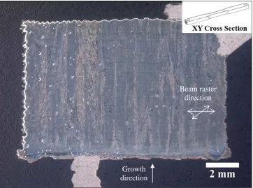
Figure 4.10 shows a cross section of the XY sample that was grown in the Arcam S12 EBM machine. This sample oriented in the XY Cross Section view was mounted in a
thermosetting bulk molding compound and, after grinding and polishing, was etched with Kroll’s reagent. The columnar structure observed here is oriented parallel to the rastered incident electron beam. These grain-like structures extend several millimeters, which in the case of the XY sample is the height of the sample itself. The incident electron beam of the Arcam EBM process was rastered in the x and y directions. The bottom of the sample in this image was in contact with the build plate during component fabrication. Macroscopic voids, on the order of tens of microns in diameter, appear as white spots from reflected light in this image. Such voids were a commonly observed part of the microstructure.
Bands running horizontally are visible resulting from the additive process of layers being melted sequentially. Silver paint (upper right corner of Figure 4.10) was applied to make a continuous conductive path from the polished surface of the edge of the alloy/bakelite interface to the SEM sample stub as seen in Figures 4.10. The accuracy of the Arcam S12 EBM machine of producing solid objects can be seen by observing only slight irregularity in the rectangular cross section at the interface of the sample edge and sample mounting media.
Figure 4.10. Low magnification optical image of mounted XY Cross Section samples as used for optical and scanning electron microscopy.
dissimilar to the equiaxed grains seen in the forged turbine blade in the preceding section which are a result of being mechanically processed below the beta transus temperature. As was observed in the Ti-6Al-4V deposition via DMD study by Dinda et al., although heat loss occurs through the surrounding atmosphere (vacuum in the Arcam systems) and the
substrate, the columnar grain growth is a result of rapid cooling of the melt pool through the substrate as opposed to heat loss through convection and radiation [1]. Once nucleated, the columnar grains continue to grow parallel to the electron beam with each successive deposition layer.
Growth direction
Figure 4.10 is the XZ sample mounted such that the Face plane is in cross section. As was seen in the XY Cross Section plane of Figure 4.10, horizontal bands are present along with vertical columnar grain structure. Slight irregularity of the surface of the XZ
component is apparent on the sides of the metal/bakelite interface on the left and right sides of Figure 4.11, which represent the front and rear surfaces of the XZ tensile specimen. In the XZ orientation, the tensile axis is parallel to the growth direction, and therefore parallel to the columnar grains. According to data reported by Bass [6], there appears to be no significant difference in tensile strength between the XY and XZ samples tested.
Figure 4.11. Low magnification optical images of mounted XZ Side sample as used for optical and scanning electron microscopy.
Growth direction
Figures 4.12 and 4.13 are XY Face plane and XZ Cross Section plane respectively, which are both normal to the incident electron beam. As in the previous two images, these samples were mounted in a thermosetting bulk molding compound and, after grinding and polishing, were etched with Kroll’s reagent. Silver paint used for the promotion of
conductivity for SEM is visible at the top left and bottom corner of Figure 4.12. The surface planes in Figure 4.12 and 4.13 are perpendicular to the Arcam electron beam, and thus, perpendicular to the growth direction. Grain structure is not clearly discernable from these images but do not have the columnar structure along the full length of the samples as seen in Figures 4.10 and 4.11. Higher magnification optical images were used to observe the nature of the grain structure later in this section.
Figure 4.12. Low magnification optical image of mounted XY Face sample as used for
Round shaped pores can be seen in these low magnification images in both the XY Face and XZ Cross Sections of Figures 4.12 and 4.13. The accuracy capability regarding solid object construction of the Arcam S12 EBM can be seen by the regularity of the three exterior surfaces in the XZ Cross Section of Figure 4.13 at the interface between the metal sample and the bakelite mounting material.
Figure 4.13. Low magnification optical image of mounted XZ Cross Section sample as used for optical microscopy and SEM. Component growth is normal to the Cross Section plane for XZ sample.
Figures 4.14 is a higher magnification optical micrographs of the polished and etched Beam raster
observation. When observing normal to the XY Face orientation, grain structure is relatively equiaxed compared to the columnar grains in the XZ Face component orientations shown in Figure 4.15. The growth direction of the XZ Cross Section plane is equivalent to that of the XY Face orientation. Figure 4.15 shows the equiaxed grain structure present in the XZ Cross Section plane (at higher magnification) that is present in the XY Face plane of Figure 4.14.
Figure 4.15. Optical micrograph of XZ Cross Section.
Figure 4.15 shows the existence of alpha at prior beta grain boundaries that define the resulting grain structure in the Arcam S12 produced samples. The average grain size
diameter of prior beta grains is estimated based on the ASTM E 112 standard but should not be considered the absolute grain size due to the extremely long columnar structure parallel to the component growth direction. The grains themselves are difficult to discern and grain size is only reported as an estimate. Grain size is estimated by using the ASTM E 112 intercept method described in Section 3.8 of Experimental Procedure. The number of intercepts per unit length of test line (NL) is for XY Face was 25.87 which gave a grain size of G = 6 when
result was found for the XZ Cross Section sample; NL = 23.81 for XZ G = 6 which calculates
to an average grain size for this component to 44.9 μm also.
XZ Face and XZ Side orientations are equivalent as seen from figures 4.16 and 4.17 respectively. The grain morphologies of these two component orientations are equivalent. And are representative of the columnar structure defined by the alpha phase that has
Sample orientations perpendicular to the Arcam electron beam (i.e. XZ Face, XZ Side, XY, Cross Section, and XY Side), the images are oriented such that the growth direction is upward in the z-direction on the page. Assuming grain growth is approximately parallel to the z-direction, prior beta grains appear to have a tapered structure at their endpoints.
Figure 4.17. Optical micrograph of XZ Side.
minimum of 9 μm and maximum of 188 μm. A summary for the values for prior beta grain diameter and width for samples produced by the Arcam S12 EBM machine are listed below in Table 4.1. Interestingly, these values are close to the average initial particle size of 67 μm.
Table 4.2. Prior beta grain size measurements for Arcam S12 produced components.
Arcam S12 Component Type
Average Grain Size (μm)
Parallel to Incident Arcam Electron Beam
Average Grain Size (Width) (μm)
Normal to Incident Arcam Electron Beam
XY 45 62
4.3.2. Description of α + β Phase Morphology
In Figure 4.18, higher magnification optical microscopy of the XY Side sample shows the columnar grain structure. The alpha (HCP) phase appears white and the beta (BCC) phase is the dark regions between the α phase. The microstructure that forms is Widmanstätten [1, 13] and is characterized by fine acicular α, with β phase present between the α phase. Coarse acicular and blocky alpha regions were observed in all Arcam produced samples as the microstructure features are not well defined throughout, but the microstructure is predominantly that of fine structures, usually less than 5 μm in lath with. The alpha phase has nucleated on prior beta grain boundaries having cooled from above the beta transus temperature, forming at the grain boundaries of the component at room temperature.
Figure 4.18. Optical micrograph of XY Side sample. Arrow identifies prior beta grain boundary.
the cooling rate is still slow enough to not induce a Martensitic transformation. The alloy powder is melted and then solidifies rapidly. The component retains heat but there is no mechanical processing possible in order to break up the Widmanstätten plates and achieve a microstructure other than that of a Widmanstätten type. The equiaxed microstructure
observed in the forged turbine blade is a result of being mechanically processed in the α/β region (i.e. below the β transus temperature) of the phase diagram followed by a
recrystallization anneal (925oC for 1 hour) and allowed to slow cool.
Figure 4.21. SEM micrograph image of XY Cross Section.
Figure 4.23. SEM micrograph image of XZ Cross Section.
4.3.3. Volume Fraction of β Phase
accuracy for this measurement is 11.5%. The arithmetic average for the volume fraction of beta in the XZ sample is 41.6% with a standard deviation estimate of 4.3. The volume fraction of the beta phase is 41.6% + 2.7. The relative accuracy for this measurement is 6.6%.
Table 4.3. Volume fraction of beta phase for Arcam S12 produced components.
Arcam S12 Component Type
Volume Fraction of Beta Phase
(%)
Relative Accuracy (%)
XY 31.8 + 3.7 11.5
XZ 41.6 + 2.7 6.6
4.3.4. Transmission Electron Microscopy of S12 - Produced Components
Figure 4.24. a) Bright field TEM micrograph of XY Side sample and, b) diffraction pattern. Zone axis = [01-12].
![Figure 2.1 . Arcam S12 and A2 EBM units [2].](https://thumb-us.123doks.com/thumbv2/123dok_us/1575642.1193846/21.612.160.296.442.642/figure-arcam-s-and-a-ebm-units.webp)
![Figure 2.2 build chamber [8].](https://thumb-us.123doks.com/thumbv2/123dok_us/1575642.1193846/22.612.88.531.82.334/figure-build-chamber.webp)