ABSTRACT
ZHANG, RENHUA. Electronic Defect Characterization of Strained-Si/SiGe/Si Heterostructure. (Under the direction of George A. Rozgonyi.)
A strained-Si layer grown on a SiGe buffer layer is a promising candidate to replace
bulk Si for CMOS devices, because of the mobility enhancement for both electrons and
holes, independent of geometric scaling. Despite intensive research efforts, there is still a
lack of understanding of electrically-active defects within the top strained-Si layer, or at the
strained-Si/SiGe interface, which are critical to CMOS device performance. This lack of
understanding is mainly due to the very small thickness (tens of nm) of top strained-Si layer,
rendering the conventional electrical junction based characterization tools ineffective.
In this thesis, a combination of electrical (C-V, DLTS, MCTS, and EBIC) and
structural characterization techniques (preferential etching, and Nomarski optical
microscopy) was employed to study strained-Si/SiGe/Si heterostructures with varying
thickness of strained-Si layer, and to identify deep levels related to threading or misfit
dislocations. Electrical characterizations were mainly performed using Schottky diodes of
p-type heterostructures. To introduce strain relaxation and generate misfit dislocations at the strained-Si/SiGe interface, a 73.5-nm-thick metastable strained-Si layer (with a thickness
larger than the critical value) was thermally annealed at 800 ºC in oxidizing atmosphere to
grow a 10 nm thick oxide. This work consists of three parts. The first part of the study
temperature-dependent C-V characteristics, due to a high density of hole traps. The second part compared the electrical properties of as-grown and thermally-annealed 73.5-nm-thick
strained-Si/Si0.8Ge0.2/Si heterostructures using C-V, DLTS and EBIC methods. Changes of
charge carrier depth profiles and EBIC contrast after thermal annealing were attributed to
the removal of dislocation-trail related defects within the SiGe layers by 800 ºC thermal
annealing. In addition to the dislocation-trail defects, DLTS measurements identified a
near-surface (less than 150 nm deep) extended defect formed after annealing, and related it
to the formation and motion of misfit dislocations during the strain relaxation of top Si layer.
The advantages of optically-excited MCTS technique for characterizing minority carrier
(electron) trap levels located within the depletion region of a Schottky diode was
demonstrated in the last part. One electron trap was observed for different as-grown samples,
and the volume density of the electron trap scales linearly with areal threading dislocation
densities measured by preferential etching/optical microscope. Thus, this electron trap is
related to threading dislocation. The MCTS spectra of thermally-annealed 73.5-nm-thick
strained-Si sample were analyzed and compared to the well-know electron traps of
plastically deformed n-type Si. And the hole trap H5 detected by DLTS was compared with
the electron traps by MCTS, and related to the electron trap D of plastically deformed
ELECTRONIC DEFECT CHARACTERIZATION OF STRAINED-Si/SiGe/Si HETEROSTRUCTURES
By
RENHUA ZHANG
A dissertation submitted to the Graduate Faculty of North Carolina State University
in partial fulfillment of the requirements for the Degree of
Doctor of Philosophy
MATERIALS SCIENCE AND ENGINEERING
Raleigh 2006
APPROVED BY:
__________________________________ Dr. George A. Rozgonyi
Chair of the advisory committee
__________________________________ Dr. Phillip Russell
__________________________________ Dr. Gerd Duscher
BIOGRAPHY
Renhua Zhang was born on January 8, 1979 in the Zhejiang province of P. R. China.
He received his bachelor degree from Materials Science and Engineering Department of
Tsinghua University, Beijing, P. R. China in June 2000. After graduation, he joined Dr.
George A. Rozgonyi’s Microelectronic Materials group at North Carolina State University.
During the first three years of graduate school, he worked on the electrical and structural
characterization of polycrystalline sheet silicon for photovoltaic applications, in
collaboration with GE energy, formerly known as AstroPower. Afterwards, he focused on
the electrical defect characterization of strained-Si/SiGe/Si heterostructures, and based his
thesis on the application of various electrical characterization techniques for studying the
ACKNOWLEDGEMENTS
I would like to express my sincere gratitude to my advisor, Dr. George A. Rozgonyi,
for providing me the research opportunities, as well as his guidance, support and
encouragement throughout the past six years.
I am also honored to have Dr. G. Duscher, Dr. P. Russell, and Dr. C. M. Osburn in my
thesis committee. I would like to thank them for their interest and encouragement
throughout this research.
I would also like to acknowledge my collaborators on this research effort, both inside
the USA and abroad. I am grateful to M. Seacrist of MEMC for providing many valuable
strained-Si samples for this study. I am very thankful to E. B. Yakimov, and N. Yarykin for
their supervision and cooperation, which make the completion of this study possible.
I would also like to acknowledge many past and present graduate students of
Rozgonyi group, including Indradeep Sen, Nathan Stoddard, Jinggang Lu, Jeremy Peters,
Wenjun Zhao, and Yong Kook Park for their help and many joyful moments.
I am especially grateful to Dr. M. C. Wagener for his many stimulating discussions,
and much appreciated assistance.
Finally, I also wish to acknowledge my parents for their endless love, and support. I
would like to thank my wife, Zhijun Li, for her encouragement, understanding and sacrifice
which made this degree possible.
This work is supported by the Silicon Wafer Engineering and Defect Science I/U CRC
TABLE OF CONTENTS
Page
LIST OF TABLES ...vii
LIST OF FIGURES ... viii
INTRODUCTION ...1
1. 1. Strained-Silicon for Future CMOS ... 4
1. 2. Strained-Si Channel ... 6
1.2.1. Growth of Strained-Si/SiGe/Si-substrate Heterostructure ... 6
1. 3. Performance Enhancement of Strained-Si CMOS Devices ... 7
1. 4. Structural Characterization of Defects of Strained-Si/SiGe/Si Heterostructure... 9
1. 4. 1. Defects Structure of SiGe Buffer Layer... 9
1. 4. 2. Defects Structure of Strained-Si Top Layer ... 10
1. 5. Electrical Characterization of Defects of Strained-Si/SiGe/Si Heterostructure... 13
1. 5. 1. Electrical Properties of Dislocated Si/SiGe/Si Layered Structures... 13
1. 5. 2. Electrical Defect Characterization of Dislocations in Strained-Si Top Layer... 15
1. 5. 3. Dislocation-related Deep Levels... 18
1. 6. References... 22
CHAPTER 2: RESEARCH METHODOLOGY ...24
2. 1. Introduction... 24
2. 2. Schottky Barrier Diodes... 25
2. 3. Capacitance-Voltage (C-V) Measurement... 26
2. 4. Deep-Level Transient Spectroscopy (DLTS) ... 28
2. 4. 1. Capacitance Transient ... 29
2. 4. 2. DLTS Signal Using a Rate Window... 31
2. 4. 3. Determination of Concentration of Trap Level... 33
2. 5. Minority Carrier Transient Spectroscopy (MCTS) ... 33
2. 6. Electron-Beam-Induced Current (EBIC) ... 37
CHAPTER 3. CARRIER DEPLETION BY DEFECTS IN GRADED SiGe LAYERS
OF Strained-Si/SiGe/Si HETEROSTRUCTURES ...42
3. 1. Introduction... 42
3. 2. Experimental Details... 44
3. 3. Results and Discussion ... 45
3. 3. 1. Temperature-dependent Capacitance-Voltage Characteristics ... 45
3. 3. 2. DLTS Results ... 53
3. 4. Conclusions... 54
3. 5. References... 56
CHAPTER 4. EFFECTS OF THERMAL ANNEALING ON DEEP-LEVEL DEFECTS IN Strained-Si/SiGe/Si HETEROSTRUCTURE ...57
4. 1. Introduction... 58
4. 2. Experimental Details... 59
4. 3. Results and Discussion ... 60
4. 3. 1. C-V Measurements... 60
4. 3. 2. DLTS Measurements... 63
4. 3. 3. EBIC Measurements ... 69
4. 4. Conclusion ... 72
4. 5. References... 74
CHAPTER 5: MINORITY CARRIER TRANSIENT SPECTROSCOPY STUDY OF Strained-Si/SiGe/Si HETEROSTRUCTURES ...75
5. 1. Introduction... 76
5. 2. Experimental Details... 79
5. 3. Results ... 80
5. 3. 1. As-grown Strained-Si/SiGe/Si Heterostructures ... 80
5. 3. 2. Thermally-Annealed Metastable Strained-Si/SiGe/Si Heterostructure... 85
5. 3. 3. Depth Distribution of Electron Traps in Strained-Si/SiGe/Si Heterostructures ... 89
5. 4. Discussion... 91
5. 5. Conclusion ... 92
LIST OF TABLES
Page Table 1-1. Theoretical predicted values of low-field electron [23] and hole [26] mobility
enhancements of strained-Si layer grown on relaxed Si1-xGex layer, relative to the
mobility values of un-strained bulk-Si...12
Table 1-2. The information related to strained-Si MOSFETs in 2004 International
Technology Roadmap for Semiconductors (ITRS) [38]...15
Table 1-3. Electrical parameters of electron traps in plastically deformed n-type silicon,
including trap energy level within the energy band gap, and capture cross section [45,48]...20
Table 3-1. Electrical properties including trap energy level within the energy band gap Ea,
capture cross section σ, and trap concentration NT of defect levels detected by the DLTS spectrum (as shown in Figure 3-7)...53
Table 4-1. Electrical properties including trap energy level within the energy band gap,
capture cross section, and trap concentration of defect levels of both samples, calculated from the corresponding Arrhenius plots. ...66
Table 5-1. Electrical properties of MCTS peaks of thermally-annealed 73.5-nm-thick
LIST OF FIGURES Chapter 1
Figure 1-1. Schematic representation of the strain induced conduction band splitting in
strained-Si [2]. ...4
Figure 1-2. Simplified schematic of hole valence band structure for (a) unstrained and (b)
bi-axial tensile strained-Si []...5
Figure 1-3. A schematic diagram of the bulk lattice constants of a bulk-Si film to be grown
on top of a bulk-Si1−xGex film (a), and one of the two films placed together with
the top film being tensile strained (b). ...6
Figure 1-4. Typical structures of strained-Si/relaxed SiGe bulk MOSFETs [9]...8 Figure 1-5. Effective electron mobility of strained-Si MOSFETs [10]. ...8 Figure 1-6. Cross-sectional TEM image of a strained-Si/SiGe heterostructure []. Most of the
dislocations are confined within the SiGe graded layer, while some misfit
dislocations are generated at the interface of strained-Si and uniform SiGe layers. ...10
Figure 1-7. Critical thickness hc of a silicon layer grown on a fully-relaxed Si1-xGex layer as
a function of the germanium content x [22]. ... 11
Figure 1-8. Photon emission microscopy images of light emission from strained-silicon
MOSFETs with varying strained-Si layer thickness. The differences between light emission for different strained-Si thickness supports the hypothesis that misfit dislocation diffusion pipes cause source/drain shorts [36]. ...14
Figure 1-9. EBIC micrographs of 100-nm-thick strained-Si/Si0.8Ge0.2/Si heterostructure: (a)
4 keV at 300 K; (b) 4 keV at 65 K; (c) 20 keV at 300 K; (d) 20 keV at 65 K [39]. ...17
Figure 1-10. DLTS spectra of a plastically deformed n-type Si with a dislocation density of
104 cm-2, before (solid line) and after (dashed line) thermal annealing at 850 ºC for 1 h [48]. ...19
Chapter 2
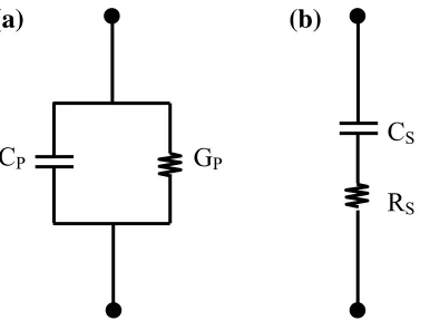
Figure 2-1. (a) Parallel equivalent circuit, and (b) series equivalent circuit of a device under
test (DUT) for the measurement using capacitance meters. ...27
Figure 2-2. Schematic circuit diagram of a capacitance-conductance meter []...28 Figure 2-3. Capacitance transient of a majority carrier trap (hole trap in this case) in a
Figure 2-4. Illustration of how a double boxcar integrator is used to define the emission rate
window. The output is the average difference of the capacitance amplitudes at the sampling times t1 and t2. The right-hand part of the figure is the so-called DLTS
spectrum [4]. ...31
Figure 2-5. (a)Band diagram of a p-type semiconductor with a transparent Schottky barrier
contact, which contains a minority carrier trap (ET); (b)Illumination through the barrier with a flux ΦO of photons (hv > Eg) generates electron-hole pairs at a rate
G(x) []. These generated charge carriers result in a drift current of holes, and drift and diffusion currents of electrons within the depletion region W. The higher density of electrons provides minority carriers for capture at the trap. ...34
Figure 2-6. Electron and hole concentrations in a reverse biased Schottky diode obtained
from solutions of the continuity equation: (----) semiconductor in the dark; (—) semiconductor illuminated. Inset: values of absorption coefficient α, lifetime τR,
and incident optical power density Φ0 used in the calculation []. ...37
Figure 2-7. Schematic of EBIC measurement on a Schottky barrier diode of p-type Si...38 Figure 2-8. (a) Schematic of the interaction between e-beam and bulk semiconductor. The
characteristic parameter of electron ranges Re is shown as the diameter of
electron-hole pairs generation volume; (b) Re as a function of the e-Beam energy. ...39
Chapter 3
Figure 3-1. Schematic of a strained-Si/SiGe/Si heterostructure, with most of the
dislocations confined within the SiGe graded layer, and some misfit dislocations generated at the strained-Si/SiGe interface. Note that some of the dislocations originate from the SiGe layer and penetrate up to the top Si layer...43
Figure 3-2. C-V characteristics of the Schottky barrier diodes measured in the temperatures ranging from 330 to 150 K. ...45
Figure 3-3. The depth profile of apparent carrier concentration of strained-Si/SiGe/Si
heterostructure, calculated from the C-V characteristics measured at 330K. ...46
Figure 3-4. (a) The schematic of the band diagram of a strained-Si/SiGe/Si heterostructure
with local high-concentration defects. This band diagram contains a Schottky barrier diode with a depletion capacitance CD, and a resistive graded SiGe layer represented by a capacitance CR in parallel with a resistance R. (b) The equivalent circuit for this band structure. ...49
Figure 3-5. The comparison of simulated (red lines) and measured (black lines) C-V
characteristics at 275 (a) and 225 K (b), respectively...52
Figure 3-6. An Arrhenius plot of resistance R as a function of (1000/T)...52 Figure 3-7. DLTS spectrum of the strained-Si/SiGe/Si heterostructure measured with
Chapter 4
Figure 4-1.C-V curves measured on as-grown and annealed samples at 300 K (solid lines)
and 100 K (dashed lines). ...62
Figure 4-2. Apparent charge carrier concentration profiles of as-grown (solid circles) and
annealed (open circles) heterostructures...62
Figure 4-3. Normalized DLTS spectra (∆C/C) measured in the as-grown heterostructure at
different depths. The biasing conditions are: VR= 0.5 V & VP = 0 V, VR= 1.0 V &
VP = 0.5 V, VR= 2.0 V & VP = 1.0 V, respectively. tP=1.0 ms...64
Figure 4-4. DLTS spectra measured in the annealed heterostructure using different pulse
durations tP(tP= 0.01, 0.03, 0.1 and 0.3 ms, respectively). Reverse voltage VR = 3.0 V, and pulse voltage VP = -0.3 V. ...64
Figure 4-5. DLTS peak height dependence on the pulse duration tP for defect H5 in the
annealed heterostructure. tP = 0.01, 0.03, 0.1, 0.3, 0.6 and 3 ms, respectively. Reverse voltage VR = 1.0 V, and pulse voltage VP = -0.3 V. ...67
Figure 4-6. EBIC micrographs of as-grown sample obtained at 20 keV (a) and 10 keV (b),
respectively. Image size is 100 × 100 µm2. Note that EBIC micrographs were obtained on the same sample location. ...71
Chapter 5
Figure 5-1. Dark-field Nomarski optical micrographs of etch pits delineated using
preferential etching for 15-nm-thick (a), and 73.5-nm-thick (b)
strained-Si/SiGe/Si heterostructures. ...81
Figure 5-2. MCTS spectra of as-grown 15-nm-thick strained-Si/SiGe/Si heterostructure
samples using an optical pulse of 1 ms for different reverse bias voltages VR. tW = 20 ms...82
Figure 5-3. MCTS spectra of as-grown 73.5-nm-thick strained-Si/SiGe heterostructure
samples for optical filling pulse durations tP of 0.1 s, 5 s, and 50 s. The reverse bias VR was kept at 0 V. tW = 20 ms. ...82
Figure 5-4. MCTS spectra measured on thermally-annealed sample, for different reverse
bias VR, while optical pulse duration tP= 0.1 ms, and emission rate e = 50 s-1. ...86
Figure 5-5. MCTS spectra measured on thermally-annealed sample. Dependence on the
optical filling pulse duration tP. The fixed parameters are the reverse bias VR= 1.0 V and emission rate e = 50 s-1...87
Figure 5-6. Dependence of normalized MCTS peak heights on the reverse bias voltage VR
for electron traps of different samples: the B lines of as-grown 15-nm-thick, and 73.5-nm-thick samples, the A, B, C lines of thermally-annealed 73.5-nm-thick sample. The theoretical curves for two ideal cases of uniform defect concentration, or defect located within the W-λ layer for VR of 0 V are also included for
INTRODUCTION
During the last 40 years, the amazing performance improvements in CMOS integrated
circuits are primarily driven by a continuous geometric scaling of individual MOSFET
transistors. As the device dimensions approach <100 nm, geometric scaling becomes
increasingly difficult. New materials that can improve the device performance are of great
interest. Strained-Si grown on a relaxed Si1-xGex buffer layer is becoming a promising
candidate to replace traditional bulk Si in high-performance CMOS, because of the enhanced
charge carrier mobilities for electrons and holes, as well as good compatibility to CMOS
fabrication technology.
Nevertheless, there are still many materials issues to be addressed, which are essential to
the successful application of the strained-Si CMOS technology. Although a metastable
strained-Si layer can be epitaxially grown at relatively low temperatures to a thickness larger
than the critical value predicted by Matthews-Blakeslee model, this metastable strained-Si
layer can relax by the formation of misfit dislocations at the strained-Si/SiGe interface, and
the rate of misfit dislocation formation increases exponentially with temperature. However,
the CMOS fabrication process includes standard steps (e.g., activation of ion-implanted
dopant species, and gate oxidation) requiring temperatures as high as 1000 ºC. Thus, it is
critical to be able to measure the changes of tensile strain and misfit dislocations density
during a high-temperature process.
Although various structural characterization methods (e.g., preferential etching, TEM,
strain relaxation and dislocation generation, there are limited efforts to study the electrical
properties of the extended defects generated at the strained-Si/SiGe interface, particularly
dislocation-related deep levels. It is obvious that the capability to detect dislocation-related
deep levels is critical to studying or even controlling the introduction of threading and misfit
dislocations, which can degrade the CMOS performance by increasing leakage current and
reducing the carrier mobility. The lack of electrical characterization results is mainly due to
the very small thickness (tens of nm) of top strained-Si layer, rendering the conventional
electrical junction based characterization techniques ineffective. Therefore, an in-depth study
of the electrically active defects within the strained-Si/SiGe/Si heterostructure, especially, the
strained-Si/SiGe interface, is carried out using conventional techniques (C-V, DLTS, and EBIC), as well as the unusual one like MCTS. The thesis is organized as following:
Chapter 1 of “Literature Review” discusses the conventional growth process of
strained-Si/SiGe/Si heterostructure and the reasons for carrier mobility enhancement. The
recent structural and electrical characterization results of defects of the strained-Si/SiGe/Si
heterostructure are included, and dislocation-related deep levels of plastically deformed n-type Si are reviewed.
Chapter 2 of “Research Methodology” briefly describes the electrical characterization
techniques used in this study (C-V, DLTS, MCTS, and EBIC), and the basic concept of
Schottky diodes for electrical testing. DLTS and MCTS are two powerful complementary
tools for studying deep levels located in the upper and lower halves of the band gap of a
semiconductor. EBIC with an e-beam of different energy can be used to study defects located
at different depths from the surface.
Strained-Si/SiGe/Si Heterostructure” focuses on the temperature-dependent C-V
characteristics of Schottky diodes of strained-Si/SiGe/Si heterostructure, and identifies
significant carrier depletion within the graded SiGe layer, which can be modeled as a
capacitance CR in parallel with resistance R. The agreement between the activation energy of resistance R and that of a hole trap level detected by DLTS indicates that the carrier depletion is caused by this defect level.
Chapter 4 of “Effects of Thermal Annealing on Deep-level Defects in
Strained-Si/SiGe/Si Heterostructure” studies the effects of thermal annealing at 800 ºC in
oxidizing atmosphere on the electrical properties of 73.5-nm-thick strained-Si/SiGe
heterostructure using C-V, DLTS and EBIC methods. DLTS technique identified a deep level located within 150 nm from the surface, introduced by the strain relaxation of top Si layer
during thermal annealing. The nature of this deep level is determined to be localized extended defect, i.e., point-defect clouds surrounding 60º dislocations from the dependence of DLTS
signal on electrical filling pulse duration.
Chapter 5 of “Minority Carrier Transient Spectroscopy Study of Strained-Si/SiGe/Si
Heterostructure” explores the applicability of MCTS technique for detecting defect levels
located within the strained-Si layer, or at the strained-Si/SiGe interface, using a laser pulse to
generate minority carriers within the depletion region of a Schottky diode. The observed
minority carrier (electron) defect levels of as-grown and annealed samples are then compared
with the well-known electron traps of plastically deformed n-type Si. One electron trap of as-grown sample is related to threading dislocations, and the high density electron traps of
thermally-annealed metastable sample are attributed to point-defects located at or close to
CHAPTER 1: LITERATURE REVIEW
1. 1. Strained-Silicon for Future CMOS
Strained-Si is a promising candidate to replace traditional bulk Si in deep submicron
complementary metal-oxide-semiconductor (CMOS) technology, due to the higher carrier
mobility. Also this outstanding material has very good compatibility to modern CMOS
fabrication processes. Essentially, it is now well established that without changing the channel
material, significant enhancements in device performance are possible using strained-silicon
[ 1 , 2 , 3 ]. Thus, the strained-Si wafer shows great promise and rapidly approaches its
practicality as an attractive candidate for fabricating high speed and low power CMOS
devices.
Figure 1-1. Schematic representation of the strain induced conduction band splitting in
strained-Si [2].
Theoretically, the reasons for carrier mobility enhancement in strained-Si have been
strain splits the six-fold degeneracy of the conduction band, and lowers the two-fold
degenerate perpendicular ∆-valleys with respect to the four-fold in-plane ∆-valleys in energy
space (see Figure 1-1 (a)). Such energy splitting suppresses inter-valley carrier scattering
between the two-fold and four-fold degenerate valleys, and causes preferential occupation of
the two-fold valleys, where the in-plane conduction mass is lower. These two effects lead to
increased electron mobility.
In unstrained Si, the valence band maximum is composed of three bands: the degenerate
heavy-hole (HH) and light-hole (LH) bands at k=0, and the split-off (SO) band which is
slightly lower in energy (see Figure 1-2 (a)). Similarly, the biaxial strain splits the valence
band degeneracy at the Γ-point and shifts the split-off band, and application of stress also
changes the shape of the bands, as shown in Figure 1-2 (b) [8]. Therefore, due to the band
deformation, the in-plane transport mass becomes smaller and the inter-band scattering is also
suppressed. Thus the in-plane hole mobility is improved.
Figure 1-2. Simplified schematic of hole valence band structure for (a) unstrained and (b)
1. 2. Strained-Si Channel
Strain in Si channel can be introduced in various ways. The two main techniques to
induce strain in a CMOS channel are global strain and local strain. Global strain requires a
virtual substrate upon which a strained layer is epitaxially grown. On the other hand, local
strain can be accomplished either by selectively growing pseudomorphic SiGe epitaxially in
recessed source-drain regions surrounding the channel, or by depositing highly-stressed
dielectric liners over the gate.
The focus of this thesis is on the electrical and structural properties of Si layer with
global strain, i.e., biaxial strain.
1.2.1. Growth of Strained-Si/SiGe/Si-substrate Heterostructure
Figure 1-3. A schematic diagram of the bulk lattice constants of a bulk-Si film to be grown on
top of a bulk-Si1−xGex film (a), and one of the two films placed together with the top film
being tensile strained (b).
The most commonly used method to induce global strain is to deposit a thin Si epitaxial
(a) (b)
layer on top of a thick relaxed SiGe buffer layer [2]. Silicon and germanium, both of the
diamond lattice structure, can form a continuous series of Si1-xGex alloy with x ranging from 0
to 1. The lattice constants are 0.5431 nm for Si and 0.5657 nm for Ge. And the lattice constant
aSiGe for relaxed Si1-xGex alloy could be calculated according to the Vegard’s law:
x
x
GeSi Ge
Si−x x
=
a
⋅
(
1
−
)
+
a
⋅
a
1 (Eq. 1. 1)Relaxed SiGe with 26% Ge has a crystal lattice parameter ~1% larger than that of Si.
Therefore, when a thin layer of Si is pseudomorphically grown on a thick, relaxed SiGe layer,
the lattice constant of the Si film conforms to that of the SiGe layer, and the lattice mismatch
between Si and SiGe leads to ~1% biaxial tensile strain in the Si layer, as shown in Figure 1-3.
The magnitude of the strain in the Si can be varied by changing the Ge content in the SiGe
template.
1. 3. Performance Enhancement of Strained-Si CMOS Devices
Strained-Si metal-oxide-semiconductor field-effect-transistor (MOSFETs) are device
structures that take advantage of strain-induced enhancement of carrier transport in silicon,
and the typical structures of strained-Si/relaxed SiGe bulk MOSFETs are shown in Figure 1-4.
Recent work has provided encouraging experimental data showing the mobility enhancement
with different devices structures, including both n-channel and p-channel devices. The
n-channel MOSFET mobility measured on large area, long channel devices are shown in
Figure 1-5, showing that the mobility of the strained-Si device is ~70% higher than the
universal MOSFET mobility or the mobility of the control Si device [10]. Fabrication
high temperature activation anneals are shown to have no adverse impact on device
characteristics, suggesting that a conventional CMOS process flow can be adopted while still
achieving the mobility and current drive enhancement.
Figure 1-4. Typical structures of strained-Si/relaxed SiGe bulk MOSFETs [9].
1. 4. Structural Characterization of Defects of Strained-Si/SiGe/Si Heterostructure
When producing strained layers for CMOS technology, constraints are imposed on the
thickness, lateral dimensions and crystalline quality of the channel layer. The foremost critical
challenge in the strained-Si/SiGe CMOS technology is the control of extended defects in the
epitaxial layers: dislocations. The defects present in the SiGe buffer layer also grow into the
strained-Si overgrown layer, and additional defects may be created in the strained-Si layer if
the thickness of the layer exceeds the critical thickness value. Thermal processing during
CMOS fabrication steps can cause relaxation of the strain in the Si layer, or out-diffusion of
Ge, and should be monitored accordingly.
1. 4. 1. Defects Structure of SiGe Buffer Layer
The primary function of the relaxed SiGe layer is to serve as a “virtual substrate” for
tensile-straining the top Si epilayer. In order to produce a relaxed SiGe epilayer with low
threading dislocation densities on a Si substrate, the conventional method is to grow thick (a
few µm) compositionally-graded buffer layers and a following layer of uniform SiGe.
Mismatch strain is gradually relaxed by a modified Frank–Reed (MFR) mechanism [11,12],
and the majority of 60° misfit dislocations (MDs) formed during the relaxation process are
trapped within the SiGe graded layer, as shown in Figure 1-6. These buried dislocations
should not greatly degrade MOSFET device performance at the strained-Si surface.
Some of these MDs, with a density of 105–106 cm-2, may thread to the MOSFET device
Figure 1-6. Cross-sectional TEM image of a strained-Si/SiGe heterostructure [13]. Most of
the dislocations are confined within the SiGe graded layer, while some misfit dislocations are generated at the interface of strained-Si and uniform SiGe layers.
1. 4. 2. Defects Structure of Strained-Si Top Layer
The choice of channel thickness in strained-Si MOSFETs is an important one. For the
strained-Si layer with a thickness in the thinnest regime of ~5 nm, carrier confinement will
decrease with decreasing thickness due to quantum effects. This poor confinement in the Si
channel leads to carrier conduction through the low-mobility relaxed SiGe buffer layer, and
degrades the overall device mobility [14]. In addition, thinner strained-Si layers are more
susceptible to Ge diffusion at high temperatures. For practical purposes, it is desirable to have
a strained-Si thickness of >15 nm, because 8-10 nm of the initial Si is typically consumed
1.4.2.1.Critical Thickness of Strained-Si Layer
Figure 1-7. Critical thickness hc of a silicon layer grown on a fully-relaxed Si1-xGex layer as a
function of the germanium content x [22].
The lattice mismatch between Si and relaxed Si1-xGex is ~4.2% x, where x is the Ge
content in the Si1-xGex layer. Since the lattice mismatch is sufficiently small, the deposited
first several atomic layers of Si will be strained to match the SiGe substrate and a coherent
interface will be formed. The strained-Si/SiGe heterostructure stores a high amount of elastic
strain energy, since the inter-atomic bond lengths in the epilayer are stretched or compressed
compared to their equilibrium values. At some thickness of an epilayer, generally called the
critical thickness hc, it becomes energetically favorable to relieve the elastic strain energy by introducing misfit dislocations and allowing the epilayer to relax towards its bulk lattice
constant. This critical thickness has been calculated by several groups based on different
models [15,16,17,18,19,20,21]. Figure 1-7 shows the calculated critical thickness of
exponentially decreasing value of the critical thickness with increasing strain, i.e., Ge content
[22].
As mentioned in Section 1.4.2, strained-Si thickness needs to be larger than 15 nm for practical purposes. Meanwhile, charge carrier mobilities of strained-Si grown on Si1-xGex
virtual substrates are theoretically predicted and experimentally demonstrated to increase with
higher Ge content because of a larger tensile strain, and saturate upon reaching a Ge content
of 25% for electrons [23,24,25], or 40% for holes [26,27,28,29], as shown in Table 1-1. Thus
there is a strong motivation to increase Ge content to the value of 40% to achieve maximum
carrier mobility enhancement of CMOS devices comprising of both n- and p-MOSFETs.
Since the combination of desired strained-Si layer thickness and Ge content exceeds the
theoretical curve of the critical thickness hc as a function of Ge content x, the critical thickness value becomes a restriction to the design of Si layer thickness and Ge content for
strained-Si/SiGe/Si MOSFETs. And the study of possible strain relaxation and dislocation
formation of a metastable strained-Si layer with a thickness exceeding hc becomes necessary to fully benefit from the strained-Si/SiGe/Si MOSFET architecture.
Table 1-1. Theoretical predicted values of low-field electron [23] and hole [26] mobility
enhancements of strained-Si layer grown on relaxed Si1-xGex layer, relative to the mobility
values of un-strained bulk-Si.
x 0.1 0.2 0.3 0.4 0.5
electron 1.46 1.68 1.70 1.70 1.70
hole 1.25 1.68 2.35 2.53 2.55
1.4.2 2. Strain Relaxation and Defect Formation for Strained-Si Layer
structural analysis techniques, e.g., preferential chemical etching, atomic force microscopy,
and transmission electron microscopy. It was generally accepted that TDs will glide as soon as
the thickness of the overgrown strained-Si exceeds the critical thickness hc, and result in the formation of MDs at the strained-Si/SiGe interface, according to the Matthews and Blakeslee
model [16,19]. Recent studies observed that dislocations may form in the strained-Si layers
even when the layer thickness is less than the predicted hc, via the nucleation of dislocation half-loops, in addition to the gliding of pre-existing threading dislocations [21]. The threading
dislocations connected to the misfit dislocations at the upper interface may extend into the
upper part of the constant SiGe layer, as shown Figure 1-6. Furthermore, stacking faults were
identified for the supercritical strained-Si layer, and related to the gliding of partial
dislocations [30,31]. Selective strain relaxation of strained-Si layer was also verified by
studying the strain fluctuation in the strained-Si/relaxed-SiGe heterostructure using
micro-Raman spectroscopy [32].
1. 5. Electrical Characterization of Defects of Strained-Si/SiGe/Si Heterostructure 1. 5. 1. Electrical Properties of Dislocated Si/SiGe/Si Layered Structures
The detrimental effects of dislocations on the electrical performance of devices
fabricated using Si/SiGe/Si heterostructures have been studied extensively. A correlation
between junction leakage current density and threading dislocation density (TDD) has been
established for both p-i-n diodes of Si0.75Ge0.25 graded buffer layers [33] and n+/p-junctions of
strained-silicon/relaxed Si0.8Ge0.2 [34]. The leakage was demonstrated to scale linearly with
the TDD, and can be modeled by deep-level assisted generation processes.
studied by measuring the leakage current of a metastable SiGe/Si p-n junction during heating
while monitoring the dislocation densities with in-situ TEM [35], or by comparing the
off-state leakage currents of strained-Si MOSFETs with various strained silicon thicknesses
(above or below the critical thickness) [36]. Thus, the increase of leakage current due to the
higher misfit dislocation density has also been established, and the leakage mechanism
between source/drain contacts of strained-Si MOSFET was further studied using photon
emission microscopy, and shown to be the enhanced dopant diffusion near misfit dislocations,
as shown in Figure 1-8 [36].
Figure 1-8. Photon emission microscopy images of light emission from strained-silicon
MOSFETs with varying strained-Si layer thickness. The differences between light emission for different strained-Si thickness supports the hypothesis that misfit dislocation diffusion pipes cause source/drain shorts [36].
Furthermore, the introduction of misfit dislocations at the strained-Si/SiGe interface will
substantially degrade the expected mobility enhancement of strained-Si layer. In addition to
the mobilities reduction due to the loss of tensile strain, misfit dislocations also induce a
strong scattering potential close to the carriers in the strained-Si, and disadvantageously affect
In short, the introduction of dislocations (TDs or MDs) within, or even close to the
strained-Si top layer would be detrimental to the final strained-Si MOSFETs device
performance, by lowering the charge carrier mobility, as well as increasing the off-state
leakage currents. Hence, it is essential to perform both structural and electrical
characterizations of dislocations at the strained-Si/SiGe interface, and especially desirable to
be able to non-destructively detect the strain-relaxation of metastable strained-Si layer during
the CMOS fabrication process.
The device performance enhancement due to higher carrier mobilities, and the possible
degradations because of extended defects have also been mentioned in the most recent 2004
International Technology Roadmap for Semiconductors (ITRS) published by the Semiconductor Industry Association (SIA), as shown in Table 1-2 of the information related to
strained-Si MOSFETs [38].
Table 1-2. The information related to strained-Si MOSFETs in 2004 International Technology Roadmap for Semiconductors (ITRS) [38].
Transport-enhanced MOSFETs
Advantages Potential Weakness
Strained Si, Ge, SiGe, SiGeC or other semiconductor; on bulk or SOI
High mobility without change in device architecture
Material defects and diode leakage;
Process compatibility and thermal budget.
1. 5. 2. Electrical Defect Characterization of Dislocations in Strained-Si Top Layer
So far, several studies have been done concerning the defect states within the strained-Si
top layer employing electrical characterization tools [39,40].Yuan et al. have demonstrated that electron-beam-induced current (EBIC) technique can be used to investigate MDs at the
contact [39]. Misfit dislocations were intentionally introduced to the top strained-Si layer by
growing the strained-Si layer to a thickness larger than the critical thickness. Misfit
dislocations located at different depths (at the strained-Si/SiGe interface, or within the graded
SiGe layer) can be differentiated by using e-beam of different energy for EBIC measurements.
For an e-beam of 4 keV (or 20 keV), the electron range Re is calculated to be 320 nm (or 3.5
µm), meaning that the volume of generated electron hole pairs contains either only strained-Si
and constant SiGe layers for 4 keV, or strained-Si constant and graded SiGe layers for 20 keV.
Figure 1-9 illustrates typical EBIC micrographs taken with an e-beam of 4 keV at 300 K (a)
and 65 K (b), or with an e-beam of 20 keV at 300 K (c) and 65 K (d), respectively.
Low-temperature EBIC micrograph of strained-Si and constant SiGe layers (Figure 1-9(b))
shows two orthogonal sets of dark lines oriented along 〈110〉 directions and some dark dots,
originating from the misfit and threading dislocations at the strained-Si/SiGe interface; while
low-temperature EBIC micrograph of the graded SiGe layer (Figure 1-9(d)) shows a dense
orthogonal dark line pattern of the dense dislocation network.
Since little or no EBIC contrast is observed on the same sample region at 300 K (see
Figure 1-9(a) and (c)), the energy level of observed dislocations could be estimated to be
10 µm
(a)(d) (c)
(b)
Figure 1-9. EBIC micrographs of 100-nm-thick strained-Si/Si0.8Ge0.2/Si heterostructure: (a) 4
keV at 300 K; (b) 4 keV at 65 K; (c) 20 keV at 300 K; (d) 20 keV at 65 K [39].
Wang et al. used DLTS and metal-oxide-semiconductor (MOS) transient capacitance
methods to evaluate the interface states density of both oxide/strained-Si and strained-Si/SiGe
interfaces and minority carrier generation lifetime of a MOS structure, respectively [43]. It
was found that interface state density is independent on the thickness of strained-Si, and
strongly increases with higher Ge content of SiGe layer. On the other hand, minority carrier
generation lifetime shows an obvious dependence on both strained-Si thickness and Ge
1. 5. 3. Dislocation-related Deep Levels
Despite the obvious importance of studying dislocation-related deep levels within the
strained-Si/SiGe/Si heterostructure, there is still a lack of understanding of the
electrically-active defects located within the top strained-Si layer, or at the strained-Si/SiGe
interface, critical to the optimum performance of final MOSFETs. This situation is mainly due
to the very small thickness (tens of nm) of top strained-Si layer, rendering the conventional
electrical junction based characterization tools ineffective. For this reason, this thesis focuses
on the electronic defect characterization of strained-Si/SiGe/Si heterostructure, employing a
combination of electrical (C-V, DLTS, MCTS, and EBIC), and structural (preferential
etching/Nomarski optical microscopy) characterization techniques.
Although no direct results on the defect states within the strained-Si layer are available
in the literature, there are extensive works on plastically deformed Si and SiGe/Si
heterostructure, producing a large body of results about dislocation-related deep levels in Si or
SiGe. Since both strain-relaxation of metastable strained-Si layer and plastic deformation of
bulk Si involve the generation of dislocations, the previous extensive work on plastically
deformed Si will be used as references for the discussion of defects detected in the
strained-Si/SiGe/Si heterostructure. In the following, the deep levels of plastically deformed
Si will be briefly mentioned.
1.5.3.1 Defect states in plastically deformed silicon
DLTS has been extensively applied to plastically deformed silicon to study the electronic
properties of a complex spectrum of extended defects by several groups [44,45,46,47,48].
along the [112] direction in a forming gas atmosphere (92% N2 and 8% H2) using a quartz
and graphite deformation apparatus. The resulting plastic strain ranges from 1% to 1.5%. In
addition to dislocations, a large amount of point defects and point-defect clusters are
introduced through the dislocation motion or interaction, during the plastic deformation
process. Consequently, both donor and acceptor states are generated within the band gap, due
to these electrically active lattice imperfections. The complex defect spectrum of plastically
deformed n-type Si has been identified as four traps, labeled A, B, C, and D, mainly based on the extensive work on the formation and annealing behaviors of different defects [45, 48], as
shown in Figure 1-10, and their characteristic parameters are reported in Table 1-3.
Figure 1-10. DLTS spectra of a plastically deformed n-type Si with a dislocation density of
Table 1-3. Electrical parameters of electron traps in plastically deformed n-type silicon,
including trap energy level within the energy band gap, and capture cross section [45,48].
Trap Ea (eV) σn (cm2)
A 0.19
B 0.29 1.5×10⁻¹⁶
C 0.40 8.9×10⁻¹⁶
D 0.56
Moreover, several unique properties of dislocation-related defect states have been
identified using DLTS technique, and will be briefly mentioned in the following:
(1) Dislocations are spatially extended defects, and consequently they can change their
charge state within wide limits by capturing or emitting many electrons.
(2) Due to the strain field associated with dislocations, the capacitance transients are
often non-exponential, resulting in broadened DLTS peaks.
(3) Coulomb interaction among charges confined at the dislocation results in a
time-dependent Coulomb barrier Φ(t), which builds up during the capture process of charge carriers. The presence of the Coulomb barrier around the dislocation causes the ‘‘logarithmic
filling time dependence’’ of extended defects, and the local band bending may also induce a
shift of the dislocation level with respect to the Fermi level, during filling and emptying of the
traps.
After extensive studies on the formation and annealing behaviors of different defects, as
well as computer simulations, the general conclusion about the origin of the deep levels of
plastically-deformed n-type Si detected by DLTS technique is that the electrical properties are mainly due to point defect effects, not the dislocation core structure. And more specifically,
1. 6. References
______________________________________________________________________________________
1 T. Vogelsang, and K. R. Hofmann, Appl. Phys. Lett. 63, 186 (1993).
2 K. Rim, J. L. Hoyt, and J. F. Gibbons, IEEE Trans. Elect. Dev. 47, 1406 (2000).
3 T. Tezuka, N. Sugiyama, and S. Takagi, Appl. Phys. Lett. 79, 1798 (2001).
4 M. V. Fischetti and S. E. Laux, J. Appl. Phys. 80, 2234 (1996).
5 S. Takagi, J. L. Hoyt, J. J. Welser, and J. F. Gibbons, J. Appl. Phys. 80, 1567 (1994).
6 J. B. Roldan, F. Gamiz, J. A. Lopez-Villanueva, and J. E. Carceller, J. Appl. Phys. 80, 5121
(1996).
7 R. Oberhuber, G. Zandler, and P. Vogl, Phys. Rev. B 58, 9941 (1998).
8 D. K. Nayak, J. C. S. Woo, J. S. Park, K. L. Wang, and K. P. MacWilliams, Appl. Phys. Lett.
62, 2853 (1993).
9 K. Rim, et al., Solid-State Elect. 47, 1133 (2003).
10 K. Rim, S. Koester, M. Hargrove, J. Chu, P. M. Mooney, J. Ott, T. Kanarsky, P. Ronsheim, M. Ieong, A. Grill, and H.-S. P. Wong, Symposium on VLSI Technology, p. 59-60 (2001). 11 E. A. Fitzgerald, Y.-H. Xie, D. Monroe, P. J. Silverman, J. M. Kuo, A. R. Kortan, F. A.
Thiel, and B. E. Weir, J. Vac. Sci. Technol. B 10, 1807 (1992).
12 F. K. LeGoues, B. S. Meyerson, J. F. Morar, and P. D. Kirchner, J. Appl. Phys. 71, 4230
(1992).
13 X. L. Yuan, T. Sekiguchi, S. G. Ri, and S. Ito, Eur. Phys. J. Appl. Phys. 27, 337 (2004).
14 M. T. Currie, C. W. Leitz, T. A. Langdo, G. Taraschi, E. A. Fitzgerald, and D. A. Antoniadis, J. Vac. Sci. Technol. B 19, 2268 (2001).
15 J. H. Van der merwe, J. Appl. Phys. 34, 123 (1963).
16 J. W. Matthews, and A. E. Blakeslee, J. Cryst. Grow. 27, 118 (1974).
17 J. W. Matthews, J. Vac. Sci. Technol. 12, 126 (1975).
18 D. J. Eaglesham, E. P. Kvam, D. M. Maher, C. J. Humphreys, G. S. Green, B. K. Tanner, and J. C. Bean, Appl. Phys. Lett. 53, 2083 (1988).
19 R. People, and J. C. Bean, Appl. Phys. Lett. 47, 322 (1985).
20 J. C. Bean, L. C. Feldman, A. T. Fiory, S. Nakahara, and I. K. Robinson, J. Vac. Sci. Technol. A, 2, 436 (1984).
21 S. B. Samavedam, W. J. Taylor, J. M. Grant, J. A. Smith, P. J. Tobin, A. Dip, A. M. Phillips, and R. Liu, J. Vac. Sci. Technol. B 17, 1424 (1999).
22 D. K. Sadana, S. W. Bedell, A. Reznicek, J. P. de Souza, K. E. Fogel and H. J. Hovel, Proceedings of Electrochem. Soc. Meet. 501, 719 (2006).
23 S. Takagi, J. L. Hoyt, J. J.Welser, and J. F. Gibbons, J. Appl. Phys. 80, 1567 (1996).
24 J. Welser, J. L. Hoyt, S. Takagi, and J. F. Gibbons, Tech. Dig. - Int. Electron Devices Meet.
1994, 373.
27 M. V. Fischetti and S. E. Laux, J. Appl. Phys. 80, 2234 (1996).
28 D. K. Nayak, K. Goto, A. Yutani, J. Murota, and Y. Shiraki, IEEE Trans. Electron Devices
43, 1709 (1996).
29 K. Rim et al., Symposium on VLSI Technology, Honolulu, Hawaii, 2002 (IEEE,
Piscataway, NJ, 2002), p. 98.
30 S. W. Bedell, K. Fogel, D. K. Sadana, H. Chen, and A. Domenicucci, Appl. Phys. Lett. 85, 2493 (2004).
31 Y. Kimura, N. Sugii, S. Kimura, K. Inui, and W. Hirasawa, Appl. Phys. Lett. 88, 031912
(2006).
32 K. Sawano, S. Koh, Y. Shiraki, N. Usami, and K. Nakagawa, Appl. Phys. Lett. 83, 4339
(2003).
33 L. M. Giovane, H. –C. Luan, A. M. Agarwal, and L. C. Kimerling, Appl. Phys. Lett. 78,
541 (2001).
34 G. Eneman, E. Simoen, R. Delhougne, P. Verheyen, R. Loo, and K. De Meyera, Appl. Phys. Lett. 87, 192112 (2005).
35 F. M. Ross, R. Hull, D. Bahnck, J. C. Bean, L. J. Peticolas, and C. A. King, Appl. Phys. Lett. 62, 1426 (1993).
36 J. G. Fiorenza, G. Braithwaite, C. W. Leitz, M. T. Currie, J. Yap, F. Singaporewala, V. K. Yang, T. A. Langdo, J. Carlin, M. Somerville, A. Lochtefeld, H. Badawi, and M. T. Bulsara, Semicond. Sci. Technol. 19 L4 (2004).
37 K. Ismail, F. K. LeGoues, K. L. Saenger, M. Arafa, J. O. Chu, P. M. Mooney, and B. S. Meyerson, Phys. Rev. Lett. 73, 3447 (1994).
38 Semiconductor Industry Association, International Roadmap for Semiconductors 2004
Edition (International SEMATECH, Austin, TX 2004).
39 X. L. Yuan, T. Sekiguchi, S. G. Ri, and S. Ito, Appl. Phys. Lett. 84, 3316 (2004).
40 D. Wang, M. Ninomiya, M. Nakamae, and H. Nakashima, Appl. Phys. Lett. 86, 122111
(2005).
41 M. Kittler, C. Ulhaq-Bouillet, and V. Higgs, J. Appl. Phys. 78, 4573 (1995).
42 V. Kveder, M. Kittler, and W. Schroter, Phys. Rev. B 63, 115208 (2001).
43 D. Wang, M. Ninomiya, M. Nakamae, and H. Nakashima, Appl. Phys. Lett. 86, 122111
(2005).
44 L. C. Kimerling, and J. R. Patel, Appl. Phys. Lett. 34, 73 (1979).
45 P. Omling, E.R. Weber, L. Montelius, H. Alexander, J. Michel, Phys. Rev. B, 23, 6571
(1985).
46 C. Kisielowski, and E. Weber, Phys. Rev. B 44, 1600 (1991).
47 W. Schröter, J. Kronewitz, U. Gnauert, F. Riedel, and M. Seibt, Phys. Rev. B 52, 13726,
(1995).
CHAPTER 2: RESEARCH METHODOLOGY
2. 1. Introduction
In this thesis, various structural and electrical characterization methods were employed
to study different aspects of the strained-Si/SiGe/Si heterostructures, with focuses on the top
strained-Si layer. Threading and misfit dislocations were delineated using preferential etching,
and observed by a Nomarski optical microscope. Plan-view and/or cross-sectional
transmission electron microscopy (TEM) were used to study the distribution of dislocations
within the heterostructures.
The focus of this study is the electronic defect characterization of trap levels related to
the top strained-Si layer. For the graded-SiGe layer, temperature- and frequency-dependent
capacitance-voltage (C-V) measurements were employed to study the effects of high density of dislocations on the capacitance values of Schottky diodes fabricated using
strained-Si/SiGe/Si heterostructures. Deep-level transient spectroscopy (DLTS) and minority
carrier transient spectroscopy (MCTS) are two powerful complementary tools for studying
deep levels located in the upper and lower halves of the band gap of a semiconductor. MCTS
technique uses laser pulse to excite minority carriers within the depletion region of a Schottky
diode to fill trap levels, and then monitor the emission of minority carriers from the trap levels
when the laser is turned off. Thus MCTS is well suited for studying near-surface defects (e.g.,
the strained-Si/SiGe interface). Electron-beam induced current (EBIC) using an e-beam of
different energy can be used to detect defects located at different depths from the surface, and
can be used to separate the defect levels related to the top strained-Si layers and deeper graded
experimental procedures employed in this study.
2. 2. Schottky Barrier Diodes
When a metal and a semiconductor are brought into intimate contact with each other, a
rectifying contact (Schottky barrier diode) can be formed. An energy barrier (Schottky barrier)
arises due to the difference in the work functions of the metal and semiconductor. Though the
details of Schottky barrier formation are not yet fully understood, it was pointed out that
imperfections at the semiconductor surface (surface states) play an important role in
determining the barrier height, which is relatively independent of the work function of the
metal [1]. As a result of the equilibration of Fermi levels in both materials, a semiconductor
region depleted of free carriers forms near the contact, and this depletion region or space
charge region (SCR) is accompanied by a band bending due to the ionized dopant impurities.
Using the thermionic emission theory and neglecting series and shunt resistance, the
Schottky barrier current-voltage characteristics are described by
⎟ ⎟ ⎠ ⎞ ⎜ ⎜ ⎝ ⎛ − ⎟⎟ ⎠ ⎞ ⎜⎜ ⎝ ⎛
= exp 1
kT n qV I I I
S , (Eq. 2. 1)
where IS, the dark saturation current, is given by
⎟ ⎠ ⎞ ⎜ ⎝ ⎛ Φ − = ∗ kT q T AA I B
S 2exp
. (Eq. 2. 2)
Here, q is the charge of an electron, A is the diode area, A* is the effective Richardson’s constant, nI represents the ideality factor and ΦB is the Schottky barrier height.
equation, the following equations relating to the depletion width and free carrier concentration
can be derived:
(
)
B s A N
q dV C d 2 0 2 2 1 ε ε − = /
, (Eq. 2. 3)
C A
W = εsε0 , (Eq. 2. 4)
where εs is the dielectric constant of the semiconductor, ε0 is the permittivity of free space, C
is the capacitance, NB (=NA or ND, depending on doping type) is the free carrier concentration and W is the depletion width.
The above two equations are only applicable to semiconductors in which the deep level
trap concentrations are relatively low in comparison to the dopant concentration. If there are
traps present in sufficiently high concentrations, the measured free carrier profiles are no
longer representative of the dopant concentration since the deep levels are able to contribute
to the measured capacitance.
2. 3. Capacitance-Voltage (C-V) Measurement
The capacitance-voltage measurement is a fundamental but very important technique to
assess the electrical properties of a dielectric film or a device. Capacitance can be defined as
the change in the charge amount, dQ, due to a change in the voltage, dV:
dV dQ
C = . (Eq. 2. 5)
This method is known as differential or small signal capacitance. Most capacitance
superimposing a small-amplitude ac voltage v on the dc voltage V, as a change of voltage. Capacitance meters assume the device under test (DUT) to be represented by either the
parallel equivalent circuit in Figure 2-1 (a) or the series equivalent circuit in Figure 2-1 (b).
Figure 2-1. (a) Parallel equivalent circuit, and (b) series equivalent circuit of a device under
test (DUT) for the measurement using capacitance meters.
For the DUT represented by a parallel equivalent circuit (see Figure 2-2), an ac signal vi
is applied to the DUT and the device impedance Z is calculated from the ratio of vi to the sample current ii. In the vector voltage-current method, the ac voltage typically varies at frequencies of 10 kHz to 1MHz with amplitude of 10 to 20 mV. Since the high input
impedance of a high-gain operational amplifier allows no current through (ii ≈ io), the
amplifier with a feedback resistor RF operates as a current-to-voltage converter: io = -vo/RF.
Since ii = vi/Z, the device impedance can be derived from vo and vi as
o i F
v v R
Z =− . (Eq. 2. 6)
For the parallel equivalent circuit in Figure 2-2, the device impedance of the is given by
CP GP
CS
RS
2 2
2
2 ( ) G ( C) C j c
G G Z
ω ω
ω − +
+
= , (Eq. 2. 7)
where C is the equivalent parallel capacitance, G is the equivalent parallel conductance, and the testing angular frequency ω = 2πf. The device impedance consists of a conductance and a susceptance, respectively. Furthermore, the voltages vo and vi are fed to a phase detector and the conductance and susceptance of the sample are obtained by using the 0º and 90º phase
angles of vo referenced to vi. The 0º phase angle gives the conductance G while the 90º phase angle gives the susceptance or the capacitance C.
Figure 2-2. Schematic circuit diagram of a capacitance-conductance meter [2].
2. 4. Deep-Level Transient Spectroscopy (DLTS)
For an ideal Schottky barrier diode of p-type silicon under the depletion approximation, there is no possibility of carrier capture. Thus only the emission process can be observed,
which can only happen through the forced introduction of carriers, by applying a voltage bias
pulse. When carriers leave the filled deep states due to an external influence, a capacitance
structures will be considered.
2. 4. 1. Capacitance Transient
Let us consider a deep level hole trap situated at an energy ET within the semiconductor band gap with a concentration of NT states per unit volume. Figure 2-3 (a)-(c) illustrate the capture and emission processes of majority carriers (holes are symbolized by open circles) by
this deep level, when the voltage bias of the Schottky diode is pulsed. Initially, the device is
under reverse bias VR. In this condition, no mobile carriers are present in the SCR of width W.
The deep level states within the band gap in that region are therefore empty (or filled with
electrons) as symbolized by the filled circles.
Immediately after an injection pulse towards zero bias, the SCR decreases and majority
carriers are then available for capture. The filled majority carrier traps are represented by the
open circles.
Once the injection pulse is switched off and the device returned to its initial state, the
junction capacitance is reduced due to the trapped majority carriers compensating the
immobile charged states in the SCR. These carriers can be excited into the valence band EV, and swept away from the SCR by the applied voltage potential, provided there is sufficient
excitation energy to stimulate such transitions. This excitation energy can either be in the form
of thermal or optical energy. The emission rate ep of a hole from a deep level at a temperature
T is described by
⎟ ⎠ ⎞ ⎜
⎝
⎛ −
− =
kT E E K
T
e T V
p
p exp
2
Here σp is the hole capture cross-section, k is the Boltzmann constant, and K is a material
coefficient which is dependent on both doping types and semiconductor materials.
Figure 2-3. Capacitance transient of a majority carrier trap (hole trap in this case) in a p-type
Schottky barrier diode. The diode (a) is under reverse bias VR, (b) injected with a filling pulse
VP, and (c) is again at VR where the carriers are emitted by the majority carrier trap [3].
The resulting junction capacitance can then be expressed by an exponential time-varying
function as
(
t ep)
Ct C
t
C ⎟= − ⋅
⎠ ⎞ ⎜ ⎝ ⎛−
= (0)exp (0)exp )
(
τ , (Eq. 2. 9)
C(0) is the capacitance at t = 0, the instant the forward pulse is switched off and the
capacitance transient begins.
The capacitance transient forms the basis of the DLTS technique, and can be used to
extract the electronic properties of deep levels.
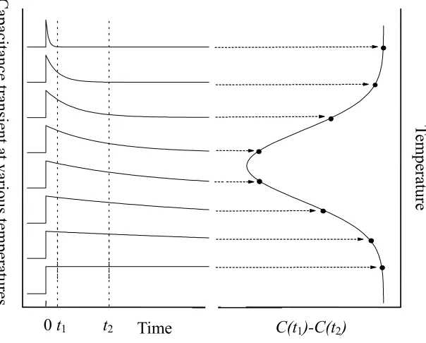
2. 4. 2. DLTS Signal Using a Rate Window
Figure 2-4. Illustration of how a double boxcar integrator is used to define the emission rate
window. The output is the average difference of the capacitance amplitudes at the sampling times t1 and t2. The right-hand part of the figure is the so-called DLTS spectrum [4].
The main feature of the DLTS technique is the employment of an instrument to set an
emission rate window such that the instrument produces a maximum signal output
proportional to the defect concentration when the emission rate of carriers from the trap falls
within the set rate window. To produce what is commonly known as a DLTS spectrum, the
Capacitan
ce trans
ient at various temperatu
res
Te
m
per
at
ur
e
diode is set at a reverse bias VR on top of which is superimposed a continuous train of positive filling pulses VP, while the temperature T is ramped. When the carriers have enough thermal energy, emission from the trap will take place. Figure 2-4 illustrates how the original rate
window, using a double boxcar, was implemented [4]. The boxcar samples the capacitance at
two fixed times t1 and t2 after the start of the capacitance transient, and determines the
corresponding change in the capacitance ∆C. The emission rate time constant τ of the carriers
from the defect is varied by changing the temperature.
A maximum appears in the ∆C output at a certain temperature Tmax, when τ is related to
t1 and t2 through the formula
) / ln( 2 1
1 2 t t t t − =
τ . (Eq. 2. 10)
Tmax is unique for each trap at a given τ. By performing further temperature scans using
different rate windows, a set of Tmax corresponding to each τ for the same trap can be
generated.
By rearranging Eq. 2.8, one obtains
(
)
ln( )ln ln max 2 max 2 max p a K kT E T e
T τ σ
− = ⋅ = ⎟⎟ ⎠ ⎞ ⎜⎜ ⎝ ⎛
, (Eq. 2. 11)
where Ea and σp represents the apparent activation energy and apparent capture
cross-section, respectively. Thus, an Arrhenius plot can then be produced from this set of
values, to extract the values of apparent activation energy and capture cross-section of a deep
2. 4. 3. Determination of Concentration of Trap Level
The concentration of a specific trap can be directly determined by observing the change
in capacitance as a function of the region being sampled. If the doping profile NA and trap level concentration NT are spatially uniform for p-type material, and NT is much lower than NA, then the defect concentration NT is given by the following approximation
2 2 2 ) ( ) ( 2 λ λ − − − ∆ = P R R A T W W W C C N
N , (Eq. 2. 12)
where ∆C is the capacitance transient amplitude (given by the height of a DLTS peak), and C
is the capacitance under the applied reverse bias voltage VR. WR and WP are the depletion region widths for the reverse bias (VR) and the filling pulse (VP) voltages, respectively. λ is the length of the transition region in the depletion region where the deep level lies above the
Fermi level.
To a first approximation, if we can further assume that ∆C << C, and λ << WP (all traps are completely filled during the filling pulse), then the defect concentration NT is given by
A
T N
C C N ≈∆ ×2
. (Eq. 2. 13)
This equation typically underestimates the true trap density since the pulse used to fill the
traps does not encompass the entire depletion region.
2. 5. Minority Carrier Transient Spectroscopy (MCTS)
DLTS technique employing electrical pulsing is limited to the characterization of defect
states in only one half of the band gap. To study the defect states throughout the whole band
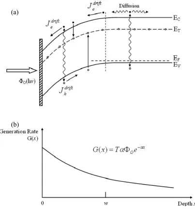
al. [5]. Laser pulse with photon energy greater than the band gap (hv > Eg) is directed to a semitransparent Schottky barrier diode to generate electron-hole pairs within the
semiconductor. Figure 2-5(a) shows the band diagram of a semi-transparent Schottky barrier
diode on a p-type semiconductor with a reverse bias of VR.
Figure 2-5. (a)Band diagram of a p-type semiconductor with a transparent Schottky barrier
contact, which contains a minority carrier trap (ET); (b)Illumination through the barrier with a flux ΦO of photons (hv > Eg) generates electron-hole pairs at a rate G(x) [6]. These generated
(a)
within the depletion region W. The higher density of electrons provides minority carriers for capture at the trap.
Illumination through the barrier with a flux ΦO of photons (hv > Eg) generates electron-hole pairs, as illustrate in Figure 2-5(b). Electrons (or holes) are generated at a local
rate per unit volume G(x)
x O
C e
T x
G( )= αΦ −α , (
Eq. 2. 14)
where TC is the transparency of the contact, α is the absorption coefficient at the particular photon energy.
Within the depletion region W, the electric field E acts on both electrons and holes to produce a drift current: holes drift in a positive x direction into the semiconductor, and electrons in a negative x direction toward the metal, as shown in Figure 2-5(a). Furthermore,
the electric field prevents holes generated beyond W from entering the depletion region,
whereas draws electrons into the depletion region. Within the depletion region, the electron
current is made up of drift and diffusion components, whereas the hole current is due to drift
alone. Thus, the steady state electron concentration exceeds the hole concentrations, and the
ratio of minority carrier to majority carrier within the depletion region can be further
improved by increasing the electron diffusion current using a semiconductor with a long
diffusion length.
Consequently, within the depletion region W, only minority carriers are available for capture at traps during the optical pulse. When the laser pulse is turned off, the subsequent
thermally-stimulated electron emission transient from the trap level is measured and processed
![Figure 1-4. Typical structures of strained-Si/relaxed SiGe bulk MOSFETs [9].](https://thumb-us.123doks.com/thumbv2/123dok_us/1401078.1172771/20.612.170.438.425.642/figure-typical-structures-strained-relaxed-sige-bulk-mosfets.webp)
![Figure 1-6. Cross-sectional TEM image of a strained-Si/SiGe heterostructure [13]. Most of the dislocations are confined within the SiGe graded layer, while some misfit dislocations are generated at the interface of strained-Si and uniform SiGe layers](https://thumb-us.123doks.com/thumbv2/123dok_us/1401078.1172771/22.612.152.466.77.332/sectional-strained-heterostructure-dislocations-dislocations-generated-interface-strained.webp)
![Figure 1-7. Critical thickness hc of a silicon layer grown on a fully-relaxed Si1-xGex layer as a function of the germanium content x [22]](https://thumb-us.123doks.com/thumbv2/123dok_us/1401078.1172771/23.612.151.466.103.327/figure-critical-thickness-silicon-relaxed-function-germanium-content.webp)
![Figure 1-9. EBIC micrographs of 100-nm-thick strained-Si/Si0.8Ge0.2/Si heterostructure: (a) 4 keV at 300 K; (b) 4 keV at 65 K; (c) 20 keV at 300 K; (d) 20 keV at 65 K [39]](https://thumb-us.123doks.com/thumbv2/123dok_us/1401078.1172771/29.612.165.482.79.399/figure-ebic-micrographs-thick-strained-heterostructure-kev-kev.webp)
![Figure 1-10. DLTS spectra of a plastically deformed 10n-type Si with a dislocation density of 4 cm-2, before (solid line) and after (dashed line) thermal annealing at 850 ºC for 1 h [48]](https://thumb-us.123doks.com/thumbv2/123dok_us/1401078.1172771/31.612.152.467.350.603/figure-spectra-plastically-deformed-dislocation-density-thermal-annealing.webp)
![Table 1-3. Electrical parameters of electron traps in plastically deformed n-type silicon, including trap energy level within the energy band gap, and capture cross section [45,48]](https://thumb-us.123doks.com/thumbv2/123dok_us/1401078.1172771/32.612.125.489.117.195/electrical-parameters-electron-plastically-deformed-including-capture-section.webp)