Area–Delay–Power Efficient Carry-Select
Adder
Sareeka Tulshiram Deore, Prof. Dr. P. Malathi
M.E. Student, Dept. of E&TC, D.Y.Patil College of Engineering, Akurdi, Pune, India
Vice-Principal, Dept. of E&TC, D.Y.Patil College of Engineering, Akurdi, Pune, India
ABSTRACT: Carry Select Adder (CSLA) is faster than any other adders used in many data-processing processors to perform arithmetic functions speedily.In adder design carry generation is the critical path. To reduce the power consumption of data path we need to reduce Area and Delay of the adder.The proposed design is implemented without using multiplexer and RCA structure with Cin=1. Instead of multiplexer and RCA Cin=1 structure hear we used simple combinational circuit which consists AND and XOR and OR gates.In the proposed scheme, the carry select (CS) operation is scheduled before the calculation of final-sum, which is different from the conventional approach.Bit patterns generated by two carry words and fixed carry cin is used by CS unit.The proposed CSLAdesign involves significantly less area and delay than the recently proposed BEC-based CSLA.A theoretical estimate shows that the proposed SQRT-CSLA involves nearly 35% less area–delay–product (ADP) than the BEC-based SQRT-CSLA, which is best among the existing SQRT-CSLA designs, on average, for different bit-widths. Carry Select Adder (CSLA) is one of the fastest adders used in many data-processing processors to perform fast arithmetic functions.The proposed design is synthesized and simulated in Xilinx ISE design suite 14.2 and is implemented on Spartan 6 XC6SLX16 CSG324 FPGA device.
KEYWORDS: Adder, arithmetic unit, SQRT, CSLA, FPGA, BEC.
I. INTRODUCTION
Low power, area-efficient, and high-performance VLSI systems are increasingly used inelectronic applications such as portable mobile devices, multi standard wireless receivers, and biomedical instrumentation [1], [2]. An adder is the main component of an arithmetic unit. A complex digital signal processing (DSP) system involves several adders. Applications where these are used are multipliers, DSP to execute various algorithms like FFT, FIR and ITR. In microprocessors, millions of instructions per second are performed. An efficient adder design essentially improves the performance of a complex (CS) methods have been suggested to reduce the CPD of adders. A conventional carry select adder (CSLA) is consist of an RCA–RCA configuration it uses multiple pairs of Ripple Carry Adders(RCA) to generate partial sum and carry by considering carry input Cin=O and Cin= I , then the final sum and carry are selected by the multiplexers (mux)[3]. A ripple carry adder (RCA) uses a simple design, but carry propagation delay (CPD) is the main concern in this adder. A conventional CSLA has less CPD than an RCA, but the design is not attractive since it uses a dual RCA. Few attempts have been made to avoid dual use of RCA in CSLA design. Kim and Kim [4] used one RCA and one add-one circuit instead of two RCAs, where the add-one circuit is implemented using a multiplexer (MUX). He et al. [5] proposed a square-root (SQRT)-CSLA to implement large bit-width adders with less delay. In a SQRT CSLA, CSLAs with increasing size are connected in a cascading structure. The main objective of SQRT-CSLA design is to provide a parallel path for carry propagation that helps to reduce the overall adder delay. Ramkumaret.al proposed BEC technique by using (n+1)-bit BEC instead of n-bit RCA with Cin=1 which reduces the area power-delay product and total power consumption with slight increase in delay [6].
redundant operations in the formulation, whereas adder delay mainly depends on data dependence. In the existing designs, logic is optimized without giving any consideration to the data dependence.
Based on the proposed logic formulation, we have derived an efficient logic design for CSLA. Due to optimized logic units, the proposed CSLA involves significantly less ADP than the existing CSLAs. We have shown that the SQRT-CSLA using the proposed SQRT-CSLA design involves nearly 32% less ADP and consumes 33% less energy than that of the corresponding SQRT-CSLA.
II.REGULAR/CONVENTIONALSQRTCSLA
A. Architecture of Regular SQRT CSLA
The architecture of 16-bit regular SQRT CSLA [3] isshown in figure 1. It is divided into five groups with different size of RCA. Two RCAs are required to add two n bit numbers in CSLA. The partial sum and carry are generated by one RCA with Cin=0 and another RCA with Cin=1. The mux selects the final sum and carry. The select line of mux is carry out of previous group. In SQRT CSLA, if the number of FA increases, the complexity of the design increases and so does the power consumption.
Fig.1: Regular 16 bit SQRT CSLA
B. Area Calculation of Regular SQRT CSLA
The group 3 of regular 16-bit SQRT CSLA is elaboratedin figure 2. It has two sets of 3-bit RCA. The 3-bit RCA with Cin=0 consists of two FAs and one HA whereas 3-bit RCA with Cin=1 consists of three FAs. Four 2:1 mux select the final sum and carry. RCA with Cin=0 and RCA with Cin=1 are the two inputs of mux. For group3, 87 AOI gates are used as given below.
Fig. 2: Group-3 of 16 bit Regular SQRT CSLA
III.MODIFIEDSQRTCSLAUSINGBEC
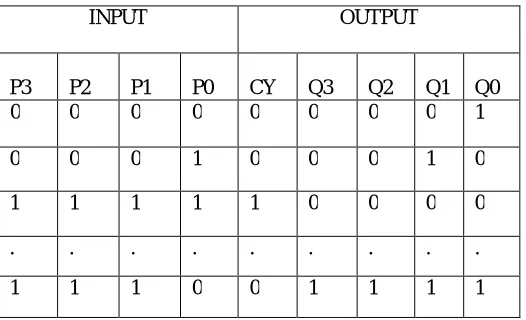
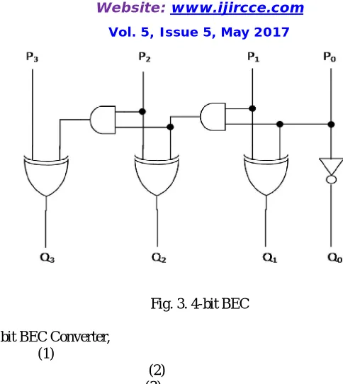
The area and power problem of regular SQRT CSLA was overcome by BEC [6] technique. The truth table of 4-bit BEC is given in Table 1. The Boolean expressions (1) to (5) are derived from the truth table. Figure 3 illustrates the structure of a 4-bit BEC. Numbers of logic sources are less in BEC thus reducing area and power consumption than that of regular SQRT CSLA. BEC is combination of NOT (~), AND (.), XOR (⊕) gates. P3, P2, P1, P0 are the inputs and Q3, Q2, Q1, Q0 are the outputs of BEC while CY is the final carry out.
Table 1: Truth Table of 4-Bit BEC
INPUT OUTPUT
P3 P2 P1 P0 CY Q3 Q2 Q1 Q0
0 0 0 0 0 0 0 0 1
0 0 0 1 0 0 0 1 0
1 1 1 1 1 0 0 0 0
. . . .
Fig. 3. 4-bit BEC
Boolean expression of 4 bit BEC Converter,
Q0 = ∼P0 (1)
Q1 = P1 ⊕P0 (2)
Q2 = P2 ⊕(P1 . P0) (3)
Q3 = P3 ⊕(P2 . P1 . P0) (4)
CY = P3 . P2 . P1 . P0 (5)
A. Architecture of SQRT CSLA Using BEC
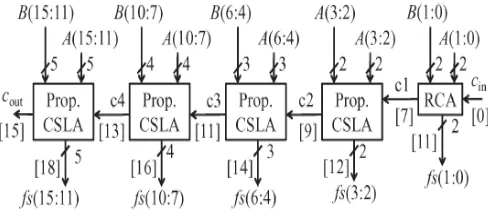
The architecture of 16-bit modified SQRT CSLA is shown in figure 4. The five groups consist of variable sized RCAs. CSLA consists of one RCA with Cin=0, BEC and mux. BEC logic is used instead of the RCA with Cin=1. A (n+1)-bit BEC is used to replace an n-bit RCA. In this design, the mux inputs are RCA (with Cin=0) output and BEC output. By comparing with regular 16 bit SQRT CSLA the area and power are reduced with a delay penalty.
Fig. 4: Modified 16 bit SQRT CSLA
B. Area calculation of SQRT CSLA using BEC
The group 3 of modified 16-bit SQRT CSLA using BECis elaborated in figure 5. The group3 has one 3-bit RCA and one 4-bit BEC instead of another RCA. The 3-bit RCA with Cin=0 consists of two FA and one HA whereas a 4-bit BEC Consists of three XOR gates, one NOT gate and two AND gates. Four 2:1 muxes are used to select the final sum and carry. The two inputs of mux are RCA with Cin=0 and BEC output. For group 3, 66 AOI gates are used as given below.
HA = 6 (1*6) XOR=15 (3*5) NOT=1 (1*1) AND=2 (2*1) MUX=16 (4*4) ……… Total Gate = 66
Fig. 5: Group3 of 16 bit Modified SQRT CSLA
IV.PROPOSEDADDERDESIGN
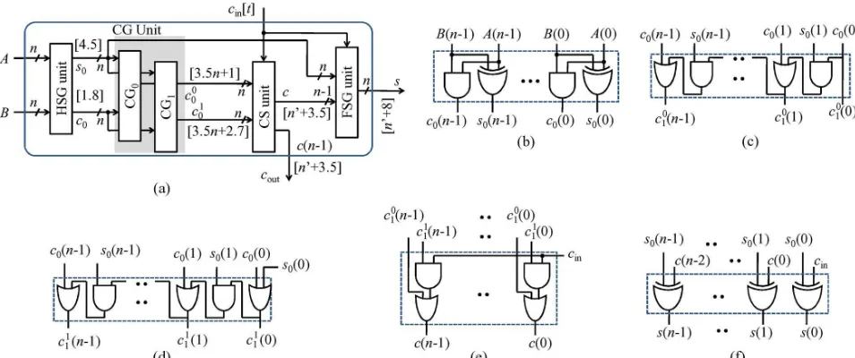
As shown in figure 7 the proposed CSLA consist of a 4 basic units, 1]one HSG(Half Sum Generator)unit, 2]one FSG(Full sum generator) unit, 3]CG(Carry Generator)unit, 4]one CS(Carry Select)unit. The CG unit consist of two CGs (CG0 and CG1). One is corresponding to carry input ‘1’ and another to carry input ‘0’.
A.
Architecture of Proposed CSLAThe architecture 16 bit proposed CSLA is as shown in figure 6. It is consist of one RCA and 4 proposed CSLA. The HSG receives two n-bit operands (A and B) and generate half-sum word s0 and half-carry word c0 of width n bits each. Both CG0 and CG1 receive s0 and c0 from the HSG unit and generate two n-bit full-carry words c01 and c11 corresponding to input-carry ‘0’ and ‘1’, respectively. The CS unit selects one final carry word from the two carry words available at its input line using the control signal cin. It selects c01 when cin = 0; otherwise, it selects c11.
B.
Area calculation of Proposed CSLAThe group of proposed n-bit SQRT CSLA is elaborated in figure 7. The n bit proposed SQRT CSLA has 4 basic units and each unit is consist of different sets of AND, OR and XOR gates. HSG unit is combination of AND and XOR gate.CG0 and CG1 units includes AND and OR gate combinations unit consist of AND and OR gate in series combination and FSG unit consist of XOR gate. For group 3 64 AOI gates are used as given below
HA=1 FA=1 AND=22 OR=12(3*4) XOR=28
……… Total Gate=64
Fig. 7: (a) Proposed CS adder design, where n is the input operand bit-width, and [∗] represents delay (in the unit of inverter delay), n = max (t, 3.5n + 2.7). (b) Gate-level design of the HSG. (c) Gate-level optimized design of (CG0) for
input-carry = 0. (d) Gate-level optimized design of (CG1) for input-carry = 1. (e) Gate-level design of the CS unit. (f) Gate-level design of the final-sum generation (FSG) unit.
V.TOOLSUSED
This work evaluates the performance of the proposed designs in terms of area, power by hand with logical effort and through Xilinx ISE 14.2(Verilog HDL).This coding is implemented in FPGA (Spartan 6).The Xilinx 14.2 (Verilog HDL) provide all simulation results. Area, Delay requirement of all type of carry select adders along with proposed carry select adder, so that it’s easy to compare and got conclusion that which system is good in all circumstances.
VI.SYNTHESISRESULTS
report and table 3. Shows CSA 16 bit proposed report which is run on Xilinx ISE 14.2(Verilog HDL)
Table 2: CSLA 16 Bit Exist ReportTable 3:CSLA 16 Bit Proposed Report
VII.SIMULATIONRESULTS
Simulation result for 16 bit regular CSLA and 16 bit proposed CSLA is as shown in figure 8 and figure 9 respectively. Waveforms for input, output and carry signal are generated.
VIII.EVALUATIONRESULTS
Table 4: Comparison of Regular and Modified Carry Select Adder
WORD SIZE
ADDER DELAY(ns) AREA(NO.OFLUTs)
16 bit
Regular CSLA
6.45 18
Modified CSLA
5.688 16
32 bit
Regular CSLA
10.73 39
Modified CSLA
8.859 32
As shown in Table 4, the proposed SQRT-CSLA involves significantly less area and less delay and consumes less power than the existing design which is run on Xilinx ISE 14.2 (Verilog HDL).This will implemented in Spartan 6 kit.
IX.CONCLUSIONANDFUTUREWORK
A simple approach is proposed in this paper to reduce the area and power of SQRT CSLA architecture. The reduced number of gates of this work offers the great advantage in the reduction of area and also the power. The modified CSLA architecture is therefore, low area, low power, simple and efficient for VLSI hardware implementation. I have analyzed the logic operations involved in the conventional and BEC-based CSLAs to study the data dependence and to identify redundant logic operations. I have eliminated all the redundant logic operations of the conventional CSLA and proposed a new logic formulation for the CSLA. In the proposed scheme, the CS operation is scheduled before the calculation of final-sum, which is different from the conventional approach. Carry words corresponding to input-carry ‘0’ and ‘1’ generated by the CSLA based on the proposed scheme follow a specific bit pattern, which is used for logic optimization of the CS unit. The proposed CSLA design involves significantly less area and delay than the recently proposed BEC-based CSLA. Due to the small carry-output delay, the proposed CSLA design is a good candidate for the SQRT adder. The ASIC synthesis result shows that the existing BEC-based SQRT-CSLA design involves 48% more ADP and consumes 50% more energy than the proposed SQRT-CSLA, on average, for different bit-widths.
REFERENCES
[1] K. K. Parhi, VLSI Digital Signal Processing. New York, NY, USA: Wiley, 1998.
[2]A. P. Chandrakasan, N. Verma, and D. C. Daly, “Ultralow-power electronics for biomedical applications,” Annu. Rev. Biomed. Eng., vol. 10, pp. 247– 274, Aug. 2008. [3] O. J. Bedrij, “Carry-select adder,” IRE Trans. Electron. Comput, vol. EC-11, no. 3, pp. 340–344, Jun. 1962.
[4]Y. Kim and L.-S. Kim, “64-bit carry-select adder with reduced area,” Electron. Lett., vol. 37, no. 10, pp. 614–615, May 2001.
[5] Y. He, C. H. Chang, and J. Gu, “An area-efficient 64-bit square root carry-select adder for low power application,” in Proc. IEEE Int. Symp. Circuits Syst., 2005, vol. 4, pp. 4082–4085.
[6]B. Ramkumar and H. M. Kittur, “Low-power and area-efficient carry-select adder,” IEEE Trans. Very Large Scale Integr. (VLSI) Syst., vol. 20, no. 2, pp. 371–375, Feb. 2012.
[7] I.-C. Wey, C.-C. Ho, Y.-S. Lin, and C. C. Peng, “An area-efficient carry select adder design by sharing the common Boolean logic term,” in Proc.IMECS, 2012, pp. 1– 4.