ABSTRACT
ZOHNI, OMAR SHARIFF. Design, Fabrication and Experimental
Characterization of PZT Membranes for Passive Low Frequency Vibration Sensing. (Under the direction of Dr. Gregory D. Buckner.)
Low frequency vibration sensing is being used increasingly to monitor the
health of machinery and civil structures, enabling “need-based” maintenance
scheduling and reduced operating costs. Passive sensors are of particular
interest because they don’t require input energy to monitor vibration. Modern
vibration sensors are often micro electromechanical systems (MEMS), and are
usually very basic in design consisting of a cantilevered beam with some type of
deflection sensing circuit. Under the influence of acceleration the beam deflects
from its nominal position and its deflection is measured using optical, capacitive
or piezoelectric techniques. MEMS sensors tend to exhibit very large stiffness to
mass ratios, making them best suited to high frequency vibration sensing.
Sensors utilizing the piezoelectric effect can achieve direct energy
conversion from the mechanical domain (strain) to the electrical domain (charge)
via piezoelectric coupling coefficients. To maximize the electrical output, lead
zirconate titanate (PZT) is an excellent piezoelectric material due to its high
coupling coefficients. However, the introduction of PZT into standard MEMS
processes is problematic because lead is considered a contaminant in most
delamination in thin film stacks have hindered the development of robust
fabrication processes for these devices.
This dissertation investigates candidate MEMS sensor geometries and
fabrication processes for passive low frequency vibration sensing. The addition of
silicon nitride (Si3N4) thin films into sol-gel deposited PZT stacks is studied, and
the effects of various adhesion layers on delamination and ferroelectric
characteristics are quantified. A fabrication process is developed allowing for
both front and back side contact for electrical measurements. The effects of thin
film stresses on the frequency response of PZT membranes are investigated
using experimental, analytical, and computational techniques. Results indicate
that thin film stresses in silicon dioxide (SiO2) and Si3N4 can shift the natural
frequencies of sensor membranes by as much as 20%. Optimization of sensor
membranes is conducted using available numerical methods, particularly finite
element analysis (FEA). Coupled electromechanical measurements of fabricated
membranes are conducted and experimental results are compared with
numerical and analytical solutions.
The research outlined in this dissertation represents the first known
investigation of passive MEMS vibration sensors specifically targeting such a low
frequency range. Also, the integration of PZT into a standard MEMS process
requiring low pressure chemical vapor deposition (LPCVD) Si3N4 has not been
which can be used for future work in this field. This process includes a reliable
adhesion layer which can be used when deep wet etching of silicon is required.
Recommendations for future work and for incorporating these results into
Design, Fabrication and Experimental Characterization of PZT Membranes for Passive Low Frequency Vibration Sensing
by
Omar Shariff Zohni
A dissertation submitted to the Graduate Faculty of North Carolina State University
in partial fulfillment of the requirements for the Degree of
Doctor of Philosophy
Mechanical Engineering
Raleigh, North Carolina
2009
APRROVED BY:
Dr. Richard Keltie Dr. Andre Mazzoleni
Dr. Richard Siergiej Dr. Yong Zhu
DEDICATION
My parents have been an integral part of my finishing this degree.
Through thick and thin they have loved and supported me. Words can’t describe
BIOGRAPHY
Omar Zohni was born and raised in Shamokin, Pennsylvania. He obtained a
Bachelor of Engineering degree from the University of Pittsburgh (Swanson
School of Engineering) in 1998, and a Masters of Science degree in Mechanical
Engineering from Johns Hopkins University (G.W.C. Whiting School of
Engineering) in 2002. His pursuit of the Doctor of Philosophy in Mechanical
ACKNOWLEDGEMENTS
I would like to thank,
• My advisor, Dr. Gregory D. Buckner, for being a great sounding board
and standing by me during this pursuit. I’ve learned a great deal from
him and he’s helped make this an extremely rewarding experience.
• The Department of Energy’s (DOE) Naval Nuclear Propulsion Program
(NNPP) for their generous fellowship and funding of my research.
• The team from Bechtel Bettis Inc in Pittsburgh for their support and
guidance during my summer practicums, especially Dr. Richard
Siergiej and Dr. Jeffery Maranchi.
• Committee members, Dr. Richard Keltie, Dr. Angus Kingon, Dr.
Richard Siergiej, Dr. Andre Mazzoleni, for their time and valuable
suggestions.
• The NCSU Nanofabrication Facility, specifically Joan O’Sullivan and
Dr. Ginger Yu for helping me get my devices fabricated.
• The Thin Film Dielectrics Group, specifically Taeyun Kim, Dr. Angus
Kingon and Dr. Jon-Paul Maria.
• Faculty and staff of the Department of Mechanical and Aerospace
Engineering, especially Mr. Rufus (Skip) Richardson and Mr. Mike
• Kimberly Wilk for keeping me at this when many times I felt like just
giving in, along with the rest of my friends and family for their support.
• Paul Drury for making sure I remembered that I didn’t have my PhD yet
TABLE OF CONTENTS
LIST OF TABLES...viii
LIST OF FIGURES ... ix
1. Introduction...1
1.1. Low Frequency Vibration Sensing ...1
1.2. Background ...4
1.3. Research Objectives...6
1.4. Organization of Dissertation ...8
2. Initial Design Concept Development...11
2.1. Candidate Geometries...12
2.1.1. Simple Beam Structures...12
2.1.2. Tethered Beam Structures ...18
2.1.3. Tethered Proof Mass ...24
2.1.4. Membrane Structures...29
3. Development of a Stacked PZT Fabrication Process ...33
3.1. PZT Stack Structure ...35
3.2. Adhesion Layer Study...39
3.2.1. Zr Adhesion Layer ...43
3.2.2. ZrO2 Adhesion Layer ...43
3.2.3. Ti Adhesion Layer...44
3.2.4. Ta Adhesion Layer ...44
3.3. Device Fabrication and Process Flow...45
4. Electrical and Physical Characterization of Stacked PZT Films...50
4.1. Adhesion Layer Electrical Results ...55
4.1.1. Zr Adhesion Layer ...55
4.1.2. ZrO2 Adhesion Layer ...55
4.1.3. Ti Adhesion Layer...56
4.1.4. Ta Adhesion Layer ...57
4.2. Discussion of Electrical Results...58
4.3. Film Quality and Microstructure ...59
5. Thin Film Stresses in PZT Stack Structures ...63
5.1. Thin Film Stress Measurements ...65
5.2. Dynamic Response of Membrane Structures ...76
5.3. Finite Element Analysis ...83
5.4. Conclusions ...89
6. Coupled Electro-Mechanical Testing ...90
6.1. Dynamic Response of Membrane Structures ...90
6.2. Finite Element Analysis ...96
7.1. Adhesion Layer Study...103
7.2. Thin Film Stress Study...104
7.3. Coupled Electro-Mechanical Measurements ...106
7.4. Conclusions ...108
8. Future Considerations ...110
8.1. Deep Reactive Ion Etching ...110
8.2. Cohesive Zone Modeling...113
8.3. Packaging Considerations...115
REFERENCES ...117
APPENDICIES...125
Appendix A: Reprint: O. Zohni, G. Buckner, T. Kim, A. Kingon, J. Maranchi, R. Siergiej, “Effect of adhesion layers on the ferroelectric properties of lead zirconium titanate thin films deposited on silicon nitride coated silicon substrates“, Thin Solid Films, vol. 516, pp. 6052-6057, 2008.
LIST OF TABLES
Table 2.1 – Solutions of characteristic beam equations for
β
nl
terms ...15Table 3.1 – Adhesion layers and processing conditions ...42
Table 4.1 - Comparison of relative dielectric constant and remnant polarization with adhesion layer thickness and PZT pyrolysis temperature ...59
Table 5.1 – Processing conditions for thin films...67
Table 5.2 – Wafer sample descriptions...70
Table 5.3 – Curvature and stress results for wafers A-D ...75
Table 5.4 – First natural frequency measurements for membranes with various dimensions...81
Table 5.5 – Material properties used in the ANSYS FEA model ...84
Table 5.6 – Comparison of measured results to FEA results (both stressed and unstressed) – 2.0 cm x 2.0 cm membrane...87
Table 6.1 – Mechanical material properties used in ANSYS FEA model ...95
Table 6.2 – First natural mechanical frequency measurements for membranes without proof mass with various dimensions...96
Table 6.3 – Piezoelectric material properties used in ANSYS FEA model...97
Table 6.4 – Intrinsic stress values...98
Table 6.5 – Comparison of measured results to FEA results (both stressed and unstressed) –2.0cm x2.0cmmembrane...100
LIST OF FIGURES
Figure 2.1 – Simple beam structures: (a) Fixed-free (cantilever), (b) fixed-fixed.12 Figure 2.2 – Dependence of first natural frequency on beam length and
thickness: cantilevered beam...16 Figure 2.3 – Dependence of first natural frequency on beam length and
thickness: fixed-fixed beam...17 Figure 2.4 – Tethered beam structure with N lateral segments ...19 Figure 2.5 – First natural frequency dependence on geometry for an n-segment serpentine structure
(
t
=
10
µ
m
)
...21 Figure 2.6 – FEA modal analysis results for a serpentine beam:t
=
25
µ
m
,1000
µ
=
l
m
,n
=
3
...22Figure 2.7 – Comparison of analytical (Equation 2.8) to computational (FEA) natural frequency results for
t
=
25
µ
m
,l
=
1000
µ
m
...23 Figure 2.8 – Tethered proof mass structure...25 Figure 2.9 – Quarter-symmetric model used for FEA of tethered beam structure with proof mass...27 Figure 2.10 – Comparison of analytical equation to FEA results for variouslengths and number of turns ...28 Figure 2.11 – Square membrane sensing structure (
t
=
10
µ
m
,l
m=
5
cm
) ...29 Figure 2.12 – Square membrane structure with proof mass (t
=
10
µ
m
,5
=
ml
cm
) ...30 Figure 2.13 – FEA modal analysis results from membranes without proof mass with various thickness and length values (t
=
50, 100, 250, 500
µ
m
,1, 2, 4
=
mFigure 4.3 – Typical XRD result for PZT Material [58]...54
Figure 4.4 – Typical SEM result for a BaTiO3 material [59]...55
Figure 4.5 – εr-V and polarization for 25 nm oxidized Zr adhesion layer...56
Figure 4.6 – εr-V and polarization curves for 15 nm Ti adhesion layer...57
Figure 4.7 – εr-V and polarization curves for 15 nm Ta adhesion layer...58
Figure 4.8 – SEM cross section of PZT using 25 nm Ta adhesion layer...60
Figure 4.9 – X-Ray diffraction data for PZT deposited with Ta adhesion layer ...61
Figure 5.1 – Toho FLX-2320-S stress measurement system...66
Figure 5.2 – Initial curvature profiles for 4 SSP bare silicon wafers (A-D)...70
Figure 5.3 – Absolute curvature profiles after film deposition wafers (A-D) ...72
Figure 5.4 – Thin film stresses in Si3N4 (A), SiO2 (B-C) and SiO2:Si3N4 stacks (D) ...73
Figure 5.5 - Process description for creation of silicon membranes in the PZT stack. (a) Bare silicon wafer, (b) thermal oxidation (3000Å of SiO2), (c) LPCVD (1000 Å of Si3N4), (d) spin-on patterning and exposure of photoresist (e) RIE to expose silicon and (f) KOH wet etch to create a membrane ...77
Figure 5.6 – Customized sensor platform with optical displacement sensor and micropositioners attached ...78
Figure 5.7 – Experimental impulse response from optical sensor – 2.0cm×2.0cm membrane with a thickness of 25µm. ...79
Figure 5.8 – Experimental impulse response from optical sensor – 2.0cm×2.0cm membrane with a thickness of 110µm...80
Figure 5.9 – Fast Fourier Transform – 2.0cm×2.0cm membrane with a thickness of 110µm...81
Figure 5.10 – Measured response for membranes with various dimensions ...82
Figure 5.11 – FEA boundary conditions for ¼ symmetric model...84
Figure 5.12 – FEA model of membrane structure – (a) complete mesh, (b) close up of mesh showing Si/SiO2/Si3N4 stack...85
Figure 5.13 – FEA natural frequency normalized modal displacement for a 2.0cm×2.0cm membrane with a thickness of 50µm – unstressed film ...86
Figure 5.14 – A comparison of measured, closed form and stressed FEA results to unstressed FEA results – 2.0cm×2.0cm membranes ...88
Figure 6.1 – Sensor platform for electromechanical testing ...91
Figure 6.2 – Electrical impulse response from microprobes for a 2.0cm x2.0cm x10µm membrane ...93
Figure 6.3 – FFT of electrical impulse response from microprobes for a 2.0cm x2.0cm x10µmmembrane ...93
Figure 6.5 – FFT of mechanical impulse response for a
2.0cm x2.0cm x10µmmembrane ...94
Figure 6.6 – FEA model of membrane structure – (a) complete model, (b) close up of model showing full PZT stack ...97 Figure 6.7 – FEA natural frequency normalized modal displacement response
2.0cm x2.0cm x100µm– unstressed films ...99
Figure 6.8 – FEA design optimization results for proof mass-enhanced
membrane 2.0cm x2.0cm x10 µm ...101
Figure 8.1: DRIE process description for fabricating proof mass enhanced silicon membranes in a PZT stack. ...112 Figure 8.2: DRIE process stages: (a) SF6 plasma etch, (b) C4F8 plasma deposits
1. Introduction
1.1.
Low Frequency Vibration Sensing
Low frequency vibration sensing is the process of measuring the response of
a mechanical component to an external stimulus; it is being used increasingly to
monitor the health of machinery and civil structures, enabling “need-based”
maintenance scheduling and reduced operating costs. Modern vibration sensors
are designed to measure one of three states of mechanical vibration:
displacement, velocity, and acceleration. Displacement sensors, both contacting
(linear variable differential transformers, linear potentiometers, etc.) and
non-contacting (optical displacement sensors, inductive sensors, etc.), tend to be
bulky, expensive and require that the moving mechanical component be in close
proximity to a fixed sensing component. This proximity requirement limits the
measurement resolution and the amplitude of vibration that can be detected.
Velocity sensors (velometers) typically rely on electromagnetic induction (back
emf) to produce a speed-dependent voltage signal. Because such devices
frequently incorporate permanent magnets, copper windings, and back iron they
also tend to be bulky and costly. For these reasons, acceleration sensors
(accelerometers) are the preferred method for general vibration sensing.
Acceleration signals can be integrated to obtain velocity and displacement
information, though issues with noise and sensor drift must be taken into
consideration [1].
Low frequency piezoelectric accelerometers are common vibration sensors
for machinery monitoring, biomedical applications, material evaluation and modal
testing [2, 3]. Although piezoelectric accelerometers come in a large variety of
configurations (compression mode, shear mode, flexural mode, etc.), most
contain a quartz or piezoceramic sensing element in contact with a proof mass.
As the proof mass accelerates, it exerts a force on the sensing element.
Piezoelectric coupling coefficients in the sensing element convert the mechanical
strain into an electric charge that is proportional to the acceleration. This charge
is amplified (internally or externally) to produce a voltage signal proportional to
acceleration. The ceramic material properties can be tailored to allow for design
flexibility by optimizing the coupling coefficients as well as the desired frequency
range. Single and multi-axis accelerometers are available to detect both the
magnitudes and directions of acceleration for an increasing number of industrial
and domestic applications. Their hermetically sealed construction allows for
usage in harsh environments and at elevated temperatures [4].
Historically, low frequency vibration sensing (<300 Hz) required macro scale
components (large proof masses and sensing elements) and associated
electro-mechanical systems (MEMS), and are usually very basic in design consisting of
a cantilevered beam with some type of deflection sensing circuit. Under the
influence of acceleration the beam deflects from its nominal position and the
deflection is measured using optical, capacitive or piezoelectric techniques.
MEMS represent the integration of micromechanical and electrical components
with actuation and sensing elements onto a common substrate using
microfabrication technology. The electronics are fabricated using Integrated
Circuit (IC) processing sequences such as Complementary
Metal-Oxide-Semiconductor (CMOS) or Bipolar CMOS (BiCMOS) processes. The
micromechanical components are fabricated using compatible "micromachining"
processes that selectively etch away portions of the silicon wafer or add new
structural layers. The actuation and sensing elements couple the mechanical
and electrical components and convert energy between the two domains. MEMS
sensors, for example, might employ the direct piezoelectric effect to convert
mechanical energy to electrical energy. MEMS actuators might employ the
converse piezoelectric effect to achieve the converse energy transfer.
Recent advances in MEMS technology have resulted in the commercialization
of sensors to measure acceleration and inclination on civil structures, industrial
machines and vehicles. MEMS accelerometers tend to exhibit very large
deployment systems for modern automobiles, where the device monitors
changes in acceleration to determine when a collision occurs [5]. MEMS
accelerometers have been integrated alongside gyroscopes for inertial guidance
systems and instrument positioning systems [6].
MEMS-based accelerometers have undergone a large market increase
recently, as they are being incorporated into many personal electronic devices
[7]. Smartphones, personal digital assistants and cameras are utilizing this
technology to handle for example, switching between landscape and portrait
modes as devices are turned on their sides. Laptops are using MEMS based
accelerometers to detect shock type events, protecting against hard disk crashes
in the event an unexpected drop. It is estimated that more than 10 billion MEMS
chips will be integrated into mobile phones by 2010 [7] and that the global MEMS
market will exceed $20 billion by 2016 [8].
1.2.
Background
Piezoelectric materials, specifically lead zirconium titanate (PZT), are
attractive for MEMS-based sensing applications because of their high sensitivity
and low noise characteristics [9, 10]. PZT thin films have well-documented
pyroelectric, piezoelectric and ferroelectric properties [11]. Various methods of
frequency (RF) co-sputtering [13], metallorganic chemical vapor deposition
(MOCVD) [14], pulsed laser deposition (PLD), and sol–gel techniques [15-17].
The literature is replete with research involving the design and fabrication of
MEMS vibration sensors, including capacitive silicon micromachined vibration
sensors with seismic masses [18], sensors for harsh environments [4],
geophysical sensors [19], and conductive ball sensors [20]. Recently there have
been efforts to develop reliable PZT processes that can be used to create
piezoelectric transducer elements [21]. The introduction of PZT into the MEMS
fabrication process is difficult because PZT is not a CMOS-compatible material,
and all wafer handling must take place in dedicated areas. Other piezoelectric
materials, such as Aluminum Nitride (AlN), are CMOS-compatible and can be
used to overcome these limitations. However, these materials have limited
coupling coefficients between the electrical and mechanical domains, particularly
for bending-induced strains.
Current macro based low frequency vibrations sensors tend to be bulky,
difficult to use in confined spaces, or outfitted on a mechanical component. The
desire to miniaturize low frequency vibration sensors is driven by reducing weight
and limited space requirements in mechanical equipment. These requirements
push current research into the micro and nano scale for vibration sensing. The
This research presents the first attempt to achieve this type of active vibration
sensing, utilizing a passive approach and bulk silicon etching processes.
1.3.
Research Objectives
This thesis presents a methodology for designing and fabricating passive PZT
based MEMS accelerometers to sense relatively low frequency signals (50 – 500
Hz), a design objective not previously reported in the literature. The passive
nature of the vibration sensor makes it necessary for it to operate near the top of
its linear range, which is normally up to 20% of resonance. While many current
sensors can be used to monitor these low frequency vibrations, their amplitude
would be too small to achieve enough of a response without some amplification.
Such low frequency sensors could be used to monitor deterioration and fatigue
associated with civil structures and mechanical equipment by detecting shifts in
their fundamental frequencies, indicative of changes in stiffness often caused by
cracks or larger failures [22]. Various sensor geometries were investigated
including basic beam structures, tethered or serpentined beams, serpentined
beams with a proof mass, and membrane structures. Using both closed form
analytical solutions as well as finite element analysis (FEA) these designs were
investigated and evaluated for feasibility.
The sensor utilizes the piezoelectric effect, specifically by incorporating PZT
ensure appropriate bandwidth. FEA is also used to confirm the piezoelectric
coupling coefficients and to characterize the effects of intrinsic thin film stresses
on the dynamic response.
Mechanical, electrical and coupled electro-mechanical dynamic responses
are measured for these structures. The mechanical response is measured using
an optical displacement sensing technique. The MEMS sensor is excited using
an external impulse and the displacement response is measured. The electrical
response is measured via electrical probes that make contact with the top and
bottom electrodes which sandwich the piezoelectric element embedded in the
vibration sensor. The probes measure the accumulated charge after the
vibration sensor is excited.
The research outlined in this dissertation represents the first known
investigation of passive MEMS vibration sensors operating in this frequency
range. Also, the integration of PZT into a standard MEMS process with deep wet
chemical silicon etching requiring LPCVD Si3N4 has not been reported
previously. A robust integrated PZT process is also developed which can be
used for future work in this field. This approach includes a reliable adhesion
layer which can be used when deep wet etching of silicon is required. An
alternative approach using Deep Reactive Ion Etching (DRIE) techniques to
Si3N4 layers for masking. Both of these approaches are viable techniques for
creating deep trenches in silicon. The wet etching technique is one that can be
used in nearly any fabrication facility, while the DRIE approach is limited because
it is a relatively new technique and DRIE equipment is expensive and not
currently available in all fabrication facilities.
1.4.
Organization of Dissertation
This dissertation is structured as follows:
Chapter 2 – Initial Design Concept Development. This chapter introduces
various candidate geometries for vibration sensing. Utilizing both MathCAD©
and ANSYS© these geometries allow for an exploration of the design space with
the goal of achieving low frequency vibration.
Chapter 3 – Development of Stacked PZT Fabrication Process. Existing
work utilizing PZT in MEMS fabrication has been performed using a standard
process; this work deviates from that process and requires a new fabrication
technique. Various adhesion layers are tested with their results reported within.
An initial complete fabrication process is also developed allowing for both front
and back side contact to measure the electrical response.
Chapter 4 – Electrical and Physical Characterization of Stacked PZT Films.
The electrical characteristics, Polarization and Relative Dielectric Constant vs.
verifies that the desired hysteresis behavior is occurring. Scanning Electron
Microscopy (SEM) and X-Ray Diffraction (XRD) techniques are also utilized to
verify the orientation and presence of the desired crystalline structure of PZT.
Chapter 5 – Mechanical Membrane Testing. This chapter discusses the
mechanical testing of membrane sensors. The response is measured using
optical sensing techniques and compared with both closed form and FEA.
Because Low Pressure Chemical Vapor Deposition (LPCVD) Silicon Nitride
(Si3N4) becomes a part of the enhanced stack, thin film stress measurements are
also investigated and their effect on the vibration characteristics reported.
Chapter 6 – Coupled Electro-Mechanical Testing. This chapter reports the
coupled electro-mechanical testing for the membrane structures. Coupled
testing allows for the verification of induced charges as a result of mechanical
vibration. Responses in the desired frequency range are measured with both
electrical probe measurements of charge and optical mechanical measurements
of vibration. FEA is also used to calculate the measured charge using typical
material properties for the elements in the sensor. These calculations are
compared to device measurements.
Chapter 7 – Summary and Conclusions. This chapter summarizes the
research and its findings. Highlighted are the discovery of an adhesion layer for
stresses on vibration response, and the coupled electro-mechanical
measurements that show the device responding as expected.
Chapter 8 – Future Considerations. This chapter identifies additional
experiments that can be used to further this research. The utilization of Deep
Reactive Ion Etching (DRIE) would significantly speed up the process and
simplify device fabrication. Cohesive zone modeling in ANSYS© would allow for
a better understanding of the delamination that was observed in various
2. Initial Design Concept Development
Macro-scale fabrication techniques, such as milling, turning, forging and
casting allow for the creation of complicated 3D geometries in a variety of
materials. MEMS fabrication, however, relies extensively on photolithographic
deposition and wet/dry etching processes for silicon substrates that limit the level
of complexity that can be achieved. MEMS devices are almost always simple
planar or conformal structures with relatively basic geometries and limited
material options [23].
MEMS designs are also limited by the physics of their scale: because their
surface to volume ratios are large, surface effects like electrostatics and wetting
frequently dominate the inertial effects required for vibration sensing.
Furthermore, the cantilevered sensing elements commonly used in MEMS
accelerometers have very high stiffness to mass ratios, pushing the sensing
range for MEMS devices into the MHz and GHz frequencies [24].
While the desire to build complex sensor structures to achieve the design
requirements is compelling, the inherent design limitations of MEMS devices limit
the creativity that can be used. Unlike macro-scale fabrication processes, where
imagination frequently dictates the design process, micro-scale fabrication
processes are presently limited to planar structures. These fabrication
sensing, lead to the consideration of relatively basic structures in the following
sections.
2.1.
Candidate Geometries
2.1.1. Simple Beam Structures
The first sensor designs considered were simple beam structures, both
fixed-free (cantilevered) and fixed-fixed beams, shown in Figure 2.1. This preliminary
analysis relied on the following classical Bernoulli-Euler beam assumptions [25]:
• Uniform, slender beams without axial loads
• Linear, homogenous, isotropic elastic materials
• Plane sections remain planar
• Beam’s plane of symmetry is also the plane of vibration so that
rotation and translation are decoupled
• Rotary inertia and shear deformation can be neglected
(a) (b)
The validity of some of these assumptions is questionable; for example it is
well known that silicon is an anisotropic material. However, for the purpose of
initial design concept evaluation these assumptions can be used and then
revisited for validity by comparing analytical predictions to FEA simulations and
experimental data.
By applying appropriate boundary conditions and summing moments and
forces, these two beam structures can be reduced to their characteristic
equations [25]:
1 cosh(
+
β
l
) cos(
β
l
)
=
0
(2.1)1 cosh(
−
β
l
) cos(
β
l
)
=
0
(2.2)Where:
•
l
=
Length of beam
(
µ
m
)
•
(
)
2
4
ρ ω
4β
µ
−=
A
m
EI
•
density of beam
2.3 10
15kg
3for silicon
m
ρ
µ
−
=
=
⋅
•
A
=
cross sectional area
=
bt
(
µ
m
2)
•
b
=
width of beam
(
µ
m
)
•
natural frequency
rad
s
ω
=
•
E
=
Young's Modulus 1.90 10
=
⋅
5MPa
for silicon
These equations can be used to find the beam’s th
n
natural frequencyf
n as afunction of the design parameters and material properties:
4 2
4 2
(
)
1
(
)
2
4 3
n n
n
l EI
t
l
E
f
Al
l
β
β
ρ
π
π
ρ
=
⋅
=
(2.3)•
3
Area Moment of Inertia
for rectangular cross section
12
=
=
bt
I
Note that Equation 2.3 is applicable to both beam configurations; in fact it can
be used for any combination of boundary conditions (free, simply supported or
fixed) subject to the Bernoulli-Euler beam assumptions stated previously. Only
the characteristic equations (i.e., Equations 2.1 and 2.2) are dependent on the
specific BC’s. Table 2.1 presents
β
nl
solutions for the cantilevered andTable 2.1 – Solutions of characteristic beam equations for
β
nl
termsn
Cantilever Beamn
l
β
Fixed-Fixed Beam
n
l
β
1 1.875 4.730
2 4.694 7.853
3 7.855 10.996
4 10.996 14.137
5 14.137 17.279
5
n
>
2(
1)
2
n
−
π
2(
1)
2
n
+
π
An interesting observation can be made from Equation 2.3: the beam’s
natural frequencies are not dependent on beam width
b
. This results from acancellation of
b
inI A
(both the areaA
and moment of inertiaI
are directlyproportional to
b
. For this reason, the design parameter with the greatest effecton natural frequency is beam length
l
, which has an inverse square relationshipwith frequency. Beam thickness
t
is linearly related to natural frequency, whilethe ratio of material properties
E
ρ
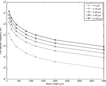
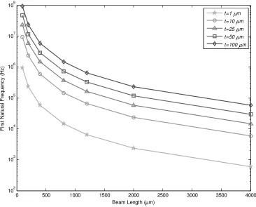
has the smallest effect. Figures 2.2 and 2.3illustrate the dependence of first natural frequency on beam length and thickness
0 500 1000 1500 2000 2500 3000 3500 4000 101 102 103 104 105 106 107 108
Beam Length (µm)
F irs t N at ur al F re qu en cy ( H z)
t=1 µm t=10 µm t=25 µm t=50 µm
t=100 µm
0 500 1000 1500 2000 2500 3000 3500 4000 102 103 104 105 106 107 108
Beam Length (µm)
F irs t N at ur al F re qu en cy ( H z)
t=1 µm t=10 µm t=25 µm t=50 µm t=100 µm
Figure 2.3 – Dependence of first natural frequency on beam length and thickness: fixed-fixed beam
These figures reveal that even extremely long and thin beams (
l
=
4000
µ
m
,1
t
=
µ
m
) do not exhibit first natural frequencies in the range of interest (50-300Hz). Furthermore, such feature thicknesses are not practical using standard wet
etching techniques for silicon. With KOH etching, for example, a practical
Another complication with simple beam structures is secondary bending
modes. Although beam width
b
has little effect on the first natural frequency ofthese beams, as it becomes closer in magnitude to beam thickness
t
the secondnatural frequency approaches the first. For example, when beam thickness
t
isequal to beam width
b
, both the vertical and lateral bending modes have exactlythe same natural frequency. This problem can be avoided by ensuring there is
enough difference between these two design parameters. Another problem that
is more difficult to avoid is the excitation of torsional modes that cause the beam
to twist about its neutral axis. As the
l t
ratio increases, the first torsionalfrequency approaches the first bending frequency of the structure. These
complications eliminated the cantilevered and fixed-fixed beam designs from
further consideration.
2.1.2. Tethered Beam Structures
As stated in Section 2.1.1, the design parameter with the greatest effect on
the first natural frequency of simple beams is beam length. One option for
increasing the effective beam length while maintaining compactness is the
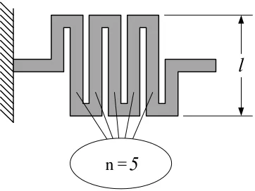
l
N=5
Figure 2.4 – Tethered beam structure with N lateral segments
Approximate solutions for natural frequency of the serpentine beam can be
derived by applying the Bernoulli-Euler beam assumptions to each segment of
the beam structure. The straight lateral sections can be modeled as springs in
series that oppose the motion perpendicular to the plane of Figure 2.4. Each
long section
l
k
and the two short sections2
l
k
contribute to the total equivalentstiffness
t
k
:2
1
2
t l l
n
k
=
k
+
k
or2 2
2
=
+
l l t l lk k
k
nk
k
(2.4)Where, from beam theory [25]:
3 3 3 3 3 12 4 Ewt Ewt k l l l
= = and
(
)
3 3
3 2
2 3 3
12 2 Ewt Ewt k l l l
= = (2.5)
Substituting (2.5) into (2.4) yields an expression for the equivalent stiffness of a
serpentine structure:
(
)
3 3 4 1 = + Ewt k t l n (2.6)
A similar modeling exercise provides expressions for the equivalent mass of the
serpentine structure:
0.23
ρ
(
1)
=
+
eq
m
wt n
l
(2.7)Equations 2.6 and 2.7 can be used to find the first natural frequency of an n
-segment serpentine structure:
(
)
3
3
4
1
1
1
2
π
2
π
0.23
ρ
(
1)
+
=
=
+
t eqEwt
k
l
n
f
m
wt n
l
2
1.0425
(
1)(4
1)
Recalling that
10
µ
m
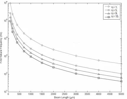
is the practical minimum layer thickness for KOH wetetching processes, Figure 2.5 illustrates the dependence of natural frequency on
the number of lateral segments (
n
) and beam length (l
) for a beam thickness of10
t
=
µ
m
.These analytical results were compared to an FEA model that underwent a
mesh convergence study to ensure accuracy. Parabolic brick elements with
mid-side nodes (20-noded) were used to model the beams with a minimum of two
elements each in the thickness and width directions to ensure numerical
accuracy. Each element node featured three degrees of freedom (DOF),
representing deflections in each orthogonal direction. Fixed boundary conditions
were applied at the base of each structure, thus constraining those nodes from
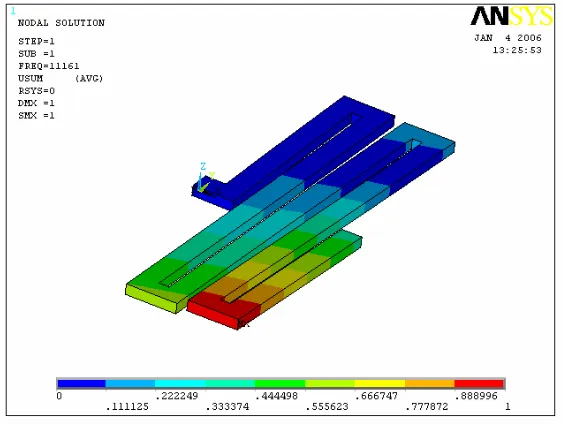
any movement. Figure 2.6 shows an FEA modal analysis contour plot, which
predicts a first natural frequency of
11,161
Hz
for a serpentine structure with25
µ
=
t
m
,l
=
1000
µ
m
andn
=
3
.Figure 2.6 – FEA modal analysis results for a serpentine beam:
t
=
25
µ
m
,1000
µ
=
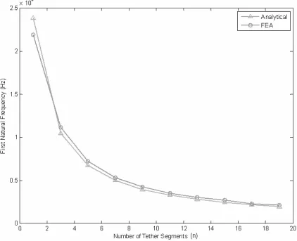
Figure 2.7 compares FEA results to the analytical results of Figure 2.5 for a
serpentine structure with
t
=
25
µ
m
,l
=
1000
µ
m
and a variable number oftethers.
Figure 2.7 – Comparison of analytical (Equation 2.8) to computational (FEA) natural frequency results for
t
=
25
µ
m
,l
=
1000
µ
m
assumptions of Bernoulli-Euler beam theory, most notably approximations
regarding mass participation in the vibration process.
Although the serpentine beam approach successfully lowered the natural
frequencies for a given package length, the resonant frequencies are still much
higher than the design requirements dictate. Furthermore, FEA revealed that
torsional modes in the desired sensing range were excited. To combat this
effect, tethered devices with proof masses were investigated next.
2.1.3. Tethered Proof Mass
To reduce the effects of secondary and torsional bending modes, another
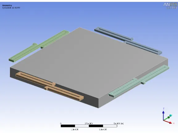
design incorporating four serpentine tethers was considered, Figure 2.8. This
configuration allows for the addition of a proof mass to further lower the
Figure 2.8 – Tethered proof mass structure
The overall stiffness of this device can be approximated as four (4) individual
tethers connected in parallel:
(
)
3 3
4
4
4
1
eq t
Ewt
k
k
l
n
=
=
+
(2.9)Because the square proof mass dominates the inertial effects, the equivalent
mass can be approximated based solely on its contribution:
2
ρ
=
eq m m
m
l t
(2.10)3 3 2
1
1
2
(4
1)
t
eq m m
k
wt
E
f
m
l l t
n
π
π
ρ
=
=
+
(2.11)Where:
•
l
m=
side length of proof mass
•
t
m=
thickness of proof mass
Once again, FEA simulations were compared to these analytical results.
Figure 2.9 shows the model used for analysis. Because the device exhibits
fourfold symmetry, the FEA model was simplified (and computation times
reduced) by modeling one fourth of the structure without sacrificing accuracy.
Appropriate boundary conditions were applied along the planes of symmetry to
constrain rotation and lateral motion. The structure was also fixed at the outer
face of the tethered structure and modal analysis was conducted. The following
geometric parameters were used for the baseline comparison of the closed form
solution and the FEA model:
•
Thickness of proof mass
=
500
µ
m
•
Side of proof mass
=
Length of beam
•
Width of beams
=
30
µ
m
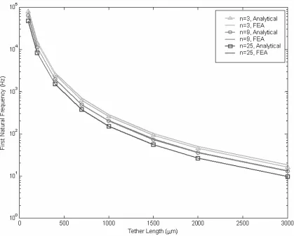
Figure 2.10 compares analytical to FEA results for tethered proof mass
structures with various numbers and lengths of tether segments.
Figure 2.10 – Comparison of analytical equation to FEA results for various lengths and number of turns
Clearly, these enhanced tethered devices have natural frequencies in the
range of interest (<300 Hz), but they are more challenging to fabricate as they
require backside alignment to ensure the tethers are aligned with the membrane
sides (since the membranes will be etched away first). This hardware is not
available at NCSU facilities. Furthermore, the relative differences in size, mass
and make it difficult to ensure that they have fully released after etching. For
these reasons, fabrication of tethered mass structures was not pursued, but
simpler membrane structures were considered.
2.1.4. Membrane Structures
The final sensor topologies investigated were square membrane structures,
with and without proof mass enhancement. Figures 2.11 and 2.12 show FEA
models of both membrane structures.
Figure 2.12 – Square membrane structure with proof mass (
t
=
10
µ
m
,5
=
m
l
cm
)An analytical expression for the fundamental frequency of a square
membrane structure is [27]:
2 2
9
(1
)
3
mt
E
f
l
ρ
υ
π
=
+
(2.12)Where:
•
t
=
membrane thickness
(
µ
m
)
•
l
m=
side length of membrane
(
µ
m
)
•
E
=
Young's Modulus 1.90 10
=
⋅
5MPa
for silicon
•
density of beam
2.3 10
15kg
3for silicon
m
ρ
µ
−
•
υ
=
Poisson's ratio = 0.24 for silicon
As with the simple beam structures, the membrane’s fundamental frequencies
vary linearly with membrane thickness and with the inverse square of side length.
Finite element analysis was compared to Equation 2.12 to explore the design
space for these devices. As with the previous designs, these FEA models were
constructed using 20-noded solid brick elements, and constrained in all directions
at the base of the four tethers. Modal analysis results are shown in Figure 2.13
for membranes of various thicknesses and side lengths. As expected from
Equation 2.12, there is a linear variation in frequency with respect to thickness
1 1.5 2 2.5 3 3.5 4 101 102 103 104 105
Membrane Length (cm)
F irs t N at ur al F re qu en cy ( H z)
t=50µm t=100µm t=250µm t=500µm
Figure 2.13 – FEA modal analysis results from membranes without proof mass with various thickness and length values (
t
=
50, 100, 250, 500
µ
m
,1, 2, 4
=
m
l
cm
)The analytical and computational results presented in this chapter, coupled
with fabrication considerations and the availability of resources at NCSU, dictated
the selection of proof mass enhanced membrane structures for low-frequency
MEMS acceleration sensing. Although the natural frequency results for the
tethered proof mass concepts were as good as (if not better than) the membrane
structures, these designs were not pursued for the reasons discussed above.
The next chapter discusses fabrication processes that can be used to fabricate
3. Development of a Stacked PZT Fabrication Process
Lead zirconium titanate (PZT) materials are of particular interest because of
their pyroelectric, piezoelectric and ferroelectric properties. PZT-based MEMS
technology is attractive for sensing applications because of its high sensitivity
and low noise characteristics [9, 10]. Various methods of attaining PZT thin films
are available, including hydrothermal powders [12], radio frequency (RF)
co-sputtering [13], metallorganic chemical vapor deposition (MOCVD) [14], pulsed
laser deposition (PLD) [28], and sol–gel techniques [15-17]. Of these available
methods, sol-gel processing is used widely in the MEMS community because of
its ability to create films with high d33 electromechanical coupling coefficients
[29-33]. This compensates for many of its associated complexities, most notably its
requirement for high processing temperatures.
RF co-sputtering is a deposition technique that is gaining traction because of
its relative ease of operation. In addition, the bottom electrode and PZT layers
can be deposited without moving the sample [13]. The downside of this
approach is the introduction of lead into the fabrication facility, specifically into
the sputtering system. Lead is considered a contaminant in silicon fabrication
facilities, thus this technique requires a dedicated sputtering system or a
MOCVD is a more complicated deposition process as it requires a cold-walled
deposition chamber integrated with a liquid delivery system, a showerhead, a
heater and a specifically designed vaporizer [12]. This deposition technique also
tends to yield high surface roughness, causing degradation in the quality of the
PZT film [34].
PLD is popular because it easily allows for the reproduction of the chemical
makeup of PZT thin films, which means the coupling coefficients and electrical
characteristics are well known and easily repeatable [35]. However, it creates
similar concerns as co-sputtering in that it contaminates the fabrication facility,
and can also require the development of the ceramic target using a solid state
reaction technique in which a conventional sintering process can be used. This
is difficult because these types of processes are generally not available in
conventional fabrication facilities. [13].
This chapter focuses on the fabrication of PZT MEMS devices using sol–gel
precursors and spin-on thin film processing techniques. These approaches were
selected in part because of the collective research expertise and extensive
facilities available at NCSU’s Electroceramic Thin Films Laboratory. During the
course of this work at the NCSU facilities, samples containing PZT were not
processed in high temperature oxidation and other systems used by silicon
3.1.
PZT Stack Structure
The majority of sol–gel PZT thin film research has been conducted using a
standard stack structure [15-17, 29-33], with only small variations in processing
conditions or thicknesses of individual layers [36, 37]. The stack consists of a
silicon (Si 100) wafer with a thermal SiO2 layer grown on the front and back
sides. Generally, this silicon dioxide layer is 600 nm thick, but depending on the
fabrication specifications this thickness can be modified, which can be beneficial
if it is being used as a structural layer. The SiO2 layer promotes adhesion of the
bottom electrode layers and serves as an insulator between the device and the
substrate. Next a thin titanium (Ti) adhesion layer (15 nm) is RF sputtered on the
front side of the wafer, followed by a thin platinum (Pt) layer (100 nm) which is
also RF sputtered onto the front side. The titanium (Ti) adhesion layer is chosen
over other materials because of its robustness in adhering the platinum to the
oxide layers [38, 39].
Next, a PZT precursor is spun onto the wafer. This solution is prepared using
an organometallic mixture of lead acetate (Pb(CH3COO)2), zirconium acetate
(ZrO(CH3COO)2), tetrabutyl titanate (Ti(OC4H9)4) and a methanol (CH4O) solvent.
The Pb (ZrxTi1 −x)O3 precursor can vary in concentration from x=30–70% [38].
Typically, the spin-on is done at 2500 rpm for 30 s, followed by drying on a hot
final pyrolysis step is required to crystallize the PZT material. This is done by
placing the sample in an open air furnace at 500–700°C. Finally, the sample is
placed back into an RF sputtering system and a top platinum or aluminum
electrode is deposited. A more detailed description of the process can be found
in [40].
A problem with this standard process arises when membrane structures need
to be fabricated via backside wet etching into the silicon. Standard backside wet
etching in potassium hydroxide (KOH) of Si is incompatible with the underlying
SiO2 layer. For bulk wet micromachining in KOH, a layer of Low Pressure
Chemical Vapor Deposition (LPCVD) silicon nitride (Si3N4) is needed as a
masking layer on the backside of the silicon. Silicon dioxide cannot be used as a
masking agent as it has an etch rate of nearly 1 µm/hour, while the LPCVD
silicon nitride has an etch rate of < 1 nm/hr. An alternative etchant for silicon is
Ethylene Diamene Pyrocatecol (EDP), which has the advantages of fast etch
rates, good selectivity, and high <100> to <111> plane etch ratios.
Unfortunately, EDP is also extremely corrosive, highly carcinogenic, and is easily
inhaled or absorbed through the skin. Consequently, EPD is not available in the
NC State fabrication facility and was not used for this research. Because LPCVD
silicon nitride is deposited on both the front and back sides of the wafer, it
becomes an integral part of the PZT stack and creates adhesion concerns.
lead to fragile or buckled membrane structures [41]. Plasma Enhanced Chemical
Vapor Deposition (PECVD) silicon nitride films, deposited at much lower
temperatures and applied on the backside of the wafer, are not effective masks
for KOH etching [10]. The density of PECVD silicon nitride is much lower than
LPCVD, and due to the presence of pinholes, the PECVD silicon nitride layer is
ineffective at masking during extended wet etching processes.
To compensate for its high tensile stresses, silicon nitride can be grown on a
thermal silicon dioxide layer. Since the silicon dioxide is compressively stressed
during the deposition process, an optimum ratio of silicon dioxide to silicon nitride
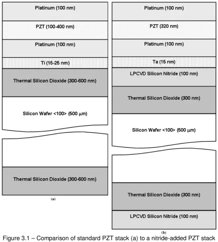
thicknesses can completely compensate for these stresses [42]. Fig. 3.1 shows
the differences between a standard PZT stack process and nitride-added
(a)
(b)
While other researchers have studied issues related to adhesion and quality
of PZT films when nitride is integrated into the process [43-45], this research
investigates a variety of adhesion layers, Zr, ZrO2, Ti, and Ta, and compares
results for each. These adhesion layers were chosen for the following reasons:
(1) Ti is one of the most widely used adhesion layer, (2) Ta has been previously
integrated into silicon nitride applications, and (3) Zr/ZrO2 are similar in chemical
makeup to Ti/TiO2, as they are both considered group IV elements on the
periodic table and are both hard refractory metals.
3.2.
Adhesion Layer Study
Because the applications of this research require extended KOH etch
processes, and because thermal SiO2 films are not effective masks for this
etching process, all test wafers incorporated an LPCVD silicon nitride (Si3N4)
layer as shown in Fig. 3.1b. The bare silicon wafer is initially cleaned using
BakerClean® JTB-111 to ensure that the surface is clear of organic and
particulate contaminants before the subsequent layers are grown or deposited.
The wafer is then placed into an oxidation furnace and thermally oxidized to
create the SiO2 layer. This process exposes the silicon wafer to an oxidizing
environment of O2 or H2O at elevated temperatures (700°C–1300°C), producing
oxide films with thicknesses up to 1.0 µm. This oxidation process is
the presence of oxidizing sources [10], even at low temperatures. The elevated
temperatures used in thermal oxidation serve to accelerate the process. The wet
(H2O as agent) oxidation process was done at 1000°C for 45 min, resulting in 0.3
µm of SiO2. The oxidation reaction is shown below [26]:
+ 2 → 2 + 2
( ) 2 ( ) ( ) 2 ( )
Si solid H O vapor SiO solid H vapor
After oxidation, the wafers were placed into a CVD chamber and LPCVD
nitride was deposited. Various adhesion layers (Zr, Ta, ZrO2, and Ti) were
sputtered onto the silicon nitride. Adhesion layer thicknesses of 15 and 25 nm
were tested to expose any inter-layer diffusion issues. Zr and Ta layers were
deposited using a custom direct current (DC) sputtering system fabricated at the
North Carolina State University Institute for Electroceramic Thin Films. ZrO2 and
Ti were deposited using a customized Advanced Energy RF Sputtering System.
ZrO2 adhesion layers were also achieved via DC sputtering of Zr followed by
oxidation in an open air tube furnace at 600°C for 1 h [43].
After depositing the various adhesion layers, a 100 nm layer of Pt was
deposited via DC sputtering. Next the PZT layers were spin coated at 3000 rpm
for 30 s, and subsequently annealed at 250°C for 5 min. The composition of the
PZT used for this experiment was chosen to be near the morphotropic phase
(x=0.52) and contained excess Pb in order to account for losses during high
process was repeated four times to get the desired thickness of 0.32 µm. After
PZT deposition, the films were annealed for 30 min in a tube furnace at 600 or
650°C by direct insertion to achieve pyrolysis. Finally, the top electrode was
sputtered onto the PZT and capacitors were patterned using a shadow mask.
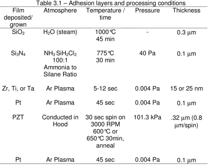
Table 3.1 shows the complete processing conditions for each layer. The
resulting surface quality of each sample was assessed using digital photography
and scanning electron microscopy (SEM), while the ferroelectric characteristics
of the PZT films were assessed using permittivity measurements and polarization
– voltage (P–V) hysteresis loop measurements. The SEM data was acquired
using a JEOL JSM 6400F scanning microscope. The electrical measurements
were taken with an HP4194A impedance analyzer and a RT 6000S ferroelectric
Table 3.1 – Adhesion layers and processing conditions Film
deposited/ grown
Atmosphere Temperature /
time Pressure Thickness
SiO2 H2O (steam) 1000°C
45 min - 0.3 µm
Si3N4 NH3 SiH2Cl2
100:1 Ammonia to Silane Ratio
775°C
30 min 40 Pa 0.1 µm
Zr, Ti, or Ta Ar Plasma 5-12 sec 0.004 Pa 15 or 25 nm
Pt Ar Plasma 45 sec 0.004 Pa 0.1 µm
PZT Conducted in
Hood 30 sec spin on 3000 RPM 600°C or 650°C 30min,
anneal
101.3 kPa .32 µm (0.8 µm/spin)
3.2.1. Zr Adhesion Layer
For the non-oxidized Zr adhesion layer, both the 15 nm and 25 nm layers
failed to withstand the PZT pyrolysis process. Fig. 3.2 shows typical adhesion
layer delamination after pyrolysis. Similar results (not reported here) were
observed for adhesion layer thicknesses of 10–30 nm with PZT pyrolysis
temperatures of 575–700°C.
Figure 3.2 – Delamination in 15 nm Zr adhesion layer with pyrolysis at 600°C
3.2.2. ZrO2 Adhesion Layer
As with the Zr case, the stack structure with a ZrO2 adhesion layer began to
delaminate during pyrolysis. Although this surface delamination would prohibit
integration into a functional MEMS device, it was not as severe as with
3.2.3. Ti Adhesion Layer
Titanium, the most widely used adhesion layer for underlying SiO2 layers, was
deposited via RF sputtering without any high temperature oxidation prior to
depositing the platinum. Although the degree of delamination was less severe
than the Zr samples, it was still severe enough to prevent this adhesion layer
from being integrated into a functional MEMS device.
3.2.4. Ta Adhesion Layer
Tantalum, deposited via DC sputtering with no high temperature oxidation,
was tested next. Fig. 3.3 shows the post pyrolysis surface characteristics of
samples with Ta adhesion layers. These samples exhibited no delamination, and,
with the exception of the non-uniformities associated with spin-on processes,
Figure 3.3 – Surface characteristics of sample made with 15 nm Ta adhesion layer after PZT pyrolysis at 600°C.
Based on this study of various adhesion layers available when incorporating
LPCVD deposited silicon nitride into standard PZT stacks, Ta was the obvious
choice based on its resistance to delamination. While many of the adhesion
layers exhibited adequate polarization and relative dielectric constants (as
discussed in Chapter 4), only samples using tantalum (Ta) adhesion layers
resisted structural delamination. Thus, the Ta adhesion layer samples displayed
defect-free uniform structures.
3.3.
Device Fabrication and Process Flow
Based on the results of the adhesion layer study, a MEMS process was
layer processes of Section 3.2 were the etching and photolithography steps
required to create the membranes.
After oxidation, the wafer was placed into a CVD chamber and LPCVD nitride
was deposited. Square membrane structures, with side lengths of 1.0-4.0 cm,
were patterned onto the back side of the wafer and RIE was used to remove the
silicon nitride and silicon dioxide films and expose the silicon substrate. RIE was
performed using a Semigroup 1000TP Parallel Plate Reactive Ion Etcher and
plasma consisting of Ar/CHF3/O2/SF6 gases. The wafer was then placed into a
heated (80˚C) Potassium Hydroxide (KOH) solution to etch the silicon and create
the desired membrane structure. The thickness of the membrane was monitored
using profilometry until the desired thickness, 10-200 µm, was achieved. This
process is summarized schematically in Figure 3.4 (steps a)-g)) for pure
membrane structures. Similar processes were employed for proof mass
enhanced membranes, as illustrated in Figure 3.5. Not shown in Figures 3.4 and
(a) Bare silicon wafer
(b) Thermal oxidation (3000 Å of SiO2)
(c) LPCVD (1000 Å of Si3N4)
(d) Spin-on, patterning, and exposure of photoresist
(e) RIE to expose silicon and photoresist removal (f) KOH wet etch to create membrane
(g) Deposition of Ta/Pt/PZT/Pt stack on front side
Figure 3.4 – Process description for fabricating silicon membranes in a PZT stack Membrane
Membrane
(a) Bare silicon wafer
(b) Thermal oxidation (3000 Å of SiO2)
(c) LPCVD (1000 Å of Si3N4)
(d) Spin-on, patterning, and exposure of photoresist
(e) RIE to expose silicon and photoresist removal (f) KOH wet etch to create membrane
(g) Deposition of Ta/Pt/PZT/Pt stack on front side
Figure 3.5 – Process description for fabricating proof mass enhanced silicon membranes in a PZT stack
Following etching of the membrane, a 15 nm Ta film was sputtered onto the
front side silicon nitride as described in Section 3.2.4. Sputtering was conducted
using a custom direct current (DC) sputtering system. Then the bottom electrode
Membrane ProofMass
Membrane Proof Mass
(a 100 nm layer of Pt) was deposited onto the Ta film using DC sputtering. Next,
the PZT layers were spin coated using the process described in section 3.2. To
achieve contact with the bottom electrode the outer corners of the membrane
structure were taped off to prevent PZT from being deposited. After PZT
deposition, the films were annealed for 30 minutes in a tube furnace at 650˚C by
direct insertion to achieve pyrolysis. Finally, the top Pt electrode was sputtered
onto the PZT and patterned using a shadow mask creating capacitors over the
membrane. The shadow mask along with the taping off during PZT deposition
allowed access to both the top and bottom electrodes for mechanical and
electrical testing. The process conditions for the device structure were identical
to those summarized in Table 3.1 using a 15 nm Ta adhesion layer.
The above described process was utilized to create the desired membrane
and proof mass enhanced membrane structures. An alternative DRIE process