Available online:
https://edupediapublications.org/journals/index.php/IJR/
P a g e | 20141M.Tech student, Dept. of ECE, Sphoorthy Engineering College,Hyderabad,Telangana, India
2Assistant professor Dept. of ECE, Sphoorthy Engineering College,Hyderabad,Telangana, India
ABST RACT : As technology improves, the power
dissipated by the links of a network-on-chip (NoC) starts to compete with the power dissipated by the other elements of the communicate ion subsystem, namely, the routers and the network interfaces (NIs). Here, we contemporary a set of data encoding schemes to reduce the power dissipated by the links of a NoC. The proposed schemes are designed by Encoder and Decoder block of the system. Then it will be reducing the area of the Encoder and Decoder blocks in NoC.
KEYWORDS- Data encoding, Interconnection on
chip, Network-on-chip (NoC), Modelsim, Verilog.
I. INTRODUCTION
Network on Chip are emerging for the developing the exceptionally dependable for correspondence framework stage. NoC enhances the adaptability of SoCs and the low force of complex SoCs contrasted with different plans. The wires in the connections of the NoC are imparted by numerous signs. As the quality of coordinated frameworks continue growing, a NoC gives enhanced upgraded execution (such as throughput) and adaptability in correlation with past correspondence architectures (e.g., allocated point-to-point signal wires, shared buses or segmented buses with bridges).In existing strategy traditional switch is intended to its related systems through ports. Nowadays, the on-chip communication issues are as relevant as, and in some cases more relevant than, the computation related issues [2]. In fact, the communication subsystem increasingly impacts the traditional design objectives, including cost (i.e., silicon area), performance, power dissipation, energy consumption, reliability, etc. As technology shrinks,
an ever more significant fraction of the total power budget of a complex many-core system-on-chip (SoC) is due to the communication subsystem.
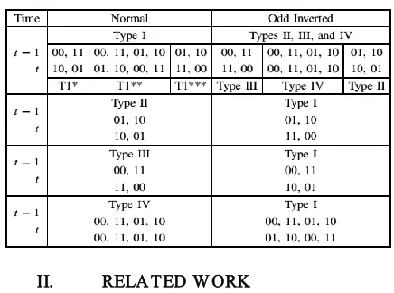
The data encoding techniques are developed to reduce the power consumption caused by the transitions in the interconnect on the chip. The data encoding techniques are based on reducing the number of transitions by considering the types of transitions in the interconnects and by considering them as discussed in the table below and also consider the transitions as different types of inversions available for us. The different types of inversions available for us are odd inversion, full inversion and even inversions. By reducing these inversions we can control the number of transitions in the interconnects which reduces the power consumption caused by these transitions in the links.
Table I: Effect of odd inversion on change of transition types.
II. RELA TED W ORK
Agarwal et al [1] in the upcoming years, the availability of chips with 1000 cores might be seen.
Implementation of Data Encoding Schemes for reducing Power
Available online:
https://edupediapublications.org/journals/index.php/IJR/
P a g e | 2015In these chips, the total system power budget has a
ignificant fraction of dissipation only by interconnection networks. Hence, the design of power-efficient interconnection networks has been the focus of many works in the literature dealing with NoC architectures. The focus of this paper is on reducing the power dissipated by the links, some works in reducing the power is surveyed below. These include the techniques that make use ofnpassive shielding which is used to reduce the capacitive coupling effects of adjacent bus lines by inserting passive ground or power lines between them.
Stan et al. [2] presented Bus-Invert method ofcoding which helps in lowering the I/O bus activity and thus decreases the I/O peak power dissipation by 50% and the I/O average power dissipation is up to 25% [2]. This decreases the performance when tradeoff is made between performance and power dissipation. The number of transitions from 0 to 1 for two consecutive flits (the flit that just traversed and the one which is about to traverse the link) is counted. If the number is larger than half of the link width, the inversion will be performed to reduce the number of 0 to 1 transitions when the flit is transferred via the link. This technique is only concerned about the self-switching without worrying the coupling self-switching.
Ramprasad et al. [3] a source coding framework is presented which describes encoding schemes to reduce transition activity. t is based on obtaining a prediction function and a prediction error. This prediction error is XORed with the previous value sent to the bus so that the number of transitions is reduced.
Musoll et al. [4] Working zone encoding (WZE) presents a method for encoding an external address bus. Without instruction and data caches, this scheme is beneficial for data address and shared buses, cases which that have the largest number of bus transitions and for which other coding are less effective. The major drawback of the WZE is its larger encoder and decoder logic overhead, which limits the benefits of the I/O activity reduction.
Jantsch et al. [5] analyzed the use of partial bus invert coding as link level low power encoding technique with the conclusion that it spends several times more power than no encoding at all, if normalized for the same performance, which is done by adjusting supply voltage and frequency.
A coding technique that reduces the coupling switching activity by taking the advantage of end to-end encoding for wormhole switching has been presented in [6]. It is based on lowering the coupling switching activity by eliminating only Type II transitions.
Kwang et al [7] Coupling effects between on-chip interconnects must be addressed in ultra-deep submicron VLSI and system-on-a-chip (SoC) designs. A new low-power bus encoding scheme is proposed to minimize coupled switching which dominate the on-chip bus power consumption. The coupling-driven bus inverts method use slim encoder and decoder architecture to minimize the hardware overhead.
Pande et al. [8] proposed the use of cross talk avoidance codes (CAC) to improve the signal integrity by reducing the effective coupling capacitance and lowering the energy dissipation of wire segments [8]. By incorporating CAC in NoC data streams the effective coupling capacitance of the inter-switch wire segments and hence the communication energy is reduced without incurring the non-optimal wire area overhead of shielding/spacing. However, its application requires redundant wires and the encoding/decoding process is performed hop by hop for the header flit In another coding technique presented in [8], bunches of four bits are encoded with five bits. The encoded bits were isolated using shielding wires such that the occurrence of the patterns “101” and “010” were prevented.
III. THE PROPOSED A PPROA CHES
Available online:
https://edupediapublications.org/journals/index.php/IJR/
P a g e | 2016activities and interconnection network. The dynamic
power dissipated by the interconnects band drivers is
P=[T0→1(CS+Cl)+TCCC]V2 Fck………)
where T 0→1 is the number of 0 transitions in the bus in two consecutive transmissions, Tc is the number of correlated switching between physically adjacent lines, Cs is the line to substrate capacitance, Cl is the load capacitance, C is the coupling capacitance, Vdd is the supply voltage, and Fck is the clock frequency. A Type I transition occurs when one of the lines switches when the other remains unchanged.
In a Type II transition, one line switches from low to high while the other makes transition from high to low. A Type III transition corresponds to the case where both lines switch simultaneously. Finally, in a Type IV transition both lines does not change. The coupling transition activity, Tc, is a weighted sum of different types of coupling transition contributions. Therefore we can write it as:
TC =K1T1+K2T2+K3T3+K4T4 ………. (2)
Using (2), one may express (1) as
P = [T0→1(Cs+Cl) +(T1+2T2)Cc]v2Fck……. (3)
PαT0→1Cs+(T1+2T2)Cc……… (4)
We calculate the occurrence probability for different types of transitions. Consider that flit (t −1) and flit (t) refer to the previous flit which was transferred the link in the flit respectively. We consider only two adjacent bits of the physical channel. Sixteen different combinations of these four bits could occur (Table I). The first bit is the value of the generic ith line of the link, whereas the second bit represents the value of its (i +1)th line. The number of transitions for Types I, II, III, and IV are 8, 2, 2, and 4, respectively. For a random set of data, each of these sixteen transitions has the same probability.
Therefore, the occurrence probability in Types I, II, III, and IV are 1/2, 1/8, 1/8, and 1/4, respectively.
A . Sch eme I: In scheme I, we focus on reducing the numbers of Type I transitions and Type II by converting in to type1. The scheme compares the current data with the previous one to decide whether odd inversion or no inversion of the current data can lead to the link power reduction.
P’αT0→1+ (K1T1’+K2T2’+K3T3’+K4T4’) CC……… (5)
1) Po wer M o d el: If the flit is odd inverted dynamic power on the link in the self-transition activity, and the coupling transition before being transmitted, the activity of Types I, II, III, and IV, respectively. Table I reports. The first bit is the value of the generic ith line of the link, whereas the second bit represents the value of it’s (i+1)th line.
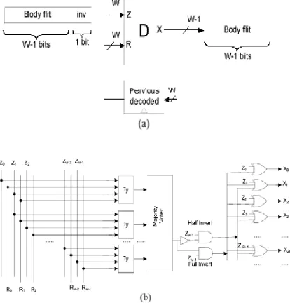
Fig.1(a) Encoder architecture scheme1 circuit diagrams
Available online:
https://edupediapublications.org/journals/index.php/IJR/
P a g e | 2017Fig.2 Encoder architecture Scheme II
Full and odd inversion based this advanced encoding architecture consist of w-1 link width and one bit for inversion bit which indicate if the bit travel through the link is inverted or not. W bits link width is considered when there is no encoding is applied for the input bits. Here the TY block from scheme 1 is added in scheme 2. This takes two adjacent bits from the given inputs. From these two input bits the TY block checks what type of transitions occurs.
T2 > T4** ………. (7)
We have T2 and T4** blocks which determines if any of the transition types T2 and T4**occur based on the link power reduction. The number of ones blocks in the next stage. The output of the TY, T2 and T4** send through the number of one‘s blocks. The output of the ones block is log 2 w. The first ones block is used to determine the number of transitions based on odd inversion. The second ones block determines the number of transitions based on the full inversion and the then another one ones block is used to determine the number of transitions based on the full inversion. These inversions are performed based on the link power reduction. Based on these ones block the Module A takes the decision of which inversion should be performed for the link power reduction. For this
module is satisfied means the output is set to ‘1‘. None of the output is set to ‘1‘ if there is no inversion is takes place. The module A is implemented using full adder and comparator circuit.
The block diagram of the decoder is shown in Fig.3. The w-1 bits input is applied in the decoder circuit and another input of the decoder is previous decoded output. The decoder block compares the two input data‘s and inversion operation is performed and w-1 bits output is produced. The remaining one bit is used to indicate the inversion is performed or not. Then the decoder output is given to the gray to binary block. This block converts the gray code into original binary input.
In decoder circuit diagram (Fig.4.) consist of TY block and Majority vector and XOR circuits. Based on the encoder action the TY block is determined the transitions. Based on the transitions types the majority blocks checks the validity of the inequality given by (2).
Available online:
https://edupediapublications.org/journals/index.php/IJR/
P a g e | 2018The output of the majority voter is given to the
XOR circuit. Half inversion, full inversion and no inversion is performed based on the logic gates.
Sch eme III: In scheme III, we are adding the even inversion into scheme II. Because the odd inversion converts Type I transitions into Type II transitions. From table II, T1**/T1*** are converted into Type IV/Type III transitions by the flits is even inverted. The link power reduction in even inversion is larger than the Odd inversion.
Fig.4. Encoder architecture for scheme III
The encoding architecture (Fig.4) in scheme III is same of encoder architecture in scheme I and II. Here we are adding the Te block to the scheme II. This is based on even invert condition, Full invert condition and Odd invert condition. It consists of w-1 link width input and the w bit is used for the inversion bit. The full, half and even Inversion is performed means the inversion bit is set ‘1‘, otherwise it set as ‘0‘.The TY, Te and T4** block determines the transition types T2, Te and T4**. The transition types are sending to the number of ones block. The Te block is determined if any of the detected transition of types T2, T1** and T1**. The ones block determines the number of ones in the corresponding transmissions of TY, T2, Te and T4**. These numbers of ones is given to the Module C block. This block check if odd, even, full or no invert action corresponding to the outputs ‘10‘, ‘01‘, ‘11‘ or ‘00‘ respectively, should be
performed. The decoder architecture of scheme II and scheme III are same.
IV RESULT A ND DISCUSSION
Fig.5, 6 and 7 shows the simulation result of scheme I,II III (Type I (T1***) using encoding techniques. In scheme II the number of type II transition is converted into Type IV transitions by using the odd and full inversion condition.Fig.8.9 and 10 shows the synthesis results of Scheme I,II and III (Type I(T1*** ) Decoder block output.
Fig.5 Scheme I
Available online:
https://edupediapublications.org/journals/index.php/IJR/
P a g e | 2019Fig.7 Scheme III
Fig. 8 Scheme I Synthesis
Fig. 9 Scheme II Synthesis
Fig. 10 Scheme III Synthesis
IV. CONCLUSION
Available online:
https://edupediapublications.org/journals/index.php/IJR/
P a g e | 2020REFERENCES
[1] D. Yeh, L. S. Peh, S. Borkar, J. Darringer, A. Agarwal, and W. M. Hwu, “Thousand core chips roundtable,” IEEE Design Test Comput., vol. 25,no. 3, pp. 272–278, May– Jun. 2008.
[2] M. R. Stan and W. P. Burleson, “Bus-invert coding for low-power I/O,” IEEE Transaction Very Large Scale Int (VLSI) Sys vol. 3, no. 1,pp. 49–58, Mar. 1995.
[3] S. Ramprasad, N. R. Shanbhag, and I. N. Hajj, “A coding framework for low-power address and data busses,” IEEE Trans. Very Large Scale Integr. (VLSI) Syst., vol. 7, no. 2, pp. 212–221, Jun. 1999.
[4] M. Palesi, G. Ascia, F. Fazzino, and V. Catania, “Data encoding schemes in networks on chip,” IEEE Transac. Computer-Aided Design Int.Circuits Sys, vol. 30, no. 5, pp. 774–786, May 2011.
[5] S. Youngsoo, C. Soo-Ik, and C. Kiyoung, “Partial bus-invert coding for power optimization of application-specific systems,” IEEE Trans. Very Large Scale Integr. (VLSI) Syst., vol. 9, no. 2, pp.377–383, Apr. 2001.
[6] R. Ayoub and A. Orailoglu, “A unified transformational approach for reductions in fault vulnerability, power, and crosstalk noise and delay on processor buses,” in Proc. Design Autom. Conf. Asia South Pacific, vol.2. Jan. 2005, pp. 729–734.
[7] Z. Yan, J. Lach, K. Skadron, and M. R. Stan, “Odd/even bus invert with two-phase transfer for buses with coupling,” in Proc Int. Symp. LPower Electron. Design, 2002, pp. 80–83.
[8] C. P Fan and C. H. Fang, “Efficient RC low power bus encoding methods for crosstalk reduction,” Integrated VLSI vol. 44, no. 1,pp. 75– 86, Jan. 2011. [9] L.Macchiarulo, E. Macii, and M. Poncino, “Wire placement for crosstalk energy minimization in address buses,” in Proc. Design Autom. Test Eur. Conf. Exhibit., Mar. 2002, pp. 158–162.
Bio Data
A u th o r
N.Karu n akar currently pursuing M.Tech in Electronics and Communication Engineering in Dept. of ECE, Sphoorthy Engineering College, Hyderabad, Telangana, India.
Co -A u th o r