Design of Dual Redundancy Can-Bus
Controller with Very Efficient Memory
Controller
Neelam.Sravani & S.A.Vara Prasad
M.tech(VLSI),Depatment of ECE,BVC College of Engineering,Rajamahendravaram,A.P,India
[email protected]
Assistant.professor, Depatment of ECE,BVC College of Engineering,Rajamahendravaram,A.P,India
[email protected]
Abstract—At present, the strategy of double excess CAN-bus is fundamentally executed by programming, with the goal that it has the impediments of low quality and terrible continuous execution. Based on the error taking care of control in CAN particular adaptation 2.0, an equipment excess administration unit is inventively advanced in this paper. In view of FPGA, a sort of redid Dual Redundancy CAN-bus Controller (DRCC) is planned. By downloading the IP Core into a XILINX's SPARTAN-3 chip to test, it has been confirmed that the plan could totally meet the prerequisite for high continuous execution and unwavering quality, with a brilliant prospect for what's to come
Keywords—Dual Redundancy CAN-bus; Verilog; FPGA; IP Core
I. INTRODUCTION
With the improvement of EDA (Electronic Design Automation), advanced framework outlined by FPGA is broadly utilized as a part of a wide range of fields [1], for example, correspondence, aviation, therapeutic medications and mechanical control framework [7]. CAN (Controller Area network) has turned out to be a standout amongst the most well-known information transport [2] with attributes, for example, hostile to impedance capacity, much lower cost and simple upkeep. There are an incredible number of CAN chips in market for instance
PHILIPS' SJA1000 [3]. Regardless of how flawless the single-channel CAN bus system is, while something happens to the single-channel bus system, for example, short out or open circuit, the entire system won't work. To take care of this issue, a few ideas of repetition were advanced before. To aggregate up, there are three sorts of methods for excess information transport [4, 6, 8, 9, 10]. The first is excess of transport driver, which utilizes one CPU, one CAN controller and two transport drivers. The second is repetition of transport controller, which utilizes one CPU, two CAN controllers and two
transport drivers. The latter is excess of
II. DUAL REDUNDANCY CAN-BUS (DRC) NETWORK ARCHITECTURE
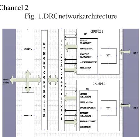
The DRC Arrange design is appeared in Fig.1. Contrasted and physical layer of a solitary transport CAN Network, physical layer of the DRC System is included an extra channel. In single-bus CAN arrange, if its exclusive channel is seriously meddled or open, the System will be ruined. In any case, the DRC System's physical layer has two totally autonomous channels, which are Channel 1 and Channel 2 separately. In the event that the excess administration neglects to transmit message from one channel, it will transmit the message naturally from the other channel.
III. DUAL REDUNDANCY CAN-BUS
CONTROLLER DESIGN
A. DRCC Structure The piece graph of DRCC is appeared in Fig.2. DRCC is made out of good for nothing Stream Processor Squares (BSPB), one Repetition Administration Piece (RMB) and two Smash Pieces. The BSPB incorporates one state-machine and one Piece Timing Rationale Square (BTLB). The capacity of a few squares RI DRCC can be portrayed as takes after: BTLB [12] screens the serial CAN-transport line, deals with the transport line-related piece timing, does hard synchronization and resynchronization, makes up for the proliferation defer times and controls the specimen point and the quantity of tests to be taken inside a bit time. BSPB assumes responsibility of Date Connection Layer convention and oversees CAN Message, for example, perceiving and dealing
with standard edge and augmented casing,
overseeing FIFO and separating Message and etc.
Channel 1
Channel 2
Fig. 1.DRCnetworkarchitecture
Fig. 2. Dual Redundancy CAN-bus Controller Block Diagram
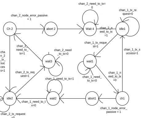
Ch 2 ch1 abort1 wait2 idle2 wait1 wait3 idle1 Wait 4 abort 2 chan_1_need_to_t x=0 chan_1_node_error_ passive = 1 chan_2_tx_request =0 cha n_2 _tx_ suc ces s=1 chan_2_node_error_passive = 1 chan_2_need_to_tx= 0 chan_2_n eed_to_tx =1 chan_1_tx_re quest=0 chan_1_tx_s uccess=1 chan_1_tx_reque st=1 chan_2_need _to_tx=0 chan_1_need_ to_tx=0 chan_1_n eed_to_tx =0 chan_2_ need_to_ tx=1 chan_2_tx_req uest=1 chan_1_need_to_tx=1
Fig. 3. State transition diagram
Two RAMs are used to buffer messages waiting for being communicated, to buffer received messages and to register all kinds of states which DRCC runs.
B. Excess administration state-machine The RMB incorporates three state-machines, a principle state machine and two assistant state-machines. The state move chart of primary state-machine is appeared in Fig.3 and its each state is portrayed in Table 1.The two RAMs are utilized to cushion messages sitting tight to be imparted, to cradle got messages and to enroll a wide range of states which DRCC runs.
TABLE I. STATE DESCRIPTION STATE FUNCTION DESCRIPTION
idle1 reset state idle1 state
If system has some messages to send, first write the messages to buffer, and then set the
chan_1_tx_request. When the main state-machine monitors this change, starts transmitting process and changes to wait1 state.
wait1 wait1 state If Channel1 isn’t ready for transmitting message, the state-machine will still wait. Otherwise, change to ch1 state.
ch1 channel 1 send state
If Channel 1 transmits a message successfully, the state-machine returns to idle1 state and will be ready for transmitting next message from the Channel1. Otherwise, the state-machine changes to abort1 state in order to abort the message which wasn’t transmitted successfully from Channel 1.
abort1 channel 1 abort state
The state-machine sets chan_1_abort_send signal of Channel 1, and then changes to wait2 state
Wait 2
Wait 2 State
If abort the corrupted message from Channel 1 successfully, the state-machine changes to idle2 state in order to transmit the same message from Channel 2. Otherwise, will still wait.
idle2 idle2 state
If The past state is wait2 state, the state-machine is directly into wait3 state. Or else, the state-machine needs to wait for chan_2_tx_request signal which is the request signal of Channel 2.
Wait 3 Wait 3 State If Channel 2 isn’t ready for sending message, the state-machine will still wait. Otherwise, changes to ch2 state.
ch2 channel 2 send state
If Channel 2 transmits successfully, the state-machine returns to idle2 state and will be ready for next message from the Channel2. Otherwise, the state-machine changes to abort2 state in order to abort the corrupted message from Channel 2.
abort2 abort state The state-machine sets chan_2_abort_send signal of Channel 2, and then changes to wait4 state.
IV. DRCC SIMULATION TEST
Among these tests, the DRCC IP core [13] is used as a component as if it was a chip in a Printed Circuit Board (PCB). Block diagram of
the test system is shown in Fig.4. Task of the test program includes computing the expected
timing of DRCC interface, writing read/write function and writing test bench [15, 16].
Fig. 4. Test system block diagram
A. Transmission error count and transmission
prepare Reproduction consequences of the
connection between transmission error check and transmission process are appeared in Fig.5. As appeared in Fig.5, while transmitting sign is HIGH, a message is currently transmission. The flag transport of tx_err_cnt[7:0] is a pointer of transmission mistake counter, which will increment by 8 for every transmission disappointment. While transmission mistake counter is more than 80Hex, the transmitting message of Channel1 is prematurely ended.
B. Transmission error number and mistake
uninvolved enactment The consequences of
recreation of a connection between transmission mistake check and blunder detached initiation is appeared in Fig.6. While transmission blunder
counter (chan_a_bsp_tx_err_cnt[8:0]) is more
noteworthy than 80Hex, the flag of Mistake
Detached (chan_a_bsp_node_error_passive) is
initiated. In repetition mode, the state-machine will begin the way toward exchanging channel.
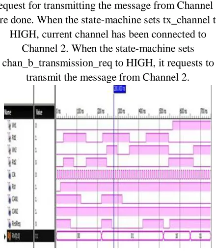
C. Switching channels the results of simulation of switching channels are shown in Fig.7.
1) Step 1: At the point when
chan_a_transmission_req is inspected HIGH amid a clock cycle, the state-machine begins transmission of a message from Channel 1. Because of affirmation mistake, the message neglects to be transmitted from Channel 1 and this prompts to expand transmission
blunder counter (chan_a_bsp_tx_err_cnt). As
indicated by the lead in CAN particular form 2.0, the tainted message is naturally retransmitting when the transport is sit out of gear again [5]. This implies the debased message is more than once transmitted until achievement or Blunder Uninvolved actuation. As a result, transmission blunder counter keeps on expanding. 2) Stage 2: When transmission blunder counter is more noteworthy than 80Hex, the flag of Mistake Detached (chan_a_bsp_node_error_passive) is enacted. This demonstrates Channel 1 is severely corrupted.
3) Step 3: In this phase, switching channel and request for transmitting the message from Channel 2 are done. When the state-machine sets tx_channel to
HIGH, current channel has been connected to Channel 2. When the state-machine sets chan_b_transmission_req to HIGH, it requests to
transmit the message from Channel 2.
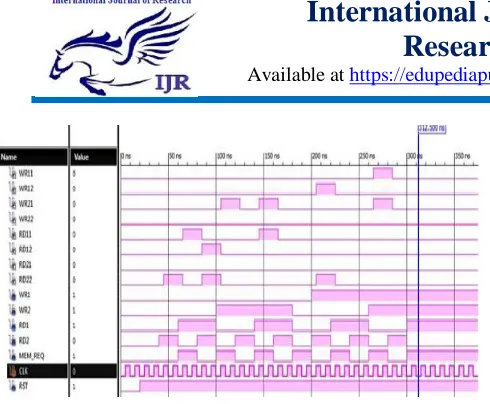
Fig 6 simulation result for memory controller with CAN bus controller
4) Stage 3: In this stage, exchanging channel and demand for transmitting the message from Channel 2 are finished. At the point when the state-machine sets tx channel to HIGH, current channel has been associated with Channel 2. At the point when the state-machine sets chan_b_transmission_req to HIGH, it solicitations to transmit the message from Channel 2.
5) Stage 4: flag of transmission_ack. At the point when the message is effectively transmitted, the state-machine sets the flag to a clock period.
6) Stage 5: flag of tx_sucess. At the point when the message is effectively transmitted, the state-machine sets the flag to a clock period.
D. Channel trading time As showed up in Fig.8, in the midst of 25ms or close, Channel 1 (node1_tx1_i) transmitted on and on a message however did not accomplishment. This leaded to mistake Idle incitation and subsequently a comparative message is changed to Channel 2 to transmit. Channel 2 (node1_tx2_i) completes viably transmission just once. Thusly, Channel trading time needs 25ms or so under the perceive botch condition.
V. CONCLUSIONS
The Dual Redundancy CAN Controller core,
which is simulated and synthesizable, can be
used as a component in a project and it must
have had a bright prospect for the future. The
memory controller is added to CAN bus for
efficient controlling. By downloading the IP
Core into a XILINX’s VERTEX - 6 chip to test,
the design of Dual Redundancy CAN-bus
Controller Based on memory controller is
successful. It guarantees reliability and real-time
performance
and
compensates
for
the
disadvantage of software redundancy.
Design summary report for memory controller
CAN bus controller
REFERENCES
[1] Ma Xiaojun, Tong Jiarong, “Design and
Implementation of A New FPGA Architecture,” ASIC, 2003. Proceedings.5th International Conference, Vol.2, pp.816-819, October 2003.
[2] Yu Zhu, Can and FPGA Communication Engineering: Implementation of a Can Bus Based Measurement System on an Fpga Development Kit, DiplomicaVerlag, 2010. [3] Philips Semiconductors. SJA1000 Standalone CAN controller. January 2000.
[4] Qing Jia, DeviceNet media redundancy㧘iCC 2005.
[5] Robert Bosch GmbH, CAN Specification Version 2.0, September 1991.
[6] Jos´eRufino, Dual-Media Redundancy Mechanisms for CAN, Technical Report, January 1997.
[7] CiA - CAN in Automation. CAN Physical Layer for Industrial Applications - CiA/DS102-1, April 1994. [8] C. Mateus, Design and implementation of a non-stop Ethernet with a redundant media interface. Graduation Project Final Report, Instituto Superior T´ecnico, Lisboa, Portugal, September 1993. (inportuguese).
[9] Han Ju, Ke Jing, Jin Jiang, A kind of CAN bus
redundancy method, Electronics Process
Technology(China), Vol.19, No.4, 1999.
[10] Yu ChunLai, XuHuaLong, Liu GengWang, HouXiaoLing, Research of the Redundant Methods of CAN, Measurement & Control Technology(China), Vol.22, No.10, 2003.
[11] Xilinx Inc, Spartan-3 FPGA Family: Complete Data Sheet, May 2007.
[12] I. Mohor, CAN Core, Complete Data Sheet, May 2007.
[13] Jane Smith, Verilog Coding Guidelines, Cisco Systems, Inc.
[14] M.A. Livani, J. Kaiser, and W.J. Jia, Scheduling hard and soft real-time communication in CAN, In Proc. of the 23rd.Workshop on Real-Time Programming, Shantou, China, June 1998.IFAC/IFIP.
[15] Lattice Semiconductor Corporation, A Verilog HDL Test Bench Primer: Application Note.
[16] AbhishekShetty, Hamid Mahmoodi, System Verilog Testbench Tutorial, Nano-Electronics & Computing Research Center School of Engineering San Francisco State University San Francisco, C'A Fall 2011.
[17] S. Punnekkat, H. Hansson, and C. Norstrom, “Response time analysis under errors for CAN”, Proceedings of the IEEE Real-Time Technology and Applications Symposium, pp. 258-265, Washington, USA, May 2000.
[18] Robert I. Davis, Alan Burns, Controller Area