International Journal of Research (IJR)
e-ISSN: 2348-6848, p- ISSN: 2348-795X Volume 2, Issue 07, July 2015Available at http://internationaljournalofresearch.org
Performance Analysis of Five Port Router Network for VLSI
based Network on Chip
1
chalavadi Raghavendrarao,
PG Student, Sri Krishnadevaraya Engg College,NH-44,GOOTY,ANANTAPURAM (DIST), ANDHRA PRADESH,,PIN-515401
2
S.T.Mrudula
M.tech., Sri Krishnadevaraya Engg College, NH-44,GOOTY,ANANTAPURAM (DIST),
ANDHRA PRADESH,,PIN-515401
Abstract
In his paper we attempt to give a networking solution by applying VLSI architecture techniques to router design for networking systems to provide intelligent control over the network. Networking routers today have limited input/output configurations, which we attempt to overcome by adopting bridging loops to reduce the latency and security concerns. Other techniques we explore include the use of multiple protocols. We attempt to overcome the security and latency issues with protocol switching technique embedded in the router engine itself. The approach is based on hardware coding to reduce the impact of latency issues as the hardware itself is designed according to the need. We attempt to provide a multipurpose networking router by means of Verilog code, thus we can maintain the same switching speed with more security as we embed the packet storage buffer on chip and generate the code as a self-independent VLSI Based router. Our main focus is the implementation of hardware IP router. The approach enables the router to process multiple incoming IP packets with different versions of protocols simultaneously, e.g. for IPv4 and IPv6. The approach will results in increased switching speed of routing per packet for both current trend protocols, which we believe would result in considerable enhancement in networking systems.
LANGUAGE USED: VERILOG HDL
Keywords--Network-on-Chip ;Simulation Router; FIFO; FSM; Register blocks
1.
INTRODUCTION
Shifting from a silicon technology node to the next one results in faster and more power efficient gates but slower and more power hungry wires. In fact, more than 50% of the total dynamic power is dissipated in interconnects in current processors, and this is
expected to rise to 65%–80% over the next several
International Journal of Research (IJR)
e-ISSN: 2348-6848, p- ISSN: 2348-795X Volume 2, Issue 07, July 2015Available at http://internationaljournalofresearch.org
the intrinsic delay of a two-input NAND fanout of 5.
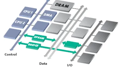
If the raw computation horsepower seems to be unlimited, thanks to the ability of instancing more and more cores in a single silicon die, scalability issues, due to the need of making efficient and reliable communication between the increasing number of cores, become the real problem. The networkon- chip (NoC) design paradigm is recognized as the most viable way to tackle with scalability and variability issues that characterize the ultradeep submicronmeter era.
Nowadays, the on-chip communication issues are as relevant as, and in some cases more relevant than, the computationrelated issues. In fact, the communication subsystem increasingly impacts the traditional design objectives, including cost (i.e., silicon area), performance, power dissipation, energy consumption, reliability, etc. As technology shrinks,
an ever more significant fraction of the total power budget of a complex many-core system-on-chip (SoC) is due to the communication subsystem.
A number of research studies have demonstrated the feasibility and advantages of Network-on-Chip (NoC) over traditional bus-based architectures. This whitepaper summarizes the limitations of traditional bus-based approaches, introduces the advantages of the generic concept of NoC, and provides specific data about Arteris‟ NoC, the first commercial implementation of such architectures. Using a generic design example we provide detailed comparisons of scalability, performance and area of traditional busses or crossbars vs. Arteris‟ NoC.
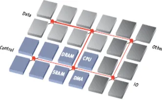
1.1 NOC ARCHITECTURE:
The advanced Network-on-Chip developed by Arteris employs system-level network
techniques to solve onchip traffic transport and management challenges. As discussed in the previous section and shown in Figure a, synchronous bus limitations lead to system segmentation and tiered or layered bus architectures.
Figure a: Traditional synchronous bus
Contrast this with the Arteris approach illustrated in Figure 2. The NoC is a homogeneous, scalable switch fabric network,This switch fabric forms the core of the NoC technology and transports multi-purpose data packets within complex, IP-laden SoCs. Key characteristics of this architecture are:
Layered and scalable architecture
Flexible and user-defined network topology.
International Journal of Research (IJR)
e-ISSN: 2348-6848, p- ISSN: 2348-795X Volume 2, Issue 07, July 2015Available at http://internationaljournalofresearch.org
Figure b: Arteris switch fabric network
1.2 NOC LAYERS
IP blocks communicate over the NoC using a three layered communication scheme (Figure 3), referred to as the Transaction, Transport, and Physical layers
Figure c : Arteris NoC layers
The Transaction layer defines the communication primitives available to interconnected IP blocks. Special NoC Interface Units (NIUs), located at the NoC periphery, provide transaction-layer services to IP blocks with which they are paired. This is analogous, in data communications networks, to Network Interface Cards that source/sink information to the LAN/WAN media. The transaction layer defines how information is exchanged between NIUs to implement a particular transaction. For example, a NoC
transaction is typically made of a request from a master NIU to a slave NIU, and a response from the slave to the master. However, the transaction layer leaves the implementation details of the exchange to the transport and physical layer. NIUs that bridge the NoC to an external protocol (such as AHB) translate transactions between the two protocols, tracking transaction state on both sides. For compatibility with existing bus protocols, Arteris NoC implements traditional address-based Load/ Store transactions, with their usual variants including incrementing, streaming, wrapping bursts, and so forth. It also implements special transactions that allow sideband communication between IP Blocks.
The Transport layer defines rules that apply as packets are routed through the switch fabric. Very little of the information contained within the packet (typically, within the first cell of the packet, a.k.a header cell) is needed to actually transport the packet. The packet format is very flexible and easily accommodates changes at transaction level without impacting transport level. For example, packets can include byte enables, parity information, or user information depending on the actual application requirements, without altering packet transport, nor physical transport.
1.3NOC LAYERED APPROACH
BENEFITS
A summary of the benefits of this layered approach are:
International Journal of Research (IJR)
e-ISSN: 2348-6848, p- ISSN: 2348-795X Volume 2, Issue 07, July 2015Available at http://internationaljournalofresearch.org
application requirements, while the physical layer is mostly influenced by Silicon process characteristics. Thus the layered architecture enables independent optimization on both sides. A typical physical optimization used within NoC is the transport of various types of cells (header and data) over shared wires, thereby minimizing the number of wires and gates.
Scalability. Since the switch fabric deals only with packet transport, it can handle an unlimited number of simultaneous outstanding transactions (e.g., requests awaiting responses). Conversely, NIUs deal with transactions, their outstanding transaction capacity must fit the performance requirements of the IP Block or subsystems that they service. However, this is a local performance adjustment in each NIU that has no influence on the setup and performance of the switch fabric.
Aggregate throughput. Throughput can be increased on a particular path by choosing the appropriate physical transport, up to even allocating several physical links for a logical path. Because the switch fabric does not store transaction state, aggregate throughput simply scales with the
operating frequency, number and width of switches and links between them, or more generally with the switch fabric topology.
Quality Of Service. Transport rules allow traffic with specific real-time requirements to be isolated from best-effort traffic. It also allows large data packets to be interrupted by higher priority packets transparently to the transaction layer.
1.4 ROUTER:
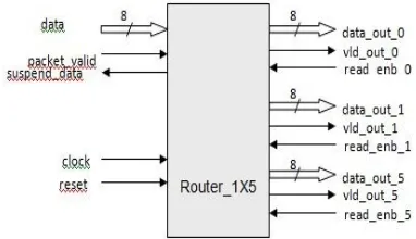
Router is a packet based protocol. Router drives the incoming packet which comes from the input port to output ports based on the address contained in the packet. The router has a one input port from which the packet enters. It has three output ports where the packet is driven out. The router has an active low synchronous input reset which resets the router.
Fig d. Block Diagram of Router_1X5
1.4.1 Router_1X5Architecture:
This design consists of 6 main blocks. Which are fsm_router, router_reg, ff_sync, and 3 fifo. The fsm_router block
International Journal of Research (IJR)
e-ISSN: 2348-6848, p- ISSN: 2348-795X Volume 2, Issue 07, July 2015Available at http://internationaljournalofresearch.org
the control signals provided by the fsm_router. There are 3 fifo for each output port, which stores the data coming from input port based on the control signals provided by fsm_router module. The ff_sync module provides synchronization between fsm_router module and 3 fifo s , So that single input port can faithfully communicate with 3 output ports.
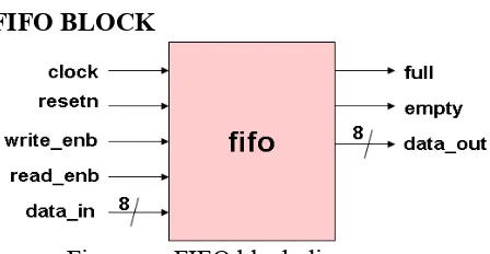
FIFO BLOCK
Figure e : FIFO block diagram
There are 3 fifos used in the router design. Each fifo is of 8 bit width and 16 bit depth. The fifo works on system clock. It has synchronous input signal reset. If resetn
is low then full =0, empty = 1 and data_out = 0
Write operation:
The data from input data_in is sampled at rising edge of the clock when input write_enb is high and fifo is not full.
Read Operation:
The data is read from output
data_out at rising edge of the clock, when
read_enb is high and fifo is not empty. Read and Write operation can be done simultaneously.
Full – it indicates that all the locations inside fifo has been written.
Empty – it indicates that all the locations of fifo are empty.
This module provides synchronization between fsm and fifo modules. It provides faithful communication between single input port and three output ports. It will detect the address of channel and will latch it till packet_valid is asserted, address and write_enb_sel will be used for latching the incoming data into the fifo of that particular channel. A fifo_full output signal is generated, when the present fifo is full, and fifo_empty output signal is generated by the present fifo when it is empty.
If data = 00 then fifo_empty =
empty_0 and fifo_full = full_0
If data = 01 then fifo_empty =
empty_1 and fifo_full = full_1
If data = 10 then fifo_empty =
empty_2 and fifo_full = full_2
Else fifo_empty = 0 and fifo_full = 1.
The output vld_out signal is generated when empty of present fifo goes low, that means present fifo is ready to read.
vld_out_0 = ~empty_0
vld_out_1 = ~empty_1
International Journal of Research (IJR)
e-ISSN: 2348-6848, p- ISSN: 2348-795X Volume 2, Issue 07, July 2015Available at http://internationaljournalofresearch.org
write_enb signal for the present fifo which is selected by present address..
If resetn is low then output (dout, err, parity_done and low_packet_valid) are low. The output parity_done is high
when the input ld_state is high and (fifo-full and packet_valid) is low
or when the input laf_state and output low_packet_valid both are high and the previous value of parity_done is low. It is reseted to low value by reset_int_reg signal. The output low_packet_valid is high
when the input ld_state is high and packet_valid is low.
It is reseted to low by reset_int_reg signal.
First data byte i.e., header is latched inside the internal register first_byte when
detect_add and packet_valid signals are high, So
that it can be latched to output dout when
lfd_state signal goes high.Then the input data
i.e., payload is latched to output dout if ld_state
signal is high and fifo_full is low. Then the input data i.e., parity is latched to output dout if
lp_state signal is high and fifo_full is low.
The input data is latched to internal register full_state_byte when ld_state and
fifo_full are high; this full_state_byte data is
latched inside the output dout when laf_state
goes high.Internal parity register stores the parity calculated for packet data, when packet is transmitted fully, the internal calculated parity is compared with parity byte of the packet. An
error signal is generated if packet parity is not equal to the calculated parity.
Figure(f): FSM Block
The „fsm_router‟ module is the controller circuit for the router. This module generates all the control signals when new packet is sent to router. These control signals are used by other modules to send data at output, writing data into the fifo.
Functionality:
On reset router fsm(finite state machine) will be in DECODE ADDRESS State.
DECODE ADDRESS State:
In this state if packet_valid = 1,data_in<3,and fifo_empty = 1 then circuit jumps to LOAD_FIRST_DATA.
In DECODE ADDRESS State if packet_valid = 1,data_in<3,and fifo_empty = 0 then circuit goes to WAIT_TILL_EMPTY.
WAIT_TILL_EMPTY State:
In this state if fifo_empty = 0 then circuit remains in the same state i,e WAIT_TILL_EMPTY State.
If fifo_empty = 1 then circuit goes to the LOAD_FIRST_DATA State.
LOAD_FIRST_DATA State:
International Journal of Research (IJR)
e-ISSN: 2348-6848, p- ISSN: 2348-795X Volume 2, Issue 07, July 2015Available at http://internationaljournalofresearch.org
By default the circuit will be in LOAD_ DATA State.
If fifo_full = 0,and packet_valid = 0,then the circuit goes to LOAD_PARITY state.
If fifo_full = 1, then the circuit goes to FIFO_FULL_ STATE.
LOAD_ PARITY State:
If fifo_full = 0 then the circuit goes to CHECK_PARITY_ERROR.
If fifo_full = 1 then the circuit goes to FIFO_FULL_ STATE.
FIFO_FULL_ STATE state:
If fifo_full = 1 then the circuit remains in the same state i,e FIFO_FULL_ STATE.
If fifo_full = 0 then the circuit goes to the state called as i,eLOAD_AFTER_FULL STATE.
CHECK_PARITY_ERROR state:
If the circuit reaches to unconditional criteria then the circuit goes to DECODE ADDRESS State.
LOAD_AFTER_FULL state:
In this state if parity_done = 0,and low_packet_valid = 1 then the circuit goes to a state called as LOAD_PARITY state.
If parity_done = 0,and low_packet_valid = 0 then the circuit goes to a state called LOAD_DATA state.
STATE - DECODE_ADDRESS
This is the default state. It waits for the
packet_valid assertion, After packet_valid signal
goes high, if the address is valid and fifo for that address is empty (fifo_empty signal will be high), data can be loaded, so, it goes to the next
state LOAD_FIRST_DATA. If fifo is not empty it goes to WAIT_TILL_EMPTY so that, new data couldn‟t be accepted till fifo is ready. The output signal detect_add is made high, so that ff_sync module can detect the address of fifo to be used. detect_add signal is also used by router_reg module to latch the first byte in internal register.
STATE - LOAD_FIRST_DATA
In this state lfd_state signal is generated, which indicates to the router_reg module that first data byte can be latched.At the same time
suspend_data signal is made high so that first
data byte can be faithfully latched inside the output data register in router_reg module. In the next clock edge unconditionally this state is changed to LOAD_DATA.
STATE - LOAD_DATA
In this state data is latched inside the data registers of router_reg module, for this ld_state
signal is generated for router_reg module.
suspend_data signal is made low, so that router
can accept the new data from input simultaneously, latched data is sent to the fifo
and write_enb_reg is generated for writing into
present fifo. If fifo_full input goes high then no more data can be accepted by router so it goes to FIFO_FULL_STATE. Data is latched till the packet_valid signal is asserted, when it is de-asserted in LOAD_DATA state, it goes to LOAD_PARITY state, where last parity byte is latched..
STATE – FIFO_FULL_STATE
International Journal of Research (IJR)
e-ISSN: 2348-6848, p- ISSN: 2348-795X Volume 2, Issue 07, July 2015Available at http://internationaljournalofresearch.org
low. Signal full_state is generated for router_reg module. This state changes to LOAD_AFTER_FULL state when fifo_full becomes low..
STATE – WAIT_TILL_EMPTY
In this state neither new data is accepted nor data is latched by router_reg module, So
suspend_data signal is made high and
write_enb_reg signal is made low. It waits for
the fifo_empty signal, when it goes high, it goes
to the LOAD_FIRST_DATA state.
STATE – CHECK_PARITY_ERROR
In this state reset_int_reg signal is generated, which resets the status and parity registers inside the router_reg module. Neither any data is latched nor any input data is accepted. Router_reg compares the data parity from packet with calculated parity during this state.This state changes to default state DECODE_ADDRESS with next clock edge.
OPERATION:
The Five Port Router Design is done by using of the three blocks. The blocks are 8-Bit Register, Router Controller and output block. The router controller is design by using FSM design and the output block consists of four FIFO‟s combined together. The FIFO‟s store data packets and when you want to send data that time the data will read from the FIFO‟s. In this router design has four outputs i.e. 8-Bit size and one 8-bit data port. It is used to drive the data into router. we are using the global clock, reset signals, error signal and suspended data signals are the output‟s of the router. The FSM controller gives the error and SUSPENDED_DATA_IN signals.
These functions are discussed clearly in below FSM description. The ROUTER can operate with a single master device and with one or more slave devices. If a single slave device is used, the RE (read enable) pin may be fixed to logic low if the slave permits it. Some slaves require \the falling edge (HIGH→LOW transition) of the slave select to initiate an action such as the mobile operators, which starts conversion on said transition. With multiple slave devices, an independent RE signal is required from the master for each slave device.
Figure (g): Internal Structure of Protocol
2. SIMULATION RESULTS:
2.1 RTL SCHEMATIC FOR FIVE PORT ROUTER:
International Journal of Research (IJR)
e-ISSN: 2348-6848, p- ISSN: 2348-795X Volume 2, Issue 07, July 2015Available at http://internationaljournalofresearch.org
2.3 TECHNOLOGY SCHEMATIC FOR FIVE PORT ROUTER:
2.4 SIMULATION RESULTS:
2.5 Device Utilization Summary
3. CONCLUSION & FUTURE
SCOPE
In this paper, we have presented a set of new data encoding schemes aimed at reducing the power dissipated by the links of an NoC. In fact, links are responsible for a significant fraction of the overall power dissipated by the communication system. In addition, their contribution is expected to increase in future technology nodes. As compared to the previous encoding schemes proposed in the literature, the rationale behind the proposed schemes is to minimize not only the switching activity, but also (and in particular) the coupling switching activity which is mainly responsible for link power dissipation in the deep submicron meter technology regime. The proposed encoding schemes are agnostic with respect to the underlying NoC architecture in the sense that their application does not require any modification neither in the routers nor in the links. An extensive evaluation has been
carried out to assess the impact of the encoder and decoder logic in the NI. The encoders implementing the proposed schemes have been assessed in terms of power dissipation and silicon area. The impacts on the performance, power, and energy metrics have been studied using a cycle- and bitaccurate NoC simulator under both synthetic and real traffic scenarios. Overall, the application of the proposed encoding schemes allows savings up to 51% of power dissipation and 14% of energy consumption without any significant performance degradation and with less than 15% area overhead in the NI.we analyze the efficacy of the proposed data encoding schemes on two complex heterogeneous systems.
International Journal of Research (IJR)
e-ISSN: 2348-6848, p- ISSN: 2348-795X Volume 2, Issue 07, July 2015Available at http://internationaljournalofresearch.org
In future there is a chance to estimate the power consumption also. The first one, which is mapped to an 8 × 8 mesh, consisted of a triple video object plane decoder which has 38 cores (D 38 tvopd) and multimedia and wireless communication which has 26 cores (D 26 media). We assumed a minimum of two-flit and maximum eight-flit packets, deterministic XY routing, and input FIFO buffers of four flits. The time distribution of the traffic followed Poisson‟s distribution while random data sets were used as workloads.
4. REFERENCES
[1] International Technology Roadmap for Semiconductors. (2011) [Online]. Available:
http://www.itrs.net
[2] M. S. Rahaman and M. H. Chowdhury, “Crosstalk avoidance and errorcorrection coding for coupled RLC interconnects,” in Proc. IEEE Int. Symp. Circuits Syst., May 2009, pp. 141–144.
[3] W. Wolf, A. A. Jerraya, and G. Martin, “Multiprocessor system-on-chip MPSoC technology,” IEEE Trans. Comput.-Aided Design Integr. CircuitsSyst., vol. 27, no. 10, pp. 1701–1713, Oct. 2008.
[4] L. Benini and G. De Micheli, “Networks on chips: A new SoC paradigm,” Computer, vol. 35, no. 1, pp. 70–78, Jan. 2002.
[5] S. E. Lee and N. Bagherzadeh, “A variable frequency link for a poweraware network-on-chip (NoC),” Integr. VLSI J., vol. 42, no. 4, pp. 479–485, Sep. 2009.
[6] D. Yeh, L. S. Peh, S. Borkar, J. Darringer, A. Agarwal, andW. M. Hwu, “Thousand-core chips roundtable,” IEEE Design Test Comput., vol. 25, no. 3, pp. 272–278, May–Jun. 2008.
[7] A. Vittal and M. Marek-Sadowska, “Crosstalk reduction for VLSI,” IEEE Trans. Comput.-Aided Design Integr. Circuits Syst., vol. 16, no. 3, pp. 290– 298, Mar. 1997.
[8] M. Ghoneima, Y. I. Ismail, M. M. Khellah, J. W. Tschanz, and V. De,
“Formal derivation of optimal active shielding for low-power on-chip buses,” IEEE Trans. Comput.-Aided Design Integr. Circuits Syst., vol. 25, no. 5, pp. 821–836, May 2006.
[9] L. Macchiarulo, E. Macii, and M. Poncino, “Wire placement for crosstalk energy minimization in address buses,” in Proc. Design Autom. Test Eur. Conf. Exhibit., Mar. 2002, pp. 158–162.
[10] R. Ayoub and A. Orailoglu, “A unified transformational approach for reductions in fault vulnerability, power, and crosstalk noise and delay on processor buses,” in Proc. Design Autom. Conf. Asia South Pacific, vol. 2. Jan. 2005, pp. 729–734.
[11] K. Banerjee and A. Mehrotra, “A power-optimal repeater insertion methodology for global interconnects in nanometer designs,” IEEE Trans. Electron Devices, vol. 49, no. 11, pp. 2001–2007, Nov. 2002.
[12] M. R. Stan and W. P. Burleson, “Bus-invert coding for low-power I/O,” IEEE Trans. Very Large Scale Integr. (VLSI) Syst., vol. 3, no. 1, pp. 49–58, Mar. 1995.
[13] S. Ramprasad, N. R. Shanbhag, and I. N. Hajj, “A coding framework for low-power address and data busses,” IEEE Trans. Very Large Scale Integr. (VLSI) Syst., vol. 7, no. 2, pp. 212–221, Jun. 1999.
International Journal of Research (IJR)
e-ISSN: 2348-6848, p- ISSN: 2348-795X Volume 2, Issue 07, July 2015Available at http://internationaljournalofresearch.org
[15] L. Benini, G. De Micheli, E. Macii, D. Sciuto, and C. Silvano, “Asymptotic zero-transition activity encoding for address busses in low-power microprocessor-based systems,” in Proc. 7th Great Lakes Symp. VLSI, Mar. 1997, pp. 77–82.
[16] E. Musoll, T. Lang, and J. Cortadella, “Working-zone encoding for reducing the energy in microprocessor address buses,” IEEE Trans. Very Large Scale Integr. (VLSI) Syst., vol. 6, no. 4, pp. 568–572, Dec. 1998.
[17] W. Fornaciari, M. Polentarutti, D. Sciuto, and C. Silvano, “Power optimization of system-level address buses based on software profiling,” in Proc. 8th Int. Workshop Hardw. Softw. Codesign, May 2000, pp. 29–33.
[18] L. Benini, G. De Micheli, E. Macii, M. Poncino, and S. Quer, “Power optimization of core-based systems by address bus encoding,” IEEETrans. Very Large Scale Integr. (VLSI) Syst., vol. 6, no. 4, pp. 554–562, Dec. 1998.
[19] L. Benini, A. Macii, M. Poncino, and R. Scarsi, “Architectures and synthesis algorithms for power-efficient bus interfaces,” IEEE Trans.Comput.-Aided Design Integr. Circuits Syst., vol. 19, no. 9, pp. 969– 980, Sep. 2000.
[20] G. Ascia, V. Catania, M. Palesi, and A. Parlato, “Switching activity reduction in embedded systems: A genetic bus encoding approach,” IEE Proc. Comput. Digit. Tech., vol. 152, no. 6, pp. 756–764, Nov. 2005.
[21] R. Siegmund, C. Kretzschmar, and D. Muller, “Adaptive Partial Businvert encoding for power efficient data transfer over wide system buses,” in