ISSN (Print) : 2320 – 3765 ISSN (Online): 2278 – 8875
I
nternational
J
ournal of
A
dvanced
R
esearch in
E
lectrical,
E
lectronics and
I
nstrumentation
E
ngineering
(An UGC Approved Journal)
Website: www.ijareeie.com
Vol. 6, Issue 8, August 2017
A High Step-Up DC-DC Converter Using
Photovoltaic System Based On Integrating
Coupled Inductor and Switched Capacitor
Techniques
Keerti, Dr. Sangamesh Sakri
M. Tech Student, Department of Power Electronics, Poojya Doddappa Appa College of Engineering, Gulbarga, India
Department of Power Electronics, Poojya Doddappa Appa College of Engineering, Gulbarga, India
ABSTRACT: In this paper a high voltage gain Dc to Dc converter is proposed using a switched capacitor and coupled inductor for renewable energy applications. It consists of switched capacitor, coupled inductor, voltage multiplier cell. Switched capacitor gets charged in off period by utilizing the energy accumulated in the coupled inductor which increases the voltage transfer gain. In the proposed topology the voltage stress on the main power switch is also minimized. Therefore, the conduction losses is reduced by using low resistance RDS(ON) with main power switch. The
simulation model of “A High Step-Up Dc-Dc Converter Using Photovoltaic System Based On Integrating Coupled Inductor and Switched Capacitor Techniques” is developed using MATLAB software for the input 40v from the PV panel, output voltage across the load 530v and power 354W. Finally, to check its performance the prototype circuit with a 12v input voltage and 180V output voltage is conducted.
KEYWORDS: High voltage gain, DC-DC converter, Switched capacitor technique, coupled inductor, Renewable energy.
I. INTRODUCTION
Due to diminishing availability of fossil fuel, an increase in energy demand, the future is looking towards optional power sources all of which will need to be regulated in one Form or another. To make this possible, a highly efficient low cost product will have to be designed. Among all the different varieties of converter designs high power with high efficiency can be achieved only by few converters. The basic switched –mode dc to dc converters along with buck-boost, buck, buck-boost, cuk, zeta and sepic have been utilized in different electronic applications because of their many advantages such as high efficiency, simple structure, good performance, simple control unit and simple design. The boost converters are used to get high voltage from low voltage. The high voltage converters are popularly used in various industry applications, such as photovoltaic systems, electric vehicles, high intensity discharge lamps and fuel cell system.
ISSN (Print) : 2320 – 3765 ISSN (Online): 2278 – 8875
I
nternational
J
ournal of
A
dvanced
R
esearch in
E
lectrical,
E
lectronics and
I
nstrumentation
E
ngineering
(An UGC Approved Journal)
Website: www.ijareeie.com
Vol. 6, Issue 8, August 2017
based converter. However the energy accumulated in the leakage inductor leads to a voltage spike on the main switch and worsens the conversion efficiency. To overcome this issue active clamping circuits with coupled inductor based converters are presented. High step up converter with two switch and single switch are explained. As number of switches increases losses will be increased. However the conversion ratio is not large enough. Thus to overcome these disadvantages a new concept “A High Step-Up Dc-Dc Converter Using Photovoltaic System Based on Integrating Coupled Inductor and Switched Capacitor Techniques” is proposed.
In this work a high step up Dc to Dc converter using photovoltaic system based on integrating coupled inductor and capacitor techniques. The structure comprises of a two voltage multiplier cells and coupled inductor in order to produce high step up voltage gain. In addition a capacitor gets charged during the switch-off time by utilizing the energy accumulated in the coupled inductor which raises the voltage transfer gain. By the help of a passive clamp circuit the energy stored in the leakage inductance is recycled and voltage stress on the main power switch is also minimized in the proposed topology. Therefore, to reduce the conduction losses a main power switch with low resistance RDS (ON) is
utilized.
II. LITERATURE SURVEY
Some transformer-based converter like forward, push-pull or fly back converter can achieve high step-up voltage gain by adjusting the turn ratio of the transformer. However, the leakage inductor of the transformer will cause serious problem such as voltage spick on the main switch and high power dissipation. In Order to improve these drawbacks non dissipative snubbed circuits and an active clamp circuits are used. However, the cost will be increased due to the extra power switch and high side driver.
Switched capacitor and voltage lift techniques have been widely used to achieve high step-up voltage gain. However, in these structures, high charging current will flow through the main switch and increase the conduction losses.
Coupled-inductor based converter can also achieve high step-up voltage gain by adjusting the turn ratios. However, the energy stored in the leakage inductor causes a voltage spike on the main switch and deteriorates the conversion efficiency.
In order to find a better solution to the above problem, a high step-up dc-dc converter for renewable energy application is proposed.
III. METHODOLOGY
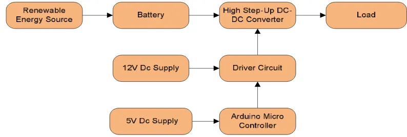
In the Fig.1 the input is taken as Dc voltage from the renewable energy source. The different renewable energy sources are wind, fuel cells, hydropower, geothermal, biomass etc.
ISSN (Print) : 2320 – 3765 ISSN (Online): 2278 – 8875
I
nternational
J
ournal of
A
dvanced
R
esearch in
E
lectrical,
E
lectronics and
I
nstrumentation
E
ngineering
(An UGC Approved Journal)
Website: www.ijareeie.com
Vol. 6, Issue 8, August 2017
For this work photovoltaic system is chosen as source. Power which is generated by the solar is extracted and it is conserved in the battery. The charged battery will give the constant output of voltage and current. The output of the battery is not suitable for the high voltage application. So, battery is allied to the high step up dc-dc converter. The turning ON switch and OFF the switch which is in dc-dc converter is controlled through arduino microcontroller. Microcontroller is utilized as a control unit to produce pulses to the power switches of the converter. For the conversion of low voltage to high voltage a high step up DC to DC converter is utilized. The output of the DC to Dc converter is allied to the resistive load.
3.1. Proposed High Step-Up Converter
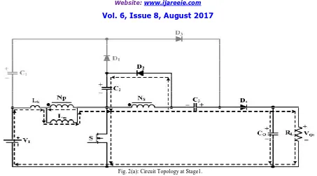
The circuit diagram of the proposed and developed converter circuit is shown in Fig.2. The proposed converter consists of a coupled inductor, Dc input voltage (VI), active power switch(S), four capacitors and four diodes. Clamp
circuit is designed by using and diode .In a voltage multiplier cell is act as a extended capacitor. The voltage multiplier consists of capacitor C2 and diode D2 circuit elements and voltage multiplier enhance the voltage of clamping
capacitor. The coupled inductor is designed as an ideal transformer including leakage inductor Lk, magnetizing
inductor Lm turns ratio N (NP/NS).Some assumptions are considered to simplify the circuit design analysis, as follow:
1. VC1, VC2, VC3 and V0 are constant during the switching period due to the large size of the capacitors.
2. The leakage inductance of the coupled inductor is accepted even when all the components are ideal.
By considering the above mentioned assumptions, the Continuous Conduction Mode (CCM) operation of the proposed converter is presented below.
Fig.2: High Step-Up DC-DC Converter Circuit Diagram.
It consists of one switching period with five stages of conduction. Operating elements can be accomplished by five stages, that five stages are shown in the below explanation.
Stage 1[t0<t<t1]: In the first stage, switch S is made active. Also, diodes D 2 and D4 are made active by making diodes
D1, D3
inactive. DC source (VI) magnetizes L m through S. By the use of diode , the capacitor is connected parallel with
the secondary side of the coupled inductor.
The secondary side current of the coupled inductor (iS) gets decreases linearly when leakage inductor current
gets enhances linearly. The output capacitor supplies the required energy of load ( ). When secondary –side of the coupled inductor current reaches zero at t= this interval gets completed. At stage1 the circuit topology is shown in Fig.2 (a).
ISSN (Print) : 2320 – 3765 ISSN (Online): 2278 – 8875
I
nternational
J
ournal of
A
dvanced
R
esearch in
E
lectrical,
E
lectronics and
I
nstrumentation
E
ngineering
(An UGC Approved Journal)
Website: www.ijareeie.com
Vol. 6, Issue 8, August 2017
Fig. 2(a): Circuit Topology at Stage1.
Stage 2 [t2<t<t3]: In the second stage, switch S is made active and also diode D3 are made active by making diodes D1,
D 2 and D4 inactive. The DC source VI magnetizes Lm through switch S. So, the magnetizing inductor with leakage
inductor gets enhanced linearly. The dc source
V I, clamp capacitor and the secondary-side of the coupled
Inductors are used to charge the capacitor .The demanded energy of the load is supplied by output capacitor . This interval completes when switch(S) is turned inactive at t=t2. At stage2 the circuit topology is shown in Fig.2 (b).
Fig. 2(b): Circuit Topology at Stage2.
Stage 3 [t2<t<t3]: In the third stage, switch S is made inactive. Diodes D1 and D3 are turned active by making diodes D2
and D4 are inactive. The stored energy in capacitor , magnetizing inductor Lm, and the energies of leakage inductor
Lk are utilized to charge clamp capacitor
.The currents of the secondary-side of the coupled inductor (iS) and the leakage inductor are enhanced and reduced
ISSN (Print) : 2320 – 3765 ISSN (Online): 2278 – 8875
I
nternational
J
ournal of
A
dvanced
R
esearch in
E
lectrical,
E
lectronics and
I
nstrumentation
E
ngineering
(An UGC Approved Journal)
Website: www.ijareeie.com
Vol. 6, Issue 8, August 2017
This interval completes when leakage inductor current and Magnetizing inductor current both are equal( iLk is equal to
iLm) at t=t3.
At stage 3 the circuit topology is shown in Fig.2(c).
Fig.2(c): Circuit Topology at Stage3.
Stage 4 [t3<t<t4]: In the fourth stage, switch S is turned inactive. Diodes D1 and D4 are turned active by making diodes
D2 and D3 are turned inactive. The capacitor , magnetizing inductor Lm, and the energies of leakage inductor Lk is
utilized to charge clamp capacitor . The leakage inductor current and Magnetizing inductor current both are reduce linearly. Also, the secondary side of the coupled inductor stores a part of the energy stored in Lm.. The output capacitor
is charged by dc source VI, capacitor C3 and both sides of the coupled inductor and produces energy to the load RL.
This interval completes when diode D1 is turned inactive, at t=t4. At stage 4 the circuit topology is shown in Fig.2 (d).
Fig.2 (d): Circuit Topology at Stage4.
Stage 5 [t4<t<t5]: In the fifth stage, switch S is turned inactive. Diodes D2 and D4 are turned active by making diodes D1
and D3 are turned inactive. The leakage inductor (Lk) current and Magnetizing inductor (Lm) current both are reduce
ISSN (Print) : 2320 – 3765 ISSN (Online): 2278 – 8875
I
nternational
J
ournal of
A
dvanced
R
esearch in
E
lectrical,
E
lectronics and
I
nstrumentation
E
ngineering
(An UGC Approved Journal)
Website: www.ijareeie.com
Vol. 6, Issue 8, August 2017
this is done through D2 diode. The output capacitor is charged by DC input voltage VI and stored energy in the
capacitor C3 and inductances of both sides of the coupled inductor and produces the demand energy of the load RL.
This interval completes when switch S is turned active at t=t5. At stage 5 the circuit topology is shown in Fig.2 (e).
Fig.2 (e): Circuit Topology at Stage 5.
The timing diagram and key waveforms are shown in Fig 3.
ISSN (Print) : 2320 – 3765 ISSN (Online): 2278 – 8875
I
nternational
J
ournal of
A
dvanced
R
esearch in
E
lectrical,
E
lectronics and
I
nstrumentation
E
ngineering
(An UGC Approved Journal)
Website: www.ijareeie.com
Vol. 6, Issue 8, August 2017
IV. SIMULATION OUTPUT
4.1 Simulation Model
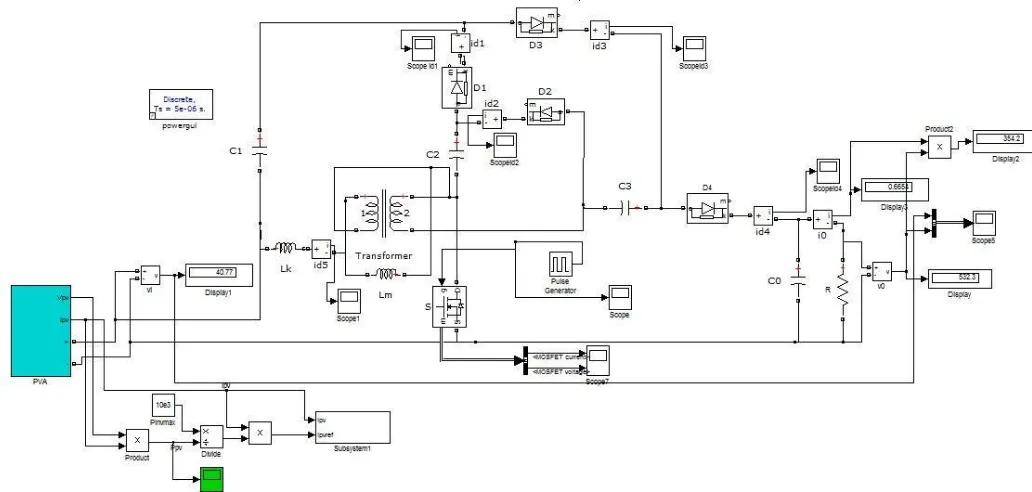
The simulated proposed system using MATLAB Simulink tool is shown in the following Fig.4.Table.1 shows the simulation outputs for various input voltages. From Fig.5 to 9 shows the voltage and current waveforms of the switches.
Fig.4: Simulation Model of Proposed Converter
Table 1: Input and Output Voltage Table
Sl. No Input Voltage(V) Output Voltage(V)
1 12 157
2 15 197
3 20 264
4 25 331
5 30 398
6 35 465
ISSN (Print) : 2320 – 3765 ISSN (Online): 2278 – 8875
I
nternational
J
ournal of
A
dvanced
R
esearch in
E
lectrical,
E
lectronics and
I
nstrumentation
E
ngineering
(An UGC Approved Journal)
Website: www.ijareeie.com
Vol. 6, Issue 8, August 2017
Fig..5: Output Voltage at an Input of 12V
Fig..6: Output Voltage at an Input of 15V
ISSN (Print) : 2320 – 3765 ISSN (Online): 2278 – 8875
I
nternational
J
ournal of
A
dvanced
R
esearch in
E
lectrical,
E
lectronics and
I
nstrumentation
E
ngineering
(An UGC Approved Journal)
Website: www.ijareeie.com
Vol. 6, Issue 8, August 2017
Fig.8: pulse of the power switch
Fig.9 output waveform for the switch S1
4.2 Experimental Setup
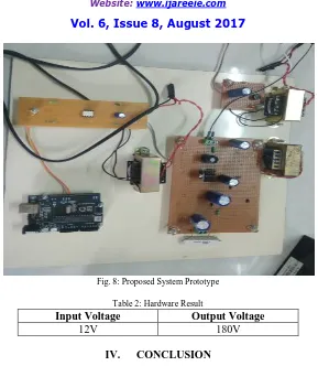
The feasibility of the proposed converter is confirmed by building experimental prototype. The developed converter hardware has been made and verified in power electronics laboratory.
ISSN (Print) : 2320 – 3765 ISSN (Online): 2278 – 8875
I
nternational
J
ournal of
A
dvanced
R
esearch in
E
lectrical,
E
lectronics and
I
nstrumentation
E
ngineering
(An UGC Approved Journal)
Website: www.ijareeie.com
Vol. 6, Issue 8, August 2017
Fig. 8: Proposed System Prototype
Table 2: Hardware Result
Input Voltage Output Voltage
12V 180V
IV. CONCLUSION
A high step-up dc/dc converter using Photovoltaic System based on integrating coupled inductor and switched capacitor techniques. By utilizing switched capacitor, the energy accumulated in the leakage inductance of the coupled inductor is recycled. The voltage stress across the main switch is decreased. Here the gate signals are produced using PWM control schemes. Finally, a hardware prototype is implemented which converts the 12V input voltage into 180V output voltage. By considering the low input current ripple and low conduction losses this converter is characterized, Voltage stress on the main power switch is decreased. This converter is very useful inPhotovoltaic systems, Fuel cell system, Electric vehicles, and High intensity discharge lamps applications. The results prove the feasibility of the presented converter.
REFERENCES
[1] Yi-ping Hsieh, and Jainn-Fuh Chen, “Novel High Step-Up DC-DC Converter with Coupled-Inductor and Switched –Capacitor Techniques for a Sustainable Energy System”, IEEE, Vol. 26, No. 12, 2011.
[2] Ian-Hsieng Lee and Tsorng-Juu Liang, “Isolated Coupled-Inductor-Integrated DC-DC Converter with Non dissipative Snubber for Solar Energy Applications”, IEEE, Vol. 61, 2014.
[3] Yi ZhaoandYunjie Gu, “Single-Phase High Step-up Converter With Improved Multiplier Cell Suitable for Half- Bridge-Based PV Inverter System”, IEEE, Vol. 29, 2014.
[4] Tsorng - Juu Liang, “Novel Isolated High-Step-Up DC–DC Converter with Voltage Lift”, IEEE, Vol. 60, 2013.
[5] Peyman Saadat and Karim Abbaszadeh, “A Single Switch High step up DC-DC Converter Based on Quadratic Boost”, IEEE, 2016. [6] Kuo-Ching Tseng, Chi-Chih Huang, and Wei-Yuan Shih, “A High Step-Up Converter with a Voltage Multiplier Module for a Photovoltaic