dangling bond states at ultrathin Si–SiO
2interfaces
A. P. Younga)
Department of Electrical Engineering, The Ohio State University, Columbus, Ohio 43210-1272
J. Scha¨fer
Center for Materials Research, The Ohio State University, Columbus, Ohio 43210-1272
G. H. Jessen
Department of Electrical Engineering, The Ohio State University, Columbus, Ohio 43210-1272
R. Bandhu
Department of Physics, The Ohio State University, Columbus, Ohio 43210-1272
L. J. Brillson
Department of Electrical Engineering, Center for Materials Research, and Department of Physics, The Ohio State University, Columbus, Ohio 43210-1272
G. Lucovsky and H. Niimi
Department of Material Science and Engineering, North Carolina State University, Raleigh, North Carolina 27695-8202
~Received 21 January 1998; accepted 28 May 1998!
We have directly observed cathodoluminescence ~CL!in ultrahigh vacuum over a broad spectral range ~0.7–4.0 eV! from ultrathin 5 nm layers of remote plasma enhanced chemical vapor deposition grown a-SiO2:H deposited on silicon substrates. In the infrared regime, luminescence is observed at 0.8 eV, consistent with the presence in the as-deposited film of Si dangling bond localized states, as well as at 1.1 eV due to band edge emission. In the optical regime, three peaks ~1.9, 2.7, and 3.4 eV! are observed showing evidence for band tail state emission from an amorphous silicon–oxygen bonded suboxide region in the film, with smaller contributions from either substrate related c-Si or defect containing, stoichiometric SiO2. CL spectra with a range of beam voltages indicate that the stoichiometric SiO2 is very close to the free surface of the film, possibly due to oxidation of the air-exposed wafer or due to a nonuniformity in the film. When the films are annealed in situ in stages up to 500 °C, we observe no change in the shape of the a-SiOx:H peak at 1.9 eV, showing the stability of this suboxide to such temperatures. These observations are consistent with CL measurements of thicker films of a-SiO2:H and a-SiOx, and demonstrate the utility of CL spectroscopy for the study of ultrathin dielectric studies. © 1998 American Vacuum
Society.@S0734-211X~98!11904-2#
I. INTRODUCTION
Si–SiO2 interfaces are a subject of both fundamental in-terest as well as being extremely important to the perfor-mance of electronic devices, notably, metal–oxide– semiconductor ~MOS! type structures. Recently gate linewidths have shrunk deep into the submicron regime and, if the scaling laws of electronic devices continue to hold, oxide thicknesses must shrink as well. For amorphous SiO2, the current oxide used in MOS structures to remain as a viable insulating material, the thickness of this layer must decrease to 3 nm or less in future generation devices.
At the Si–SiO2interface, it is well known that a silicon-rich suboxide 0.4–0.6 nm thick exists between the stoichio-metric amorphous SiO2 (a-SiO2) and the crystalline Si (c-Si) substrate.1As the thickness required of the oxide shrinks to the point where a significant fraction of the sub-oxide is part of the interface, detailed knowledge correlating
the chemical and electrical properties of the interface be-comes of increasing importance to the performance of the device.
Because the thickness of the transition layer is so thin, it is difficult to easily deconvolute the electronic properties of the suboxide from the rest of the ‘‘bulk’’ stoichiometric ox-ide. Photoinduced luminescence is difficult with conven-tional sources, given the large band gap of SiO2~9.1 eV!and of other dielectrics.2Cathodoluminescence ~CL! and photo-luminescence ~PL! spectroscopies have been used to study the electronic properties of bulk~;1mm!SiO2films,
3,4 thick ~;1 mm! SiOx films,5–7 as well as oxidized porous silicon structures.8 While CL has been extensively used for the study of bulk SiO2, to our knowledge, we know of no posi-tive CL results for extremely thin, homogeneous, silicon di-oxide films. In this work, we present what we believe is the first spectroscopic CL measurements of ultrathin~5 nm!SiO2 films on Si substrates.
II. EXPERIMENT
The SiO2films were initially grown with a;0.5 nm oxide layer prepared by in situ plasma-assisted oxidation onto p-type silicon wafers in a multichamber UHV system for both oxides and dielectrics. On top of this layer, the 5-nm-thick, hydrogenated SiO2 (a-SiO2:H! films were deposited by re-mote plasma enhanced chemical vapor deposition ~RPECVD!. Additional details of the vacuum chamber appa-ratus and the growth process have been described elsewhere.9–11All the films were then transported through air to a separate UHV chamber with a base pressure of ;1 – 2 310210 Torr for CL analysis.
The Si–SiO2 films were measured by CL at room tem-perature and T;90 K. As shown schematically in Fig. 1, an electron gun employing voltages and currents in the range 0.6–4.5 keV and ;1.0–4.0mA, respectively, was used for the generation of the luminescence. The electron beam is incident on the sample at an angle of 45° with a spot diam-eter of;200–500mm. A liquid nitrogen cooled North Coast
p-i-n Ge detector measured the luminescence in the spectral
range 0.7–2.0 eV, while a thermoelectrically cooled S-20 photomultiplier tube ~PMT! was used to measure the lumi-nescence in the range 1.4–4.0 eV.
The Leiss monochromator employed contains a flint glass prism with nominally 50 meV resolution over the measure-ment range from the near infrared through the near ultravio-let ~UV! part of the spectrum. For the in situ annealing ex-periments, the specimens were rapidly brought up to temperature ~;1 min!, held for 5 min at 400 °C or 500 °C, then brought back to room temperature for analysis. During the annealing process, the specimen temperature was mea-sured using an infrared pyrometer. The CL spectra presented here have not been corrected for the spectral responsivity dependence of the detector or the transmission of the optical train.
III. RESULTS
Even though the a-SiO2:H film was only 5 nm thick, the luminescence was strong enough to be faintly visible to the naked eye at room temperature. The light appeared white, with blue and red components mixed in. Besides providing quantitative luminescence spectra for the wide band gap ma-terials, CL has another distinct advantage over optical exci-tation techniques, namely, a large variable exciexci-tation depth controllable via the incident electron beam energy. Figure 2 shows spectra from the as-deposited specimen for various excitation voltages ~0.6–4.5 keV!with discrete peaks appar-ent in the visible and near UV region of the electromagnetic spectrum. There is an obvious change in spectral features as a function of beam energy. The low energy spectra at 0.6 and 1.0 keV show broad luminescence peak features centered at 2.7 and 1.9 eV. When the beam intensity is increased from 1.5 up to 4.5 keV, the features change dramatically, with a much broader band centered at 1.9 eV and a weak peak developing at 3.4 eV, which increases with increasing beam voltages.
The temperature dependence of the luminescence can help to clarify the stoichiometry and bonding arrangements of the various forms of Si and SiOx in the film, since the luminescence from a-Si is known to be strongly quenched, while a-SiOx:H does not show this behavior. As can be seen in Fig. 3, after lowering the temperature of the as-deposited film to 90 K, the overall spectrum shape did not change significantly; there was only a minor intensity increase.
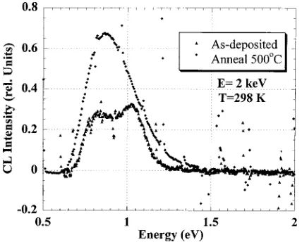
In addition to the spectra in the visible and the UV, the infrared spectrum is shown in Fig. 4 for the as-deposited film at an excitation voltage of E52 keV. Two peaks were clearly resolved at;0.8 and;1.0 eV. The infrared spectrum at 2 keV was typical. For voltages between 0.6 and 3.0 keV, the only significant change observed was an increase in the relative intensity of the 1.0 eV band compared to the 0.8 eV band as the excitation voltage increased. Also shown in Fig.
FIG. 1. Schematic diagram of the experimental apparatus showing the rela-tive orientation of the electron gun, the in situ lens, and the external optical
4 is the CL spectrum after the specimen was annealed in 5 min stages in situ up to 500 °C. In Fig. 4, it is clear that there is dramatically enhanced intensity at 0.8 eV after the anneal-ing compared to the as-deposited case.
Figure 5 shows the corresponding visible/UV spectrum as a function of annealing temperature for the same excitation voltage. In contrast with the strong increase in luminescence in the infrared, there is relatively little change in intensity observed in the visible region of the spectrum. The only significant change that we observed is the slight strengthen-ing of the 3.4 eV band as the annealstrengthen-ing progresses.
We also addressed the possibility of electron-beam dam-age of the film. During our experiments, the incident beam delivers ;milliwatt over ;1023cm2. Given the relatively high thermal conductivity of the p-doped substrate and the minimal thickness of the SiO2 overlayer, this input power
should not produce any significant thermal damage, espe-cially in comparison to bulk SiO2studies. In addition, for a 2 keV beam energy with a current of 1mA, the total exposure is on the order of 1017 electrons/cm2, two orders of magni-tude below the reported damage threshold for a thicker SiO2 film.12For our experiment for possible damage, a typical CL spectrum was measured, then the beam was allowed to re-main on one spot for 2 h, and the spectra was then remea-sured. As can be seen in Fig. 6, there is only a minor change in the intensity of the 1.9 eV peak. These spectral changes are within the limits of reproducibility of our experiment. Typical CL spectra are obtained with over an order of mag-nitude lower exposure ~flux times time!, so that damage should not be a significant problem for this system with these short~;12 min!exposure times and currents.
FIG. 3. Temperature-dependent CL spectra of the as-deposited a-SiO2:H. Notice the lack of change in the spectra intensity, consistent with the picture of an amorphous suboxide film.
FIG. 4. Room temperature infrared CL spectra of the a-SiO2:H film before and after a 5 min anneal at 500 °C. The spectra were obtained with a Ge detector and with an electron-beam voltage of 2 keV. The 0.8 eV peak increases significantly with annealing, indicating an increase in lumines-cence from Si dangling bonds, and correlating with the removal of H from the film.
FIG. 5. Room temperature CL spectroscopy of the a-SiO2:H film after 5 min consecutive anneals between room temperature and 500 °C using the S-20 PMT detector. All spectra were obtained with an electron-beam volt-age of 2 keV. There is no change in the overall spectra with annealing, indicating no change in the stoichiometry of the film up to 500 °C. The spectra are offset for clarity.
IV. DISCUSSION
The high energy of the incident electron beam relative to the insulator band gap, i.e., 1–2 keV vs 9.1 eV, is a distinct advantage over traditional optical excitation for the genera-tion of large densities of electron-hole pair recombinagenera-tion in wide band gap materials such as SiO2. With such a high energy excitation source, the initial electron generates a cas-cade of electrons and holes, multiplying its efficiency. Si-multaneously, compared to the 15–20 keV normally used by a scanning electron microscope for CL, the relatively low 0.5–5 keV beam we use has a significantly shallower pen-etration depth compared to typical scanning electron micros-copy based CL and PL spectroscopies.13,14This shallow pen-etration depth is particularly true in wide band gap materials. For calculations based on Ref. 13, the range for a 1 keV electron into a material with the density of SiO2 is;10 nm with the peak of the deposited energy at 1/3 of this range. Therefore low energy CL is particularly well suited for prob-ing thin, wide band gap layers and can explain why CL has been successful in producing detectable luminescence from the SiO2/Si interface, in contrast to more penetrating laser excitation.
From the data presented in Fig. 2, we can immediately identify the presence of stoichiometric SiO2 at the very top surface layer. The 2.7, 1.9 eV combination is very similar to that observed in bulk a-SiO2.3 At the same time, for the higher excitation energies ~1.5–4.5 keV!, the 2.7 eV peak diminishes significantly, and in its place is a single, broad peak at 1.9 eV @full width at half maximum ~FWHM!50.9 eV#, very suggestive of band-tail transitions in an amorphous, hydrogenated, Si-rich suboxide.15–17 Addi-tional evidence supporting the presence of this local silicon– oxygen bonding is provided by the data in the infrared. The 0.80 eV peak has been observed in thick, a-Si:H films cor-responding to an optical transition from an amorphous Si band tail to midgap dangling bond states.18In addition to the 0.80 eV peak, the luminescence band at 0.95–1.05 eV can be assigned to the crystalline silicon substrate, since the band edge (Eg51.12 eV) emission increased as the electron beam penetrated deep into the substrate. Therefore, both the infra-red and visible spectra support the presence of different silicon–oxygen and silicon–silicon bonding arrangements in the film.
The final peak feature observed is a weak;3.4 eV shoul-der at higher incident beam energies in the as-deposited specimen. A clue to its origin is the increasing intensity of the band as the electron beam penetrates deeper into the film. From this observation and the lack of a strong 2.7 eV peak, the luminescence band might be due to the G–G transition ~;3.5 eV! of bulk crystalline silicon, most likely coming from the substrate not the SiO2film itself. On the other hand, this band could also be due to a defect in SiO2where peaks have been observed before by PL;19however, most lumines-cence measurements of SiO2do not have this defect feature and, when present, it is only in combination with lumines-cence from other defect bands between 2.2 and 2.7 eV, which are not resolved in these spectra. Therefore, at this
time we cannot clearly correlate this feature with the prop-erties of bulk films.
From the temperature dependence of the as-deposited film, we see only a minor change in the 1.9 eV band intensity down to T590 K. This observation further supports the con-clusion that the luminescence band is associated with SiO2or a suboxide rather than a-Si:H, whose PL spectra is known to be strongly quenched at room temperature.20
The in situ annealing experiment points out the stability of the main bonding arrangement, and it emphasizes the role of H in passivating Si dangling bonds in the film. While the visible and UV range spectra in Fig. 5 show little change, the infrared spectrum shows a dramatic increase in the intensity of the 0.8 eV band, consistent with the evolution of H from the film and the consequent increase of Si dangling bond states. Annealing to higher temperatures such as 900 °C, where it is known any residual silicon would completely separate into c-Si and SiO2,
20
would help to clarify the role of H and the excess Si.
V. CONCLUSION
In summary, we have directly observed cathodolumines-cence from ultrathin 5.0 nm SiO2films. From our measure-ments, we can reducibly differentiate between different bonding arrangements in these ultrathin films using a rela-tively simple, yet surface sensitive, characterization tech-nique. While the layers are thin, they are thick enough to show a characteristic luminescence spectrum similar to what is observed in thicker films. The 5 nm SiO2 grown by RPECVD is shown to initially have silicon-rich regions in addition to stoichiometric SiO2 stable up to at least 500 °C. Simultaneously, the passivating role of H on Si dangling bonds was also clearly observed in the luminescence spectra. From these measurements, it is clear CL is a powerful tool for probing the electronic structure at these ultrathin Si–SiO2 interfaces and for seeing how they change with thermal an-nealing.
ACKNOWLEDGMENTS
This work is supported in part by the NSF Division of Materials Research, the Office of Naval Research, and the NSF ERC for Advanced Electronic Materials Processing.
1F. J. Grunthaler and P. J. Grunthaler, Mater. Sci. Rep. 1, 65~1986!. 2W. C. Choi, M. S. Lee, C. K. Kim, S. K. Min, C. Y. Park, and J. Y. Lee,
Appl. Phys. Lett. 69, 3402~1996!.
3M. A. Kalceff and M. R. Phillips, Phys. Rev. B 52, 3122~1995!. 4
S. W. McKnight and E. D. Palik, J. Non-Cryst. Solids 40, 595~1980!. 5B. J. Hinds, F. Wang, D. M. Wolfe, C. L. Hinkle, and G. Lucovsky, J.
Non-Cryst. Solids~to be published!.
6F. Koch and V. Petrova-Koch, J. Non-Cryst. Solids 198–200, 840~1996!. 7Y. Nakayama, M. Uecha, and T. Ikeda, J. Non-Cryst. Solids 198–
200,
915~1996!.
8A. G. Cullis, L. T. Canham, and P. D. J. Calcott, J. Appl. Phys. 82, 909 ~1997!, and references therein.
9G. Lucovsky, A. Banerjee, B. Hinds, B. Claflin, K. Koh, and H. Yang, J.
10D. R. Lee, G. Lucovsky, M. S. Denker, and C. Magee, J. Vac. Sci.
Technol. A 13, 1671~1995!.
11T. Yasuda, Y. Ma, S. Habermehl, and G. Lucovsky, Appl. Phys. Lett. 60,
434~1992!.
12J. S. Johannessen, W. E. Spicer, and Y. E. Strausser, J. Appl. Phys. 47,
3028~1976!. 13
B. G. Yacobi and D. B. Holt, Cathodoluminescence Microscopy of Inor-ganic Solids~Plenum, New York, 1990!, p. 151.
14L. J. Brillson and R. E. Viturro, Scanning Microsc. 2, 789~1988!. 15M. A. Paesler, D. A. Anderson, E. C. Freeman, G. Moddel, and W. Paul,
Phys. Rev. Lett. 41, 1492~1978!.
16J. C. Knights, R. A. Street, and G. Lucovsky, J. Non-Cryst. Solids 35–36,
279~1980!.
17R. Carius, R. Fischer, E. Holzenkampfer, and J. Stuke, J. Appl. Phys. 52,
4241~1981!.
18R. A. Street, Adv. Phys. 30, 593~1981!.
19
K. Kim, M. S. Suh, T. S. Kim, C. J. Youn, E. K. Suh, Y. J. Shin, K. B. Lee, H. J. Lee, M. H. An, H. J. Lee, and H. Ryu, Appl. Phys. Lett. 69, 3908~1996!.
20B. Hinds, A. Banerjee, R. S. Johnson, and G. Lucovsky, Mater. Res. Soc.