1159 | P a g e
Wideband current mirror using transconductance
boosting technique
Vandana Niranjan
Dept of Electronics & Communication Engineering
Indira Gandhi Delhi Technical University for Women, Delhi, (India)
ABSTRACT
In this work, we are presenting an idea of bandwidth enhancement for CMOS current mirror operating at low voltage. The basic idea behind the proposed work is to enhance the transconductance of the MOSFET transistor with the help of biasing technique via gate and bulk terminals, while maintaining low power consumption. The DC gain of any current mirror (CM) does not affected by using proposed approach of applying a bias voltage. Using proposed biasing technique, the bandwidth of current mirror improves by factor of 1.54. An analytical analysis is given for showing the improvements obtained. The parasitic capacitance and resistance associated with gate and bulk of biased MOSFET transistor, inserted a zero in the transfer function of current mirror to cancel one of the poles thereby enhancing its bandwidth. In CMOS integrated circuits, the passive components are generally not preferred due to large chip area occupied. The most attractive feature of proposed approach is complete elimination of passive component for enhancing bandwidth enhancement, as used in most of the conventional available techniques. SPICE results in 0.18 µm TSMC CMOS technology verify the proposed concept. The proposed current mirror operates at IV supply and is able to work linearly in the range of 0-250µA without any degradation in output resistance. The total quiescent power is of 0.102 mwatts and simulation results show good agreement with analytical predictions. It is concluded that the proposed transconductance boosting approach is very effective in design of wideband analog circuits.
Keywords: Body effect, bulk and gate biasing, current mirror, low voltage, low power, high
bandwidth, integrated circuit.
I. INTRODUCTION
Current mirrors (CM) are important building blocks in analog/mixed-signal integrated CMOS circuits. These CM are used as fundamental elements of current conveyors, filters, voltage-current converters, amplifiers etc maximum signal processing and conditioning analog circuits[1] used them. Due to the latest low voltage trend in industry, analog circuit designers are facing many challenges to maintain efficiency. Design specifications of a low voltage wideband current mirror has many tradeoffs in noise, input and output impedances, bandwidth, accuracy, power dissipation, etc. To face supply voltage reduction, weak inversion region of operation of MOSFET transistors is more appropriate; however the bandwidth is very low. This restricted the use of inversion region to low frequency applications.
1160 | P a g e
impedances and high bandwidth. For a given bias point, the DC parameters fixes the power-speed ratio of the current mirror whereas the tradeoff between bandwidth and the power consumption is set by technology constants [2,3]. Therefore bias point is very important parameter in the design of low voltage current mirrors. For analog VLSI signal processing circuits, performance improvements in bandwidth/speed is desired. However as power supply voltage is reduced, the CM’s bandwidth performance degrades significantly. Many techniques can be found throughout the bibliography considering low voltage CM’s bandwidth improvement [4-9]. In mostof the reported work, series-resistor technique proposed in [4] is used. The principle behind improving bandwidth in this technique is to that a series-resistor is inserted between gates of the MOSFET transistors in primary pair. By appropriately selection of the resistance value, zero cancels a dominant pole thereby enhancing CM's bandwidth. However, the main drawback of using series-resistor technique is that the added resistor may increase the noise further due to additional thermal noise. Another issue with IC resistor is the large value of its tolerance and price of extra power consumption including increased chip area. Even with mature process, IC resistors can have 8%-10% variations.
The CM bandwidth enhancement technique introduced in [6] uses a series-inductor between gates of the input and output transistors. This technique uses resonance characteristics of LC circuits. This approach is less noisy as compared to series-resistor technique; however has the drawback of being extremely chip area-demanding. Both series-resistor and series-inductor techniques reduces the dynamic range of CM circuits significantly. Another technique for the bandwidth improvement of CM is current feedback introduced in [7]. This technique intensify the whole noise of the CM circuit due to the additional noise introduced by the feedback network. The technique introduced in [8], uses a series-resistor and a feed-forward capacitor almost ten times greater than the gate-source capacitance. In [9] bandwidth of the CM is improved using quasi floating gate (QFG) MOSFET transistors. The main drawback of using QFG technique is increase in circuit complexity and occupied chip area as the floating gate is joined with a large value resistor to a proper bias voltage. And the reduction of voltage headroom poses an important limitation on the power consumption in additional passive component/circuitry for bandwidth improvement, when very low supply voltages are applied in current mirrors. Hence other techniques must be investigated for bandwidth improvement in low voltage CMOS current mirrors.
1161 | P a g e
II.CONVENTIONAL CURRENT MIRROR
In CMOS current mirrors high output resistance is desired for high current copy accuracy. This gain error is generally minimized by rising the value of output impedance by applying cascode topology[10]. Due to absence of any direct coupling from output to input, channel-length modulation is minimized and input-output isolation is improved. This completely eliminates the Miller effect as a result a higher bandwidth is achieved. For low voltage operation, it is desirable to have simple and efficient circuit structure. Simple circuits which have fewer transistors, will have minimum stray and device capacitances and are expected to perform better. Fig.1 shows conventional current mirror(CCM) under study in this work, suitable for low voltage applications due to minimum input voltage compliance. Here a single transistor M1 is used as input transistor. Input voltage (Vin) of CCM depends solely on the biasing conditions of M1. Vin is applied to the input port of the mirror to pump input current (Iin). The input resistance of the mirror is decided by the transconductance (gm1) of M1.Transistors M2 and M3 forms output transistor cascode pair and being independent biasing of transistor M2 the output voltage swing is not affected. Therefore the output impedance of the given structure can be enhanced to have high gain structures at low voltages. Here, M4 provides a suitable bias voltage for charging the gate of M3. While L1 must be equal to L2, the length of M3 need not be equal to L1 and L2.
Fig.1. Conventional current mirror
Output resistance ( ) of this mirror is given as[11]
(1) DC gain and -3dB frequency of the CCM is given as[12]
(2)
M1
VDD
iin
VBIAS iout
M5 M6 M7
M3 M4
1162 | P a g e
(3)It is clear from (3) that the transconductance is the main controlling factor for improving the bandwidth as parasitic capacitance is controlled by the process technology. We observe in CCM that M3 suffers from body effect. we have used body effect in M3 positively by connecting its gate and body terminals and using it as signal input, in this paper.
III.PROPOSED CURRENT MIRROR
In this section, we have briefly discussed biasing technique via gate and bulk terminals. By biasing MOS transistor using this technique a small signal model is proposed. The circuit implementation of proposed current mirror (PCM) using biasing technique is suggested. Bandwidth analysis of PCM shows that the biasing technique has enhanced its bandwidth.
3.1 BIASING TECHNIQUE VIA GATE AND BULK TERMINALS
Recently, by using the body effect is becoming an attractive opportunity for enhancing the performance of low voltage analog IC [13]. The body/bulk of a MOS transistor can be a thought of a second gate that will help in to determine how it can be turn off and turn on . Body effect modulates the threshold voltage electronically. Body
effect is generally quantified by the body coefficient . Body bias voltage and modulated VTH is related by following equation[14]:
(4)
where VTH is threshold voltage due to applied body bias, VTH0 is threshold voltage when VSB is zero. Body coefficient γ is dependent on silicon permittivity, gate oxide capacitance of gate, doping level and few other parameters. In strong inversion, ψs is surface potential and in (4) ψs is assumed to | 2φF |, where ΦF refers to potential at fermi level.
Fig.2 MOSFET transistor using biasing technique via gate and bulk terminals
Fig.2 shows a MOSFET transistor where the bulk terminal is connected to its gate terminal and this concept was first presented in [15]. With change in input, the bias voltage at body terminal also changes dynamically and
Drain
Source Gate
1163 | P a g e
once gate input increases, the source-body junction gets slightly forward biased. Due to this,VTH decreases as predicted by (4).The body transconductance (gmb) of MOSFET transistor is defined as
(5)
where gm is gate transconductance. The relation between both body and gate transconductances is given by[16]
(6)
where ηrefers to the specific parameter and its value changes with the biasing conditions and the technology which is used. The gate and bulk connection increases the effective transconductance of MOSFET transistor from gm to (gm+gmb) as VSB=VGS is maintained constant and gate and body transconductance both contributes to the conduction current. The gate and body terminals strongly controlled the potential in the channel region which leads to a high value of transconductance due to very fast current motion. The effective transconductance using biasing technique in Fig.3 is obtained as
(7)
The proposed small signal equivalent circuit using biasing via gate and bulk terminals is shown in Fig.3. This MOSFET transistor has additional parasitic capacitance due to body and the effective input capacitance is defined as
(8)
where Cbody and Cgs is body and gate capacitance respectively. The bulk terminal of a MOSFET transistor is having a set value of resistance and the effective input resistance of the MOSFET transistor with biasing is defined as
(9)
where gate to body contact resistance is Rgb and Rbody is bulk/body resistance. The proposed biasing technique is implemented using triple-well CMOS technology therefore no latch-up problem will occurr. Triple well
1164 | P a g e
Fig.3 Proposed small signal model using gate and bulk biasing technique3.2 CIRCUIT IMPLEMENTATION OF PROPOSED CURRENT MIRROR
Fig.4 Proposed current mirror
MOSFET transistors operating in triode or subthreshold region have less value of transconductance than the Current mirrors (CM) which are operating in saturation region. Which results in higher bandwidth in addition to better input and output impedances. By using body effect, MOSFET transistor can easily reach saturation region [18]. We have applied biasing technique in M3, shown in Fig.4 and therefore any changes in load, it always stay in saturation region using body effect. The body and source terminals are coupled all together for rest transistors.
VDD
iin
VBIAS
iout
M5 M6 M7
M3 M4
M2 M1
Rbody+ Rgb
Cgs
gm Vgs
gmb Vgs ro
Source
Drain
Gate (Body)
Cgd
Cbd
1165 | P a g e
Fig.5 Small-signal model for bandwidth calculation of PCM3.3 BANDWIDTH ANALYSIS OF PROPOSED CURRENT MIRROR
Using Fig.5, the parameters used in our analysis are given as: Cgsi : gate-source capacitance, gmi : gate transconductance for Mi where i = 1 to 4 and Vgsi : gate-source voltage. Input and output conductance and capacitance have been neglected during the analysis. Here, gmb3 : body transconductance, CB: total capacitance at input and RB: total resistance at input of biased transistor M3. Other symbols have their usual meaning. Writing equation at nodes G1 and simplifying, we get
(10)
, writing equation at node S3
(11)
substituting (10) in (11) and simplifying, we get
(12)
writing equation for node D3 we get
(13)
combining (12) and (13) we obtain transfer function as
Iin
G2
S1
D2 S3
gm3Vgs3
gmb3Vgs3
D3
Iout
Vout
gm4Vgs4
gm2Vgs
2
S4
Cgs4
RB
CB G
3D4G4
D1 G1
Cgs2
S2
1166 | P a g e
(14)Thus biasing technique via gate and bulk terminals in M3 has resulted in one zero at and two poles
in the transfer function of PCM.
Assuming and simplifying (14) we obtain,
(15)
From (15), it is concluded that one of the pole of the transfer function is cancelled by a zero, thereby enhancing bandwidth. The simplified transfer function is given as
(16)
On comparing (16) with the standard equation of first order transfer function
(17)
where is -3dB frequency, DC gain of PCM is obtained as
(18)
and -3dB frequency of PCM is obtained as
(19)
Therefore the analytical predictions for bandwidth from (14) and (16), it can be notice that our proposed work for bandwidth enhancement reduces the second order transfer function to a first order. Due to parasitic capacitance and resistance associated with gate and bulk terminal connection, a zero is introduced in the transfer function of PCM, which cancels one of the poles to enhance the bandwidth.
1167 | P a g e
(20)Thus biasing technique does not degrade the output resistance of the PCM. From (20), we can clearly observe that the resistance at output is also improved due to higher effective transconductance. Comparing (3) and (19), now it can be concluded that the proposed work has enhanced the bandwidth of low voltage cascode CM.
IV.SIMULATION RESULTS
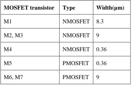
All the circuits have been designed in 0.18 µm TSMC CMOS technology. SPICE simulations have been performed at VDD = 1V and VBIAS = 0.35 V. The width parameters of various transistors are shown in Table 1.
Table 1 Width parameters for various MOSFET transistors
MOSFET transistor Type Width(µm)
M1 NMOSFET 8.3
M2, M3 NMOSFET 9
M4 NMOSFET 0.36
M5 PMOSFET 0.36
M6, M7 PMOSFET 9
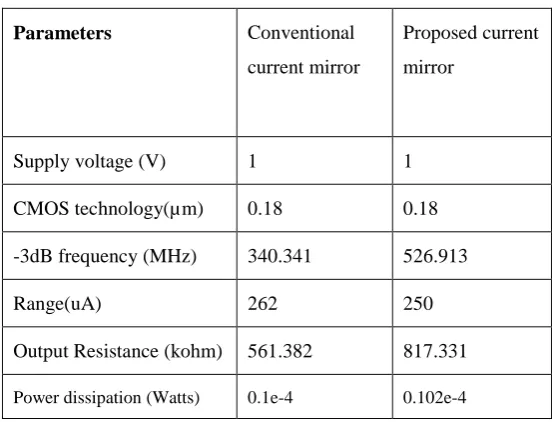
Fig.6 shows frequency response of conventional and proposed current mirror. -3dB frequency of CCM and PCM is obtained as 340.341 MHz and 526.913 MHz respectively. Thus bandwidth improves by a factor of 1.54 using biasing technique. Fig.7 shows transfer characteristics of CCM and PCM. The approximate range of PCM is 0-250 µA. Simulated output resistance of proposed current mirror is obtained as 817.331 kΩ and static power consumption is 102 µW.
1168 | P a g e
Fig.6 Bandwidth of PCMFig.7 Transfer characteristics of PCM
Input current(uA)
0 50 100 150 200 250 300
0 75 150 225 300
CCM PCM
O
u
tp
u
t
cu
rr
en
t(
u
A
)
Frequency(Hz)
10K 100K 1.0M 10M 100M 1.0G 10G -12
-9 -6 -3 0 3
Ga
in
(d
B)
1169 | P a g e
Fig.8 Step response of PCM.Most of the CM lie with the signal path of circuit therefore a CM having higher dynamic performance is desired for signal processing applications. Results of the PCM and CCM to a step change in input current from 25µA to 175 µA is shown in Fig. 8. From plotted graph, it can be observe that the step response of the PCM is faster than the CCM. The comparison between different parameters of proposed CM and conventional are shown below.
Table 2: Comparison of parameters of current mirrors
Parameters Conventional current mirror
Proposed current mirror
Supply voltage (V) 1 1
CMOS technology(µm) 0.18 0.18
-3dB frequency (MHz) 340.341 526.913
Range(uA) 262 250
Output Resistance (kohm) 561.382 817.331
Power dissipation (Watts) 0.1e-4 0.102e-4
V.CONCLUSION
The analog performance of nano scale devices are get damaged by ultra low voltage supplies embrace as per the technology is narrowing down, by the reduced gm/gds maximum achievable values. In this proposed work, the writers have disclosed a very new method of increasing the bandwidth of low voltage CMOS CM by means of a biasing technique via gate and bulk terminals. The distinctive feature of this biasing technique is that for bias
Time(ns)
0 1 2 3 4 5 6 7 8 9 10 11 12
0 25 50 100 125 150 175 200
C CM PCM Input
In
p
u
t(
µ
A
1170 | P a g e
voltage generation no extra circuitry is necessary. Approx. 187 MHz bandwidth of current mirror is get increased by our proposed work and output resistance by about 256 kΩ at low supply voltage of 1Volt. Analytical and simulation analysis shows the effectiveness of this approach. Given proposed technique does not put into effect on the DC current gain and supply voltage of original circuit and it is mainly attractive for low voltage CMOS current mirrors in high frequency applications. It is significant to mention that the improvements in bandwidth and resistance at output of the proposed CM have been achieved without compromising in silicon area and the huge power consumption.REFERENCES
[1] J. Ramírez-Angulo, R. G. Carvajal, A. Torralba, "Low supply voltage high performance CMOS current mirror with low input and output voltage requirements", IEEE Transactions on Circuits and Systems—II, Vol.51, No.3, 2004, pp.124-129.
[2] K. D. Peterson, L. G. Randall, "Area/bandwidth tradeoffs for CMOS current mirrors", IEEE Transactions on Circuits and Systems, Vol.CAS-33, No.1, 1986, pp.667-669.
[3] Peter R. Kinget, "Device Mismatch and Tradeoffs in the Design of Analog Circuits", IEEE Journal of Solid-State Circuits, Vol.40, No.6, 2005, pp.1212-1224.
[4] T. Voo, C. Toumazou, "High-speed current mirror resistive compensation technique", IEE Electronics Letters, Vol.31, No.4, 1995, pp. 248–250.
[5] T. Voo, C. Toumazou, "Precision temperature stabilized tunable CMOS current-mirror for filter applications", IEE Electronics Letters, Vol.32, No.2, 1996, pp.105–106.
[6] S. Bendong, F. Yuan, "A new inductor series-peaking technique for bandwidth enhancement of CMOS current-mode circuits", Analog Integrated Circuits and Signal Processing, Vol.37, 2003, pp.259–264. [7] F. Yuan, "Low Voltage CMOS current-mode circuits: topology and characteristics", IEE Proc-Circuits
Devices Systems, Vol.153, No.3,2006, pp.219-230.
[8] T. Itakura, T. Iida, "A feedforward technique with frequency dependent current mirrors for low-voltage wideband amplifier", IEEE Journal of Solid State Circuits, Vol.31, No.6, 1996, pp.847–850.
[9] N. Raj, A. K. Singh, A. K. Gupta, "Low voltage bulk driven self-biased cascode current mirror with bandwidth enhancement", IEE Electronics Letters, Vol.50, No.1, 2014, pp.23-25.
[10]P. E. Allen, D. R. Holberg, "CMOS analog circuit design", New York: Oxford University Press, 2003.
[11] S.S. Rajput, S.S. Jamuar, "A Current Mirror for Low Voltage, High Performance Analog Circuits" , Analog Integrated Circuits and Signal Processing,Vol.36, No.3, 2003, pp.221-233.
[12]M. Gupta, P. Aggarwal, P. Singh, N. K. Jindal, "Low voltage current mirrors with enhanced bandwidth",
1171 | P a g e
[13] P. Monsurrò, S. Pennisi, G. Scotti, "A. Trifiletti, Exploiting the body of MOS devices for highperformance analog design", IEEE Circuits and Systems Magazine, Fourth Quarter,2011,pp.8-23.
[14] V. Niranjan, M. Gupta, "Body biasing-a circuit level approach to reduce leakage in low power CMOS circuits", Journal of Active and Passive Electronic Devices, Vol.6, No.1-2, 2011, pp.89-99.
[15] F. Assaderaghi, D. Sinitsky, S. A. Parke, et. al., "Dynamic threshold voltage MOSFET for ultra low voltage VLSI", IEEE Transactions on Electron Devices, Vol.44, No.3, 1997, pp.414-422.
[16] P. R. Gray, P. J. Hurst, S. H. Lewis, R. G. Meyer, "Analysis and design of analog integrated circuits", Wiley Singapore, 2001.
[17] V. Niranjan, A. Kumar, S.B. Jain, "Triple well subthreshold CMOS logic using body bias technique",
IEEE International Conference on Signal Processing, Computing and Control, 2013, pp.1-6.