High Voltage Gain DC-DC Boost Converter
based Photovoltaic System Using Multilevel
Inverter fed Induction Motor
SUBUDDI SIVAKUMARM-tech Student Scholar
Department of Electrical & Electronics Engineering, Baba Institute of Technology;
Madhurawada,Visakhapatnam, A.P, India.
B.VENKATA RAMANA Associate Professor, HOD,
Department of Electrical & Electronics Engineering, Baba Institute of Technology;
Madhurawada,Visakhapatnam,A.P, India.
Abstract— Solar energy is the most low cost, competition free, universal source of energy as sun shines throughout. This energy can be converted into useful electrical energy using photovoltaic technology. The effective operation of Induction motor is based on the choice of suitable converter-inverter system that is fed to Induction Motor. Converters like Buck, Boost and Buck-Boost converters are popularly used for photovoltaic systems. This review is mainly focused on high efficiency step-up DC/DC converters with high voltage gain. To obtain optimum motor performance and to reduce total harmonic distortion of the inverter output waveform, we employed sinusoidal pulse width modulation (SPWM) technique based multilevel inverter for switching of inverter power circuit. In order to maximize the power output the system components of the photovoltaic system should be optimized. Maximum power point tracking algorithm (Perturb & Observe) is used to extract maximum power from photovoltaic panel. The proposed inverter can be replaced with multilevel inverter and is implemented MATLAB/SIMULATION software for better control of motor.
Index Terms— DC–DC Power Conversion, Capacitor Modules, Interleaved Methodology, PI Controller.
I.INTRODUCTION
Renewable-energy-based micro-grids have appeared to be a better way of exploiting renewable energy and reducing the environmental risks of fossil fuels. In the view of the fact that most renewable energy sources (RES), such as photovoltaic (PV), fuel cell (FC) and variable speed wind power systems, generate either DC or variable frequency/voltage AC power, a power–electronics interface is an indispensable element for the grid integration [1, 2]. In addition, modern electronic loads such as computers, plug-in hybrid electric vehicles and even traditional AC loads such as induction motors, when driven by a variables peed drive require DC power. The multilevel inverters have been considered as a key element in such grid-connected systems. Producing an acceptable sinusoidal voltage waveform at the output and boosting the output voltage are two challenging issues. Using a transformer in the boost multilevel inverter increases the size and cost and decreases the efficiency of the system
due to its bulky inductors. Multilevel Inverters (MLI) began with the neutral point clamped inverter topology proposed by Nabae et al. [3]. Recently, multilevel inverters have become more attractive for researchers due to their advantages over conventional three-level pulse width-modulated (PWM) inverters. MLI has two main advantages compared with the conventional H-bridge inverters, the higher voltage capability and the reduced harmonic content in the output waveform due to the multiple dc levels. MLI is now preferred in high power medium voltage applications due to the reduced voltage stresses on the devices.
The dc–dc boost converter can achieve a high step up voltage gain with an extremely high duty ratio. However, in practice, the step-up voltage gain is limited due to the effect of power switches, rectifier diodes, and the equivalent series resistance (ESR) of inductors and capacitors. Moreover, the extremely high duty-ratio operation will result in a serious reverse-recovery problem. A dc–dc fly back converter is a very simple structure with a high step-up voltage gain and an electrical isolation, but the active switch of this converter will suffer a high voltage stress due to the leakage inductance of the transformer. For recycling the energy of the leakage inductance and minimizing the voltage stress on the active switch, some energy-regeneration techniques have been proposed to clamp the voltage stress on the active switch and to recycle the leakage-inductance energy [4-6]. The coupled-inductor techniques provide solutions to achieve a high voltage gain, a low voltage stress on the active switch, and a high efficiency without the penalty of high duty ratio [7].
high power dissipation due to the leakage inductance of the transformer. Although this configuration is useful in terms of system monitoring and repair, the partial shading, module mismatch, and dc connection cable losses are inevitable problems and lead to significantly reduced system energy yields [8]–[10]. The ac module, which has been proposed to improve these problems, consists of a single PV panel and a micro-inverter. The micro-inverter receives the low dc voltage from the PV panel and transforms it to ac voltage, then delivers it to the load or main electricity as would a small scale conventional PV inverter.
Fig.1. General Configuration of inverter with Induction motor drive.
Fig.1 shows the energy of a single PV panel through the micro-inverter output to the main electricity; this is a general configuration of inverter with induction motor drive. The micro-inverter is inlaid in the rear bezel of the PV panel and outputs the ac current to the load or to the main electricity; this alternative solution not only immunizes the yield loss by shadow effect, but also provides flexible installation options according to the user’s budget [11]–[12]. Fig. 2 shows that the maximum power point (MPP) voltage range is from 15 V to 40 V with various power capacities of about 100 W to 300 W for a single commercial PV panel. When a wide input voltage range is essential for the single stage micro-inverter, high efficiency is difficult to achieve [13]. However, the dual-stage micro-inverter, which combines a high step-up dc/dc converter and dc/ac inverter, is able to achieve efficiency as high as the conventional PV string-type inverter [14]. Fig.1 also shows that the micro-inverter integrates a high step-up dc/dc converter and dc/ac inverter. The typical Zeta converter provides either a step-up or a step-down function to the output, in a manner similar to that of the buck-boost or SEPIC converter topologies. The conventional Zeta converter is configured of two inductors, a series capacitor and a diode
.
Fig. 2. Circuit Configuration of Proposed Converter.
However, leakage inductance issues that relate to the voltage spike and the efficiency remain significant. An integrated boost–fly back converter [15] based on a coupled inductor with high efficiency and high step-up voltage gain has been presented. The energy stored in the leakage inductor is recycled into the output during the switch off period. Thus, the efficiency can be increased and the voltage stress on the active switch can be suppressed. Many step-up converters, which use an output voltage stacking to increase the voltage gain, are presented.
II. PROPOSED CONVERTER TOPOLOGY
The simplified circuit model of the proposed converter is shown in Fig. 3. The coupled inductorT1 includes a
magnetizing inductor Lm, primary and secondary leakage inductors Lk1andLk2, and an ideal transformer primary
winding N1 and secondary winding N2. To simplify the
circuit analysis of the proposed converter, the following assumptions are made.
1) All components are ideal, except for the leakage inductance of coupled inductor T1.The ON-state resistance
RDS (ON) and all parasitic capacitances of the main switch S1are neglected, as are the forward voltage drops of
the diodesD1∼D3.
2) The capacitorsC1∼C3 are sufficiently large that the
voltages across them are considered to be constant. 3) The ESR of capacitorsC1∼C3and the parasitic resistance of coupled-inductorT1are neglected.
4) The turn’s ratio n of the coupled inductorT1winding is equal to N2/N1.
The operating principles for continuous-conduction mode (CCM) are now presented in detail. Fig. 4 shows the typical waveform of several major components during one switching period. The five operating modes are described as follows.
A. CCM Operation
Mode I[t0,t1]: In this transition interval, the secondary leakage inductor Lk2 is continuously releasing its energy to
as shown, switch S1and diodes D2are conducting. The
current iLm is descending because source voltage Vin is
applied on
Fig.3. Typical waveforms of the proposed converter at CCM operation.
magnetizing inductor Lm and primary leakage inductorLk1; meanwhile, Lm is also releasing its energy to
the secondary winding, as well as charging capacitorC2 along with the decrease in energy, the charging currentiD2andiC2are also decreasing. The secondary leakage inductor current iLK2 is declining according to
iLm/n. Once the increasing iLk1equals the decreasing iLm at
t=t1, this mode ends
(1)
(2)
(3)
(4) Mode II[t1,t2]: During this interval, source energy Vin is series connected withC1,C2, secondary winding N2, and Lk2 to charge output capacitor C3 and load R; meanwhile, magnetizing inductor Lm is also receiving energy from Vin. The current flow path is shown in Fig.4(b); as illustrated, switchS1 remains on, and only diodeD3is
conducting. The iLm, iLk1, andiD3are increasing because the
Vin is crossing Lk1,Lm and primary winding N1;Lm
andLk1are storing energy from Vin; meanwhile, Vin is also
in series with N2 of coupled inductor T1, and capacitors
C1andC2are discharging their energy to capacitor C3and
Fig.4. Current flow path in five operating modes during one switching period in CCM operation. (a) Mode I. (b) Mode II. (c) Mode III. (d)
Mode IV. (e) Mode V.
This mode ends when switch S1is turned off at t=t2
(5)
(6)
(7)
(8) Mode III [t2, t3]: During this transition interval, secondary leakage inductorLk2keeps chargingC3when switchS1is off. The current flow path is shown in Fig. 4(c), and only diodesD1 andD3are conducting. The energy stored in leakage inductor Lk1 flows through diodeD1 to
charge capacitor C1 instantly whenS1turns off. Meanwhile, the Lk2 keeps the same current direction as in
the prior mode and is in series withC2to charge output capacitorC3and load R. The voltage across S1is the summation of Vin, VLm, and VLk1. Currents iLk1andiLk2are
rapidly declining, but iLm is increasing because Lm is
receiving energy from Lk2. Once current iLk2 drops to zero,
this mode ends at t=t3
(9)
(10)
(11)
(12) Mode IV[t3,t4]: During this transition interval, the energy stored in magnetizing inductor Lm releases simultaneously to C1and C2. The current flow path is shown in Fig. 4(d).
Only diodes D1 and D2 are conducting. Currents iLk1 and
iD1 are persistently decreased because leakage energy still
flows through diode D1 and continues charging capacitorC1.The Lm is delivering its energy through T1
and D2 to charge capacitor C2. The energy stored in
capacitors C3is constantly discharged to the load R. The voltage across S1 is the same as previous mode. CurrentsiLk1 and iLm are decreasing, but iD2 is increasing.
This mode ends when current iLk1 is zero at t=t4
(13)
(14)
(15) Mode V[t4,t5]: During this interval, magnetizing inductor Lm is constantly transferring energy to C2. The current
flow path is shown in Fig. 5(e), and only diode D2 is
conducting. The iLm is decreasing due to the magnetizing
inductor energy flowing continuously through the coupled inductorT1to secondary winding N2 and D2 to charge
capacitorC2. The energy stored in capacitorsC3is constantly
discharged to the load R. The voltage acrossS1is the summation of Vin and VLm. This mode ends when
switchS1is turned on at the beginning of the next switching period
(16)
(17)
(18) III. MULTILEVEL INVERTER
Fig.5. Circuit diagram of five level inverter Here an auxiliary circuit consists of one switch and four diodes are used along with a full bridge configuration. The principle of operation of the proposed inverter is to generate five levels of output voltage, V/2, V, 0, -V/2 and –V. Using proper switching sequence in this modified circuit, five levels in output voltage is generated [10]. Table 1 shows the switching sequence used for generating five levels in the output voltage.
Table1: Switching sequence
IV. INDUCTION DRIVE
The ac power inverted by the multilevel inverter is fed to an induction drive. An induction or asynchronous motor is an AC electric motor in which the electric current in the rotor needed to produce torque is induced by electromagnetic induction from the magnetic field of the stator winding. An induction motor therefore does not require mechanical commutation, separate-excitation or self-excitation for all or part of the energy transferred from stator to rotor, as in universal, DC and large synchronous motors. An induction motor's rotor can be either wound type or squirrel-cage type. In induction, the AC power supplied to the motor's stator creates a magnetic field that rotates in time with the AC oscillations. The rotating magnetic flux induces currents in the windings of the rotor; in a manner similar to currents induced in a transformer's secondary windings. The currents in the rotor windings in turn create magnetic fields in the rotor that react against the stator field. Due to Lenz's Law, the direction of the magnetic field created will be such as to oppose the change in current through the rotor windings. The cause of induced current in the rotor windings is the rotating stator magnetic field, so to oppose the change in rotor-winding currents the rotor will start to rotate in the direction of the rotating stator magnetic field. The rotor accelerates until the magnitude of induced rotor current and torque balances
the applied load. Since rotation at synchronous speed would result in no induced rotor current, an induction motor always operates slower than synchronous speed. Under load, the speed drops and the slip increases enough to create sufficient torque to turn the load. An induction motor can be used as an induction generator, or it can be unrolled to form a linear induction motor which can directly generate linear motion.
V. MATLAB MODELEING AND SIMULATION RESULTS
Here the simulation is carried out by two cases, in that 1. Proposed DC/DC Converter. 2. Proposed DC/DC Converter with PV system and Induction motor.
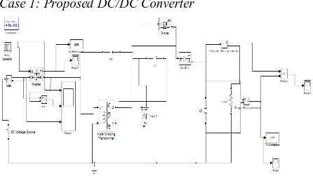
Case 1: Proposed DC/DC Converter
Fig.6. Matlab/Simulink Model of Proposed DC/DC Converter Operating Under Open Loop Condition
Fig.6. shows the Matlab/Simulink Model of Proposed DC/DC Converter Operating under Open Loop Condition using Matlab/Simulink Tool.
Fig.7. Output Voltage
Fig.8. Output Power
Fig.8. shows the Output Power of Proposed DC/DC Converter.
Fig.9. Switching States, Vds, Ids
Fig.9. shows the Switching States, Vds, Ids of Proposed DC/DC Converter Operating under Open Loop Condition.
Case 2: Proposed DC/DC Converter Operating with PV system and Induction motor.
Fig.10. Matlab/Simulink Model of Proposed DC/DC Converter Operating with PV system and induction motor.
Fig.10. shows the Matlab/Simulink Model of Proposed DC/DC Converter Operating with PV system and induction motor using Matlab/Simulink Tool.
Fig.11. inverter output voltage without filter.
Fig.11. shows the Output Voltage of five level inverter each phase output voltage without filter (a, b, c).
Fig.12.inverter voltage with filter.
Fig.12 shows the five level inverter output voltage with filter.
Fig.13.Simulation results for stator current, speed and electromagnetic torque of the motor.
VI. CONCLUSION
injury to humans or damage to facilities. Also this technique features easy implementation and more importantly, minimum harmonic content in the inverter output voltage and current of the Induction Motor Load. The simulation with multilevel converter with induction motor has been done and the output is verified.
REFERENCES
[1] Global Market Outlook for Photovoltaics Until 2014, Eur. Photovoltaic Ind. Assoc. (EPIA), Brussels, Belgium, May 2010. [Online]. Available:http://www.epia.org/fileadmin/EPIA_docs/public/Global_Mark et_ Outlook_for_Photovoltaics_until_2014.pdf
[2] T. Shimizu, K. Wada, and N. Nakamura, “Flyback-type single-phase utility interactive inverter with power pulsation decoupling on the dc input for an ac photovoltaic module system, ”IEEE Trans. Power Electron., vol. 21, no. 5, pp. 1264–1272, Jan. 2006.
[3] C. Rodriguez and G. A. J. Amaratunga, “Long-lifetime power inverter for photovoltaic ac modules, ”IEEE Trans. Ind. Electron., vol. 55, no. 7, pp. 2593–2601, Jul. 2008.
[4] W. Li and X. He, “Review of non-isolated high step-up dc/dc converters in photovoltaic grid-connected applications, ”IEEE Trans. Ind. Electron., vol. 58, no. 4, pp. 1239–1250, Apr. 2011.
[5] S. B. Kjaer, J. K. Pedersen, and F. Blaabjerg, “A review of single-phase grid-connected inverters for photovoltaic modules,”IEEE Trans. Ind. Appl., vol. 41, no. 5, pp. 1292–1306, Sep./Oct. 2005.
[6] B. Jablonska, A. L. Kooijman-van Dijk, H. F. Kaan, M. van Leeuwen, G. T. M. de Boer, and H. H. C. de Moor, “PV-prive project at ECN, five years of experience with small-scale ac module PV systems,” inProc. 20th Eur. Photovoltaic Sol. Energy Conf., Barcelona, Spain, Jun. 2005, pp. 2728–2731.
[7] J. J. Bzura, “The ac module: An overview and update on self-contained modular PV systems,” inProc. IEEE Power Eng. Soc. Gen. Meeting, Jul. 2010, pp. 1–3.
[8] J. Falin, “Designing dc/dc converters based on ZETA topology,” Analog Appl. J., pp. 16–21, 2Q, 2010. [Online]. Available: http://focus.ti. com/lit/an/slyt372/slyt372.pdf
[9] B. R. Lin and F. Y. Hsieh, “Soft-switching Zeta-flyback converter with a buck-boost type of active clamp,”IEEE Trans. Ind. Electron., vol. 54, no. 5, pp. 2813–2822, Oct. 2007.
[10] T. B. Marchesan, M. A. Dalla-Costa, J. M. Alonso, and R. N. do Prado, “Integrated Zeta-flyback electronic ballast to supply high-intensity discharge lamps,”IEEE Trans. Ind. Electron., vol. 54, no. 5, pp. 2918– 2921, Oct. 2007.
[11] D. Murthy-Bellur and M. K. Kazimierczuk, “Two-transistor Zeta-flyback dc-dc converter with reduced transistor voltage stress,”Electron. Lett., vol. 46, no. 10, pp. 719–720, May 2010.
[12] T. F. Wu, S. A. Liang, and Y. M. Chen, “Design optimization for asymmetrical ZVS PWM Zeta converter,”IEEE Trans. Aerosp. Electron. Syst., vol. 39, no. 2, pp. 521–532, Apr. 2003.
[13] M. J. Bonato, F. T. Wakabayashi, and C. A. Canesin, “A novel voltage step-down/up ZCS-PWM Zeta converter,” inConf. Rec. IEEE IAS Annu. Meeting, 2000, pp. 2448–2454.
[14] B. Axelrod, Y. Berkovich, S. Tapuchi, and A. Ioinovici, “Steep conversion ration ´ Cuk, Zeta, and sepic converters based on a switched coupled-inductor cell,” inProc. IEEE Power Electron. Spec. Conf., 2008, pp. 3009–3014.