I
PROGRAMMEF~
REFEREN
PROCESSOR
AND
STORAGE
This document contains the latest information available at the time of publication. However, the Univac Division reserves the right to modify or revise its contents. To ensure that you have the most recen~ information, contact your local Univac Representative.
UN IVAC is a registered trademark of the Sperry Rand Corporation.
UP-7546 Rev. 1 UP.NUMBER
Section
-Cover/Disclaimer
PSS
Contents 1
2 3
Appendix A
-Appendix B
Appendix C Appendix D
Index
Page
Number
1 1 thru 5
1 thru 17 1 thru 34 1 thru 21
1 thru 3
1 thru 3 1 thru 4 1
1 thru 11
Update
Level
UNIVAC 9200/920011/9300/9300 II
PROCESSOR AND STORAGE
PAGE STATUS SUMMARY
ISSUE:
UP-7546 Rev. 1
Section
Page
Number
Update
Level
PSS-l PAGE REVISION PAGE
Section
Page
Number
UP-7546 Rev. 1
UNIVAC 9200/9200 11/9300/9300 II PROCESSOR AND STORAGE
PAGE STATUS SUMMARY
CONTENTS
1. INTRODUCTION
1.1.
GENERAL1.2.
SYSTEM CONFIGURATION 1.1, COMPONENT DESCRIPTION1.3,,1.
Processor1.3.1.1.
Main Storage1.3.1.2.
Control1.3.1.3.
Arithmetic1.3.1.3.1.
Multiply, Divide, and Edit1.3.,1.3.2.
Subtraction by Two's Complement Method1.3.1.4.
Input/Output1.3.1.4.1.
Multiplexer Channel1.3,,1.4.2.
Selector Channel1.3.,2.
Printer1.
3 ..2.1. 300
L PM P ri nt Speed1.3.2.2. 120
Print Positions1.3.2.3.
Print Position Expansion1.3.2.4. 132
Print Positions1.3.2.5.
Variable Speed Printing1.3.2.6. 8
LPI Print Spacing1.3.2.7.
Form Alignment1.3.2.8.
High Speed Numeric Print 1.4. DATA FORMATS AND CODES 1.4.1. Binary Number Representation1.4.2.
Hexadecimal Representation1.4.3.
Decimal Number Representation1.4.3.1.
Sign Bits1.4.4.
Character Representation1.4.5.
Parity Verification 1.4.6. OP Codes1.4.7.
Logical InformationContents SEC TION:
CONTENTS
1-1
1-4
1-9 1-9 1-9 1-9 1-9 1-9 1-101-11
1-11
1-12
1-121-12
1-13
1-13
1-131-13
1-13
1-13
1-13
1-141-15
1-15
1-161-16
1-17
1-17
1-17
1-17
1
UP-7546
Rev. 1
UNIVAC 9200/9200 11/9300/9300 II
PROCESSOR AND STORAGE
2. PROCESSOR UNIT
2.1.
MAIN STORAGE2.1.1.
Privileged and Low Order Storage2.1.2.
Storage Boundaries2.1.3.
Parity Checking2.1.4.
Interrupts2.2.
PROCESSOR CONTROL2.2.1.
Program State Control2.2.1.1.
Processor Program State Control Words (Bytes0-3)
2.2.1.2.
Input/Output Program State Control Word (Bytes16-19)
2.2.2.
Restricted Alter/Display and Operator Request (Bytes4,5)
2.2.3.
Machine Instruction Register (Bytes6-11)
2.2.4.
Restart Instruction Register (Bytes22-25)
2.2.5.
Spec i al Statu s (Bytes29-31)
2.2.6.
Processor Program Register (Bytes32-47)
and Input/Output Program Registers (Bytes48-63)
2.2.7.
Device Status (Byte66)
and Device Address (Byte67)
2.2.8.
Buffer Control Words (Bytes68-127)
2.2.8.1.
Multiplexer Subchannel BCW2.2.8.2.
Device Control Subchannel Numbering2.2.8.3.
Buffer Control Word Location2.2.8.4.
Additional Nonshared Subchannel Device Addresses2.2.9.
Printer Image Area (Bytes128-259)
2.2.10.
Printer Control2.2.10.1.
P ri nter Instru ctions2.2.10.2.
Printer Buffer Control Word2.2.10.3.
Issue and Execute2.2.10.4.
status Register2.2.10.5.
Interrupt Requests2.2.10.6.
Printer Status Byte2.2.11.
Input/Output Control2.2.12.
Operator-Ini tiated Functions2.2.12.1.
Load Cycle2.2.12.2.
Alternate Execute and Staticize Cycle2.3.
MUL TIPLEXER CHANNEL CONTROL2.3.1.
Multiplexer Channel Instructions2.3.2.
Multiplexer Channel Buffer Control Word2.3.3.
Multiplexer Channel Status Byte2.3.4.
Condition Code2.3.5.
Alternate BCW Format2.3.5.1.
Data Di rection Control2.3.6.
Polling2.3.6.1.
Priority of Interrupt2.3.7.
Special Channel Instructions and Interrupts2.3.7.1.
Operator Interrupt2.3.7.2.
Alternate (L T) Summary Interrupt2.3.7.3.
One-Second Interrupt2.3.7.4.
Summary of Special Channel Instructions2.3.8.
Channel Checking2.3.8.1.
Interface Error FI ip-Flop2.3.8.2.
Device Address Parity2.3.8.3.
Parity Error Flip-FlopContents SECTION:
2-1
2-1
2-2
2-3
2-3
2-4
2-6
2-6
2-7
2-7
2-7
2-8
2-8
2-8
2-8
2-8
2-9
2-9
2-9
2-9
2-10
2-10
2-10
2-10
2-11
2-12
2-12
2-13
2-13
2-14
2-15
2-15
2-15
2-15
2-16
2-16
2-17
2-17
2-18
2-19
2-19
2-20
2-20
2-20
2-21
2-21
2-21
2-22
2-22
2-22
2-22
2
UP-7546 Rev. 1
UNIVAC 9200/9200 11/9300/9300 II
PROCESSOR AND STORAGE
2.4. SELECTOR CHANNEL CONTROL 2.4.1. Channel Addressing
2.4.1.1. Selector Channel Address Format 2.4.1.2. Mu Itip lexer Channel Address Format 2.4.2. Processor Lock-Out
2.4.3. Concurrent Operations 2.4.4. Command Chaining
2.4.!J. Execute I/O and Test I/O Instructions 2.4.6. I/O Commands
2.4.7. Transfer-in-Channel (TIC) Command 2.4.8. Condition Code (CC)
2.4.9. Channel Address Word (CAW) and Diagnostic Interrupt 2.4.10. Channel Command Word (CCW)
2.4.11. Device Status
2.4.12. Channel Status Word (CSW) 2.4.13. Channel Check i ng
2.4.14. Special Selector Channel Instructions
2.5. DATA TRANSLATION
2.5.1. Card Code Translation (SO-Column Card) 2.5.1.1. Card Code Image Mode (SO-Column Card) 2.5.2. Card Code Translation (90-Column Card) 2.5,2.1. Card Code Image Mode (90-Column Card) 2.5.3. Internal Codes
3. INSTRUCTIONS
3.1. GENERAL
3.2. INSTRUCTION FORMAT
3.2.1. Register and Indexed Storage Operation (RX) 3.2.2. Storage and Immediate Operand Operation (SI) 3.2.3. Storage-to-Storage (SS1)
3.2.4. Storage-to-Storage (SS2)
3.3. INSTRUCTION REPERTOIRE 3.3.1. Binary Instructions and Overflow 3.3.1..1. Store Halfword Instruction (STH) 3.3.1.2. Load Halfword Instruction (LH) 3.3.1.3. Compare Halfword Instruction (CH) 3.3.1.4. Add Immediate Instruction (AI) 3.3.1.5. Add Halfword Instruction (AH) 3.3.1.6. Subtract Halfword Instruction (SH) 3.3.2. Logical Instructions
3.3.2.1. Test Under Mask Instruction (TM) 3.3.2.2. Move Immediate Instructions (MVI) 3.3.2.3. AND Immediate Instruction (NI)
3.3.2.4. Compare Logical Immediate Instruction (CLI) 3.3.2.5. OR Immediate Instruction (01)
3.3.2.6. Halt and Proceed Instruction (HPR) 3.3.2.7. Move Numeric Instruction (MVN) 3.3.2.S. Move Character Instruction (MVC) 3.3.2.9. AND Character Instruction (NC)
3.3.2.10. Compare Logical Character Instruction (CLC) 3.3.2.11. 0 R Character Instructi on (0 C)
Rev. 1
UNIVAC 9200/9200 11/9300/9300 II
PROCESSOR AND STORAGE SECTION: Contents
4
PAGE:U P - 7 5 4 6 L
---~~---~---~---3.3.2.12.
Translate Instruction (TR)3.3.2.13.
Edit Instruction (ED)3.3.3.
Decimal Instructions3.3.3.1.
Move with Offset Instruction (MVO)3.3.3.2.
Pack Instruction (PACK)3.3.3.3.
Unpack Instruction (U N PK)3.3.3.4.
Zero Add (Packed) Decimal Instruction (ZAP)3.3.3.5.
Compare (Packed) Decimal Instruction (CP)3.3.3.6.
ADD (Packed) Decimal Instruction (AP)3.3.3.7.
Subtract (Packed) Decimal Instruction (SP)3.3.3.8.
Multiply (Packed) Decimal Instruction (MP)3.3.3.9.
Divide (Packed) Decimal Instruction (DP)3.3.4.
Bran ch I nstructi on s3.3.4.1.
Branch-on-Condition Instruction (BC)3.3.4.2.
Branch and Link Instruction (BAL)3.3.5.
State Control (Privileged and Special) Instructions3.3.5.1.
Load Program State Control Instruction (LPSC)3.3.5.2.
Store Program State Control Instruction (SPSC)3.3.5.3.
Supervisor Request Call Instruction (SRC)3.3.6.
Input/Output Instruction3.3.6.1.
Execute I/O Instruction (XIO F)3.3.6.2.
Test I/O Instruction (TID)APPENDIXES
A, INSTRUCTIONS, FORMATS, CODES
B. HEXADECIMAL TABLES
C. CHARACTER GRAPHIC SET CODES AND PRINTER SYNCHRONIZER CODE
D. POWERS OF 2; POWERS OF 16
INDEX
TABLES
1-1.
Configurations for UNIVAC9200
and9300
Systems Processors1-2.
Hexadecimal-Decimal Conversion3-1.
Instruction Mnemonics in Alphabetical Sequence3-2.
Instructions Grouped by Functional Type3-3.
Instructions Grouped by Format3-4.
Instructions in Sequence of Hexadecimal Codes3-12
3-12
3-13
3-13
3-14
3-15
3-15
3-15
3-15
3-16
3-16
3-18
3-20
3-20
3-20
3-20
3-20
3-21
3-21
3-21
3-21
3-21
1-4
1-15
3-2
3-3
3-4
UP-7546 Rev. 1
FIGURES
1--1.
1-- 2.
1-3.
1--4.
1-5.
1--6.
2-1.
2--2.
2--3.
2--4.
2 --5.
2--6.
3--1.
UNIVAC 9200/9200 11/9300/9300 II
PROCESSOR AND STORAGE
UNIVAC 9200/9200 11/9300/9300 II Systems Processor
UN I V AC 9200/9200 11/9300/9300 II Systems Processor Block 0 iagram
Configuration for UNIVAC 9200 System Processor
Configuration for UNIVAC 9200 II System Processor
Configuration for UNIVAC 9300 System Processor
Configuration for UNIVAC 9300 II System Pr,ocessor
M a i n Slo rag e 0 r g ani z a t ion
Organization of First 260 Bytes of Storage
Compressed Code for 80-Column Card
Image Mode for 80-Column Card
Card Code Tran.slation for 90-Column Card
Image Mode for 90-Column Card
Instruction Formats
Contents 5
SECTION: P AG E:
1-1
1-2
1-5
1-6
1-7
1-8
2-2
2-5
2-32
2-33
2-33
2-34
UP-7546 Rev. 1
UNIVAC 9200/9200 11/9300/9300 II
I
1I
_ _ _ _
P_R_O_C_E_SS_O_R_A_N_D_S_T_O_R_A_G_E
_ _ _ _ _
~
_ _ _ _
~~.~~
1. INTRODUCTION
Figure 1-1. UNIVAC 9200/9200 1//9300/9300 /I Systems Processor
1.1. GENERAL
This document contains a description of the UNIV AC 9200/9200 11/9300/9300 II Systems processor with optional features pertaining to expans ion, internal operation of the processor, data and program information presentation, instruction repertoire and coding, and constant and s1torage definitions.
It should be noted that only one processor is detailed herein with the specific differences between each noted as required. The four system processors are identic all in appearance. The configuration is shown in Figure 1-1.
This manual is divided into the following basic sections:
• Introduction
• Processor Unit
• Instructions
• Appendix
Upa'7546
Rev. 1
L
1UNIVAC 9200/9200 11/9300/9300 II
PROCESSOR AND STORAGE SECTION: PAGE:
The UNIV AC 9200/9200 11/9300/9300 II Systems processor shown in Figure 1--1, is a byte-oriented data processor integrated with an attached printer and an optional externally-connected card punch and card reader (basic peripherals). A wide range of other peripheral devices may be incorporated either initially by replacing one or more of these basic peripheral devices, or later, by adding to the system.
Two major functions of the processor are decoding and storage. The decoding func-tion analyzes each instrucfunc-tion to determine required operafunc-tions and the locafunc-tion of needed information. An instruction containing labels of data in storage is decoded to find the addresses and lengths of the operands (data to be processed), as well as the particular operation that is to be performed on the data. The processor then re-sponds to the instruction by using generated control signals. The storage (memory) portion of the processor stores the data and instructions required by the program in addressable locations that are easily accessible to the program.
The major components of the UNIV AC 9200/9200 11/9300/9300 II Systems processor are shown in Figure 1-2.
CONTROL TO I/O DEVICE DATA AND
STATUS FROM I/O
DEV ICE
~
.
...---r---,
I
STORAGE PLATED: ADRI
I
UNIT WIRE I S. I STORAGE~
ADDR ESSI
~ STORAGE I REG.BUFFER
r- - - ' - - - -
I
I
STOR. DATA REG. I (MA)L_ -
~--1--
:....J
INTERNAL INPUT
DATA STORAG E
OUTPUT AND
~ REGISTER r-O+- ADRS.REG. MULTIPLEXER ~
CHANNEL (D REG) (MAREG)
SYNCHRONIZERS
~
TEMPORARY
FUNCTION DATA STORAGE
....
REGISTER REG_
(F REG) (D REG)
~
l
ADDER FUNCTION
INPUT NETWORK
r+-
DECODE(ACX) TABLE
~
---y
~
ADDER AND SEQUENCE
-
PARITY COUNTER AGENERATOR (SA CTR)
~
SEQUENCE
-
COUNTER B (SB CTR)Figure 1-2. UNIVAC 9200/9200 1//9300/9300 /I Systems
Processor Block Diogrom
-CONTROL TO ALL COMPONENT
f
~ FUNCTIONCONTROL FF'S ~ AND GATING
S
UP-7546 Rev. 1
UNIVAC 9200/9200 11/9300/9300 II
I
11
-, ________
P_R_O
__
C_E_S_S_O_R __ A_N
__
D_S_T
__
O_R_A_G
__
E
__________
~
___________
~~~~
They are controlled and coordinated by means of internally stored programs which are derived from a standard instruction repertoire. The function of each of the com po-nents is as follows:
• Storage Unit - Comprises registers used in the processing and storage of all instructions and data that is to be, or has been, processed.
• Data Register (D Reg)
•
Temporary Data Storage Register (B Reg)•
Adder Input Network (ACX)•
Adder and Parity GeneratorProvides temporary storage for data that is currently being processed. All tran sfer of data between the proc essor or peripheral units and the storage unit is accomplished through the data register.
Provides additional temporary storage for data currently being processed, an d also for various special codes required for process control and addressing.
- Gates, modifies, and generates data involved in processing program data or special control codes.
- Performs various processes specified by the instructions, such as addition, subtraction, and the formation of AN D- and OR- products. Also generates parity.
• Storage (Memory) - Addresses of data being processed. Address Buffer
(MA)
• Storage (Memory) - Stores the addresses of data currently being processed. Address Register
(MA Reg)
• Function Register - Stores the partial decoded function code specified in an (F Reg) instruction.
• Function Decode Table
• Sequence Counters A and B (SA CTR, SB CTR)
• Function Control Flip-flops and Gating
- Interprets instructions and generates the control signals required for the initiation of the required process.
- Controls sequencing of the various control signals required to complete a process specified by an instruction. Although outputs of both counters control the generating of funct,ion signals, sequence counter A is used as a first-stage input to the second-stage sequence counter B.
U P - 7 5 4 6 L Rev. 1
---
-UNIVAC 9200/9200 11/9300/9300 II PROCESSOR AND STORAGE
1.2. SYSTEM CONFIGURATION
The UNIVAC 9200/9200 11/9300/9300 II Systems processor is housed in two separate cabinets. The larger of the two cabinets con tains an operator's control panel, a printer, and the integrated logic circuit packages. The second cabinet is the elec-tronics cabinet; it contains the storage (memory) circuitry and the power supplies and power distribution panel for the entire processor.
Table 1-1 lists the basic and optional processor equipment for each of the four systems (UNIV AC 9200, 9200 II, 9300, 9300 II). Figures 1-3, 1-4, 1-5, and 1-6 illustrate the system configurations for these systems.
UNIVAC SYSTEMS 9200 9200 II
Printer Processor Printer Processor o Control
o Printer
o Form control loop o 250 lPM bar printer
96 print positions 63 char acter pr int bar o ElK-byte storage
Expandab Ie to 16K byte
1.2 Ilsec. cycle time
o J~rithmeticControl
Control for printer, punch, and reader Multiplexer channel; accesses up to 8 sub-5,ystems or another processor
Multiply, divide, edit s
2;00 lPM print speed 120 print pOSitions Print position expansio 132 print pOSitions Variable speed printing 8 lPI print spacing Form a I ignment
n -LEGEND: 0 0 0 0 0 0 0 * * t I t t t r t
o Basic Equipment
Control Printer
Form control loop 250 lPM bar printer 96 print positions 63 character print bar 8K-byte storage Expandab Ie to 32K bytes
1.2 Ilsec. cycle time
Ar It hmet icC ontro I Control for printer, punch, and reader Multiplexer channel; accesses up to 8 sub-systems or another processor
Multiply, divide, edit Se lector c hanne I 300 lPM print speed 120 print pOSitions Print pOSition expansion 132 print pOSitions Variable speed printing 8lPI print spacing Form alignment
*
Processor Optional Features Printer Optional FeaturesPROCESSORS
9300 9300 II Printer Processor Printer Processor
0 Control 0 Control
0 Printer 0 Printer
0 Form control loop 0 Form control loop
0 600 lPM bar printer 0 600 lPM bar printer 120 print pOSitions 120 print pOSitions 63 character print bar 63 character print bar
0 8K-byte storage 0 16K-byte storage Expandab Ie to 32K bytes EXpandable to 32K bytes
0.6Ilsec. cycle time 0.6 Iisec. cycle time
0 Ar ithmetic Control 0 Ar it hmet ic /C ontro I Control for printer, Control for printer, punch, and reader punch, and reader
* Multiplexer channel; 0 Multiplexer channel; accesses up to 8 sub- accesses up to 8 sub-s ysub-s te msub-s or another systems or another processor processor
0 Multiply, d iv ide, ed it 0 Multiply, divide, edit
0 Se lec tor c hanne I
t Print position expansion t Print position expansion I High speed numeric print t High speed numeric print I 8 lPI print spacing r 8 lPI print spacing
Table 7-7. Configurations for UNIVAC 9200 and 9300 Systems Processors
UP-7546 Rev. 1
UNIVAC 9200/9200 11/9300/9300 II PROCESSOR AND STORAGE
,---~---
~--UNIVAC 9200 SYSTEM PROCESSOR
9200 PR OC ESS OR 3030-00
PR INTER AND PH INTER CONTROL 250 LF'M
96 PRINT POSITIONS 63··CHARACTER PRINT BAR
FOfIMS CONTROL LOOP
LEGEND:
C==J
BASIC EQUIPMENT CARD READER. CONTROLCARD
, - MULTIPLY;--D IVI MULTIPLY;--DE/
EDIT F0882-00 MUL TIPLEXER
I I/O CHANNEL
I
L __
~8~-~_1- - -: PROCESSOR OPTIONAL FEATURES !.._-_.'
PRINTER OPTIONAL FEATURES
NOTIE: ALL HARDWARE AND FEATURE NUMBERS SHOWN APPLY TO EQUIPMENT FOR 60Hz OPERATION. COUNTERPARTS ARE AVAILABLE FOR 50Hz OPERATION.
I I
---l
NDOR
8K BYTE STORAGE 1.2 pSEC
---.,.----,
I I
4 K. B YT E 14K B VT E I STORAGE: STORAGE I EXPANSION I EXPANSIONI
1.2pSEC I l.2pSEC :
I
I
: I 1.--_7_00_7_-9_3---1_
~~8':'0::8_L! ~:~::7J
r---, - -- - --,
12K BYTE STORAGE 1.2pSEC
I I
4K BYTE I
STORAGE I
EXPANSION I . I 1.2 pSEC I I
I
I
,--_7_00_7_-9_2~_ ~1~0'::6J
OR 16K BYTE STORAGE 1.2 pSEC
7007-91
UP-7S46~
Rev. 1
-UNIVAC 9200/9200 11/9300/9300 "
PROCESSOR AND STORAGE
SECTION: 1UNIVAC 9200 II SYSTEM PROCESSOR
_ . _
-9200 II PR OC ESSOR 3030-94
8K B YT E STORAGE 1.2 flSEC
- - - - 1 - - - - ,
I
14K BYTE 4K BYTE
I
I-AND
,...--STORAGE I ,...--STORAGE I EXPANSION: EXPANSION I 1.2 fl SEC I 1.211SEC
I
---~---~
PR INTER AND PRINTER CONTROL
LEGEND:
c=J
BASIC EQUIPMENT CARD READER.CONTROL
r---
I MULTIPLY / DIVIDE,' : EDIT I F0882-00MUL TIPLEXER I/O C HANNE L
SELECTOR CHANNEL DUAL I/O C HANNE L
F1104-99 I
~---______ I
:
____ J
PROCESSOR OPTIONAL FEATURESC::J
PRINTER OPTIONAL FEATURESNOTE: ALL HARDWARE AND FEATURE NUMBERS SHOWN APPLY TO EQUIPMENT FOR 60Hz OPERATION. COUNTERPARTS ARE AVAILABLE FOR 50Hz OPERATION.
OR
OR
FIRST 1 SECOND 1
EXPANSION IEXPANSION
I
I
I
,-_70_0_7-_93---,
!~9~9~ LF~890-:':
J
12K BYTE STORAGE
1.2 flSEC
----r---l
4K BYTE 116K BYTE 1
STORAGE I STORAGE I EXPANSION I EXPANSION I
1.2 flSEC 1 1.2 fl SEC
I
I I
FIRST I SECOND
I
EXPANSION IEXPANSIONI
: I '--_70_0_7-_92----J~0890-96_1~0890-9~
16K BYT E STORAGE 1.2 flSEC
---,
16K BYTE II
STORAGE EXPANSION
I
-
1.2 flSEC :OR
OR
I
I
L--7_0_0_7 -_9_1 - ' ._F
~90-~
J
- - I
24K BYTE 8K BYTE
I
STORAGE STORAGEI
1.2 flSEC EXPANSIONI
1.2 flSECI
I
I
I
7007-87 F0890-93I
L--_ _ ---' _ _ _ _ .J32K BYTE STORAGE 1.2 flSEC
7007-85
UP-7546
Rev. 1
UNIVAC 9200/9200 11/9300/9300 II PROCESSOR AND STORAGE
,---~---
~~-.
UNIVAC 9300 SYSTEM PROCESSOR
PR INTER AND PRINTER CONTROL
9300 PROCESSOR 3030-02
CARD READER. CONTROL 600 LPN!
120 PRINT POSITIONS CARD 63-CHA,R,A.CTER PRINT BARS • PUNCH
FORMS CONTROL LOOP CONTROL
MULTIPLY/ DIVIDE/ EDIT
~---~---~
LEGEND:
C]
BASIC EQUIPMENT[==~~~~ PROCESSOR OPTIONAL FEATURES PRINTER OPTIONAL FEATURES
MULTIPLEXER I/O CHANNEL
NOTE: ALL HARDWARE AND FEATURE NUMBERS SHOWN APPLY TO EQUIPMENT FOR 60Hz OPERATION. COUNTERPARTS ARE AVAILABLE FOR 50Hz OPERATION.
OR
OR
OR
OR
8K BYTE STORAGE
0.6/lSEC
----r----l
4K BYTE' 4K BYTE I STORAGE
I
STORAGE IEXPANSION
I
EXPANSION I 0.6/lSECI
0.6/lSECI
FIRSTI
SECOND : EXPANSION: EXPANSIONI
L..-_700_7_-08_.J~ ~9~0:"
L
F~8~-~
J
12K BYTESTORAG E 0.6/lSEC
7007-10
---r- - - -
r - - - l
4K BYTE I 8K BYTE
I
8K BYTE I STORAGE I STORAGE1 STORAGEI
EXPANSIONI
EXPANSION I EXPANSIONI
0:6/lSECI
0.6/lSEC I 0.6/lSEC II
FIRST
I
SECOND I THIRDI
EXPANSIONI
EXPANSIONI
EXPANSIONI
I I
I
F0890-92
I
F0890-05I
F0890-06I
L..-_ _ - - ' _ - - - , - - - - -- - - - 7
16K BYTE STORAGE 0.6/lSEC
- - - - 1
16K BYTE
I
STORAGEI
EXPANSIONI
0.6/lSECI
I
I
I
L..-7_0_07_-_12--, ~ ~~~J
24K BYTE STORAGE 0.6/lSEC
----l
8K BYTEI
STORAGEI
EXPANSION0.6/lSEC
I
I
I
I
L-_70_0_7-_18-.J ~ O~~:J32K BYTE STORAGE
0.6/lSEC
7007-14
"
" OR /"
'r----(
I 16K BYTE. I I STORAGE
I
I
EXPANSION II
0.6/lSEC II
SECOND II
EXPANSION II
I
I
L. ____ F0890-02 .J IUP-7S46~
Rev. 1
---UNIVAC 9200/9200 11/9300/9300 II
PROCESSOR AND STORAGE SECTION: 1
UNIVAC 9300 II SYSTEM PROCESSOR
9300 1\ PROCESSOR 3030-96
~---~C~A=RD~~
PRINTER AND PRINT CONTROL 600 LPM
READER. CONTROL
120 PRINT POSITIONS CARD 63-CHARACTER PRINT BAR ·PUNCH FORMS CONTROL LOOP CONTROL
LEGEND:
c=J
BASIC EQU IPMENT::=.-_-_-_-j
PR OCESSOR OPT 10NA L FEAT URESg~"~:J PRINTER OPTIONAL FEATURES
MULTIPLY/ DIV IDE/
EDIT
MU L TIPLEXER I/O C HANNE L
SELECTOR CHANNE L
NOTE: ALL HARDWARE AND FEATURE NUMBERS SHOWN APPLY TO EQUIPMENT FOR 60Hz OPERAT ION. COUNTERPARTS ARE AVAILABLE FOR 50Hz OPERAT ION.
AND
OR
OR
16K BYTE STORAGE 0.6I1 SEC
----1---,
SK BYTE I SK BYTE I STORAG E STORAGE EXPANSIONI EXPANSIONI
0.6 I1SEC
I
0.6I1SECI
FIRST I, SECOND I EXPANSION EXPANSIONI
I
I
,--_70_0_7_-1_2--l..!:.OS90-05
J.
~~o~~
...
'bR
\
24K BYTE STORAGE 0.6I1 SEC
...
"
\---lr-~--1
SKBYTE I I 16KBYTEI STORAGE I I STORAGEI
EXPANSION ' I EXPANSION I0.6I1SEC I I 0.6I1SEC I
1\
I
II
I
L . - -7_O_O_7 -_1S _____ F
OS9~0:J
L
~~~~J
32K BYTE STORAGE
0.6 I1SEC
7007-14
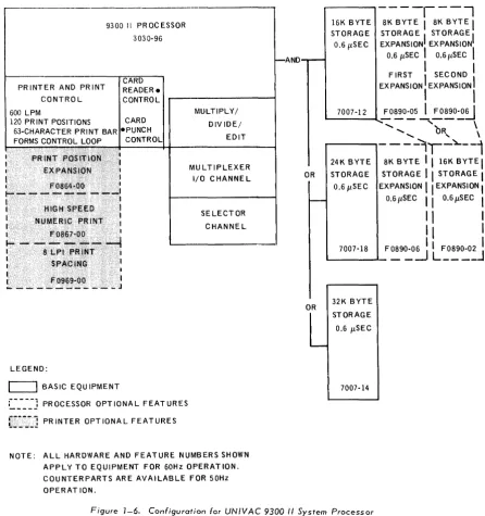
Figure 1-6. Configuration for UNIVAC 9300 /I System Processor
UP-7546 Rev. 1
UNIVAC 9200/9200 11/9300/9300 II
I
1I
9~~~_P_R_O_C_E_S_S_O_R_A_N_D~S_T_O_R_A_G_E~~~~~~~~~~~~~_~_
1.3. COMPONENT DESCRIPTION
Components for the different systems are generally rather similar. For this reason, the descriptions which follow apply, with exceptions noted, regardless of the system in which the component is used.
1.3.1. Processor
The major portions of the UNIVAC 9200/9200 11/9300/9300 II Systems processor are the main storage, control, arithmetic, and input and output.
1.3.1.1. Main Storage
The main storage portions of the processor is a separate free standing unit connected to the printer processor cabinet. The storage elements are of the plated wire, cylin-drical thin film type. The storage unit operates either in a read, write, or lockout mode at a cycle rate of 1.2 microseconds for the UNIVAC 9200 and 9200 II Systems pro-cessor; and at a rate of 0.6 microseconds for the UNIVAC 9300 and 9300 II Systems processor. Reading is nondestructive; that is, the data is not erased from storage by the read process.
The main storage is used to hold data received from input peripherals, results of processing, data to be distributed to output peripherals, programmed instructions, and control information.
The minimum basic storage is 8,192 bytes of nine bits each (eight data bits and one parity bit), except that the UNIVAC 9300 II Systems processor has a minimum of 16,384 bytes. The basic storage units may be expanded to 12,288, 16,384, 24,576, or 32,768 bytes except for the UNIVAC 9200 Systems processor, which is limited to 16,384 bytes.
1.3.1.2. Control
The control portion of the processor controls the sequence, interpretation, and execution of each instruction. The cycling of main storage is initiated by this section. All of the hardware aspects of interrupt handling, error checking, and protection are performed by the con trol section. The control section maintains the program address location counter and provides for the different processor modes of operation.
1.3.1.3. Arithmetic
The arithmetic portion of the processor performs data manipulations includ :ing binary and decimal arithmetic operations, and logical operations. The basic UNIVAC 9200 and 9200 II Systems processor is limited to machine addition only. Subtraction is performed by converting the subtrahend to its two's complement and adding. To multiply and divide, a suitable subroutine must be inserted into the user's program. The Multiply, Divide, and Edit capability (see 1.3.1.3.1) is available as an option.
1.3.1.3.1. Multiply, Divide, and Edit
UP-7546
I
Rev.1 ~
UNIVAC 9200/9200 11/9300/9300 II
PROCESSOR AND STORAGE
SECTION: 1 PAGE:1.3.1.3.2. Subtraction by Two's Complement Method
Because the fundamental arithmetic operation of the processor is addition, to perform subtraction it is necessary to add the two's complement of the subtrahend to the minuend. Let M and S be the absolute values of the minuend and subtrahend respectively. Then:
(+M)-(+S)
! I
(+M)+(+S)' (+M)-(-S) . (+M)+(-S)' (-M)-(+S) IS converted to (-M)+(+S)'(-M)-(-S) (-M)+(-S)'
where (). denotes the two's complement of the original value.
By definition, the two's complement of a binary number (N) with n digit positions is:
Thus for eight-bit binary number (N), the two's complement is 28_N or, in binary notation, 1 OOOOOOOO-N.
The two's complement of the binary number 00111001, for example, is: 100000000
·-00111001 - 11000111
Note that actual subtraction is not required, since the two's complement can be obtained by inspection of the number. Each bit of the number is simply inverted, that is, a 1 is changed to aD, and a 0 is changed to a 1; a 1 is then added to the least significant bit at right. Thus the
binary number 00111001 is inverted
1 is added
11000110 + 1
- - - -
11000111 = two's complement of 00111001,which agrees with the result obtained above.
Example:
It is desired to subtract +58 from another number. This is done by adding the two's complement of 58. What is the value?
Binary equivalent One's complement
0011 1010 1100 0101
t 1
Two's complement 1100 0110 This is the desired value.
Suppose 58 were to be subtracted from 17, where the representation of 17 is 0001 0001.
The addition is represented 0001 0001 1100 0110 1101 0111
UP-7546 Rev. 1
UNIVAC 9200/9200 11/9300/9300 II
I
1I
_ _ _ _
P_R_O_C_E_S_SO_R_A_N_D_S_T_O_R_A_G_E _ _ _ _ _
~
_ _ _ _
~~~~
The 1 in the most significant bit position indicates a negative value; therefore the two's complement is required. This is -(0010 1000+1)
=
-(0010 1001) which is -41.1.3.1.4. Input/Output
The input/output portion of the processor, through the use of input/output instruc-tions, provides the means of initiating the operation of all peripheral devices associated with the processor and of determining the status of each device. This portion of the processor also directs the transfer of data between main storage and the peripheral system. After control of the input/output function has been transferred to the control unit for a particular device, data transfer is performed concurrently with the processor functions.
1.3.1.4.1. Multiplexer Channel
The multiplexer channel (standard with the UNIVAC 9200 II and 9300 II Systems processor and optional with the UNIVAC 9200 and 9300 Sys terns processor) provides an interface for devices other than the basic peripheral devices, card punch, and card reader. The multiplexer channel accepts I/O instructions from the processor and sends I/O requests to the connected peripheral devices, one at a time. The multiplexer channel places the device address and all signals needed to ascertain the status of the device on the multiplexer channel output line (bus) to the device. The peripheral device responds with a byte of information containing its status. The multiplexer channel decodes this status byte and generates genera tes a condition code for the processor. If there is no traffic to be executed, or if the device is not at that time ready to handle traffic, the multiplexer channel tests the next peripheral device in a predetermined order; if there is no traffic to be executed, the sequence specified by the processor's program is executed.
The multiplexer channel is asynchronous; it depends on the processor and the control unit of the peripheral device for instructions. The channel generates the necessary sequences to respond to sequences initiated by the control unit, making use of the processor's flip-flop registers and arithmetic circuits on a time-sharing basis. This permits the multiplexer channel to work several peripheral devices in sequence by assigning the multiplexer channel interface to the first peripheral device long enough to transfer one or a few bytes of information. When the pro-cessor finishes its operation with the first peripheral device, it operates similarly with the other peripheral devices before returning to the first. The processor must test each peripheral device for availability before an information transfer can take place.
The maximum transfer rate for one control unit in burst mode is 98K bytes per second. To achieve this rate, the control unit must respond with the leading edge of Service In at the input to the channel within 1.3 microseconds following the trailing edge of Service Out at the output of the channel. If the control unit response time is greater than 103 microseconds the maximum transfer rate is reduced as follows:
• If greater than 1.3 microseconds but less than 2.45 microseconds, the maximum transfer rate is 87. 7K bytes per second.
UP-7546
L
UNIVAC 9200/9200 1119300/9300 II Rev. 1 PROCESSOR AND STORAGE---
---The maximum transfer rate for one control unit in multiplex mode is 75.8K bytes per second. To achieve this rate the control unit must respond with the leading edge of Address In at the input to the channel within 350 nanoseconds following the leading edge of Select Out at the output of the channel. This time must include all delays caused by propagation of the Select signal, cable lengths, control unit receivers and drivers, and control unit logic. Ordinarily, this can be achieved only by the highest priority control unit. The typical maximum rate for a control unit, other than the highest priority control unit is 72.5K bytes per second. To maintain these two transfer rates (75.8K and 72.5K bytes per second) the control unit must have the Request In signal active at the channel 1.2 microseconds following the trailing edge of the Service Out signal at the output of the channel.
For a control unit that does not meet the Request In requirements, the maximum transfer rate drops to 57.2K bytes per second. This rate uses the average processor latency time of 805 microseconds. Again to achieve this transfer rate of 57.2
bytes per second, the control unit must respond with the leading edge of the Request In signal at the input to the channel within 4.5 microseconds following the trailing edge of Service Out signal at the output of the channel.
The maximum transfer rate, for more than one control unit in multiplex mode when connected in such a configuration as to keep Request In signal active continuously is 72.5K bytes per second. This rate considers the typical response times from the control units, the Select Out propagation time through higher priority control units and the fact that the channel interface bus cable can be connected to eight control units.
1.3.1.4.2. Selector Channel
The selector channel, standard with UNIVAC 9300 II Systems processor and optional with UNIVAC 9200 II System processor, provides additional I/O capability for eight subsystems such as a disc subsystem. Maximum transfer rate of the selector channel is 350K bytes per second, including command chaining when operating in burst mode.
The selector channel operates with a higher priority than the multiplexer channel, thereby permitting the selector channel to gain access to the storage area at any time.
1.3.2. Printer
A bar printer with a 63-character print bar is included in the main cabinet of the processor. For the basic UNIVAC 9200/9200 II equipment, printing speed is 250 lines per minute; there are 96 print positions per line. For the UNIVAC 9300 and 9300 II equipment, printing speed is 600 lines per minute and there are 120 print positions. See Appendix A for additional type bars available for the printer.
Optional features available for the printer are described in the subsections as follows.
1.3.2.1. 300 L PM Print Speed
The 300 LPM print speed feature, optional with the UNIVAC 9200 and 9300 II
UP-7546 Rev. 1
UNIVAC 9200/9200 11/9300/9300 II
I
1I
13, _ _ _ _ P_RO_C_E_S_SO_R_A_N_D_S_T_O_R_A_G_E_· _ _ _ _ --a. _ _ _ _
~,_--..r._P_A_G_E:
_ _~
1.3.2.2. 120 Print Positions
The 120 print position feature, optional with the UNIVAC 9200 and 9200 II Systems processor and st~ndard with the 9300 and 9300 II Systems processor, adds 24 additional print positions to the basic 96, to provide 120 print positions.
1.3.2,,3. Print Position Expansion
The print position expansion feature, optional with the UNIVAC 9200, 9200 II, 9300, 9300 II Systems processors, permits a 120-position printer to be expanded up to 132 print positions. This option can be added after equipment installation.
1.3.2.4. 132 Print Positions
The 132 print position feature, optional only with the UNIVAC 9200 and 9200 II Systems processor, permits a 96-position printer to be expanded up to 132 print positions. This option can be adopted after equipmen tins talla tion.
1.3.2 .. 5. Variable Speed Printing
Variable speed printing, optional only with UNIVAC 9200 and 9200 II Systems processor, converts the 63 character, 250 LPM printer to a printer capable of printing a 48 character set at 250 LPM, and through program control automatically switches to 500 LPM if the line to be printed contains only characters of the 16 character numeric set. This allows automatic switching between 250 LPM and 500 LPM depending on characters to be printed on a line. After installation of the feature, 63 character and 48/16 character bars are interchangeable.
1.3.2,,6. 8 LPI Print Spacing
Print spacing at eight line per inch, optional with UNIVAC 9200, 9200 II, 9300, 9300 II Systems processor, permits the operator to select vertical print spacing of either 6 or 8 lines per inch.
1.3.2.,7. Form Alignment
Form alignment, optional with UNIVAC 9200 and 9200 II Systems printers, provides vernier tractors and a single turn phasing knob, which are standard with the UNIVAC 9300 and 9300 II Systems processor printers.
1.3.2.8. High Speed Numeric Print
UP-7546 Rev. 1
UN IVAC 9200/9200 11/9300/9300 II PROCESSOR AND STORAGE
1.4. DATA FORMATS AND CODES
1
SECTION:
The data formats used in s tora ge are as follows:
One byte consists of eight data bits numbered 0 to 7, left to right, as shown:
Byte rib
I
bib
I
bib
I
bib
I
o
1 2 3 4 5 6 7where b denotes a bit.
P AG E:
Halfword data format consist of two consecutive bytes, starting at an even address such as 0, 2, 4, the binary representation being within 16 bits and having the leftmost bit as the sign (S)I bit of the data:
Halfword
I
Sib
I
bib
I
bib
I
bib
I
bib
I
bib
I
bib
I
bib
I
O . 7 8 15
It is possible to store 256 different bit combinations in 2 bytes.
Fullword data formats consist of four consecutive bytes if the most significant byte address is divisible by four.
14
FUllwordl bl bl bl bl bl blbl bl bl blblblbl bl blblblblblblblblblbl bl blblb
I
bl blblb
I
o
7 8 15 16 23 24 31Instructions use 4 to 6 bytes and are restricted to the halfword boundary.
Variable data formats have a variable number of consecutive bytes:
Variable
I
bib
I
bib
I
bib
I
bib
I ... I
bib
I
bib
I
b
o
7 0b
b
I
b,I
7 The data format of unpacked decimal representation is variable in length. A three digit decimal number, for example, is stored in three bytes as shown in the sketch, where ZZZZ
=
zone, DODD=
digit, SSSS=
sign.Variable Decimal
Packed decimal representation is also variable in length, A three digit decimal number is stored in a two byte packed decimal field when DDDD = digit, SSSS
=
sign.Packed
Decimal
s
sGl
UP-7546 UNIVAC 9200/9200 11/9300/9300 II
I
1I
1____ R_e_v_._1 __
~
____________P_R
__
O_C_E __
SS_O
__
R
__
A_N_D
__ S_T_O
__
R_A_G
__
E
____________
~
_________
~~~~
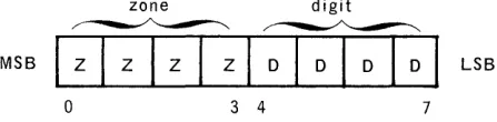
Data can be represented in various forms by the programmer; but certain restrictions are imposed if the data is to be printed or processed arithmetically. The contents of a byte can be considered as a binary number, a decimal number, or two packed decimal numbers, an alphabetic or symbolic character, or logical information. A field used to represent a binary number uses all of the bit positions (except the sign bit) to contain the value. However, each byte in a field representing a decimal number, alphabetic character, or symbol is considered to be divided into zone and digit portions. The zone portion is the most significant four bits; the digit portion is the least significant four bits.
zone digit
~~
MSB
I
z
I
z
I
z
I
z
I DID I DID I
LSBo
3 4 7l.LL 10 Binary Number Representation
Binary numbers in the registers make use of the most significant bit (MSB) as the sign indicator. A 0 in the most significant position indicates a positive number and a 1 indicates a negative number. It should be noted that since the MSB is the sign bit, a binary value of only ±32K may be expressed. Negative numbers are expressed by the two's complement value of the number.
104 c2 0 Hexadecimal Representation
Hexadecimal numbers are those having a radix or base 16. There are 16 digits from
o
through F(15). A hexadecimal digit is used to denote a particular four-bit pattern in the zone or digit portion of a byte representing either a decimal number or an alphabetic or symbolic character. Hexadecimal digits and their decimal equivalents up to 65,535 are given in Table 1-2 along with an example of how to derive the decimal equivalent to a hexadecimal number.HEX DEC HEX
0 0 0
1000 4096 100 2000 8192 200 3000 12288 300 4000 16384 400 5000 20480 500 6000 24576 600 7000 28672 700 8000 32768 800 9000 36864 900
AOOO 40960 AOO BOOO 45056 BOO COOO 49152 COO
0000 53248 000
EOOO 57344 EOO FOOO 61440 FOO
EXAMPLE:
Hexadecimal 39DB to Decimal
DEC HEX
0 256 512 768 1,024 1,280 1,536 1,792 2,048 2,304 2,560 2,816 3,072 3,328 3,584 3,840
3000 = 12,288 900 = 2,304
DO = 208 B = 11
39DB
=
14,811 0 10 20 30 40 50 60 70 80 90 AO BO CO DO EO FO DEC 0 16 32 48 64 80 96 112 128 144 160 176 192 208 224 240Table 1-2. Hexadecimal - Decimal Conversion
HEX DEC
0 0
1 1
2 2
3 3
4 4
5 5
6 6
7 7
8 8
9 9
A 10
B 11
C 12
0 13
E 14
F 15
--U P - 7 5 4 6 L Rev. 1
---,
UNIVAC 9200/9200 11/9300/9300 II
PROCESSOR AND STORAGE
SECTION: 1 P AGE:The expansion of Table 1-2, and tables for the powers of 2 and 16, are given in A ppendix A.
1.4.3. Decimal Number Representation
Decimal numbers are represented either in unpacked form (one digit per byte) or in packed form (two digits per byte). In unpacked form, the byte is divided into zone and digit positions.
zone digit zone digit
~:~:~~~dl
m:
I
:r:1+
I
w:
I
~
I
o
7 8 15The zone portion usually contains a hexadecimal F (1111), which is ignored except in the least significant byte; the zone portion of the least significant byte is inter-preted as the sign of the number. In packed form, digits are contained in both halves of a byte, except the least significant half byte of the field, which is interpreted as the sign of the decimal number.
UNPACKED DECIMAL
The sign of the decimal number is represented by hexadecimal digits A through F. Any other bit configuration is an invalid sign code, which could produce unpredictable res ults.
1.4.3.1. Sign Bits
The binary values of the si gn bits are interpreted as follows:
0000 through 1000 positive number
1001 negative number
1010 positive number - generated by instructions in ASCII mode
1011 negative number - generated by instructions in ASCII mode
1100 positive num ber - generated by instructions in EBCDIC mode
1101 negative number - generated by instructions in EBCDIC mode
1110 positive number
1111 positive number
UP-7546 Rev. 1
UNIVAC 9200/9200 11/9300/9300 II
I
1I
17.~~~_P_R_O_C_E_S_SO~R_A_N_D~S_T_O_R_A_G_E~~~~~~~~~~~~.~_
1.4 .4. Character Representation
An alphabetic symbolic character uses eight bits of a byte and has no sign.
digit digit
~~
~:::::::rtation
I
bib
I
bib
I
bib
I
bib
I
bib
I
bib
I
bib
I
bib
I
o
7 8 151.4.5. Parity Verification
The UNIVAC 9200/9200 11/9300/9300 II Systems processor uses odd parity for error checking. All data read from storage is given a parity check.
1.4.6. OP Codes
1.4.7 ..
The OP code designations are expressed by two hexadecimal digits, in the 8-bit code shown, as follows:
BINARY DECIMAL HEXADECIMAL
0000 0 0
0001 1 1
0010 2 2
0011 3 3
0100 4 4
0101 5 5
0110 6 6
0111 7 7
1000 8 8
1001 9 9
1010 10 A
1011 11 8
1100 12 C
1101 13 0
1110 14 E
1111 15 F
Logical Information
UP·7546 Rev. 1
UNIVAC 9200/9200 11/9300/9300 II
I
')
I
_ _ _ _
P_R_O_C_E_S_S_O_R_A_N_D_S_T_O_R_A_G_E _ _ _ _ _ _ _ _ _ _
~~~
_ _ _
2. PROCESSOR UNIT
2.1. MAIN STORAGE
The maximum number of addressable locations (after installation of the expansion option) is 16,384 for the UNIVAC 9200 System processor, and 32,768 for the UNIVAC 9200 II,
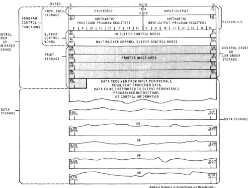
9300, 9300 II System processors. Each addressable location consists of a byte of information containing eight data bits. The first 260 locations are called the privileged or low order storage. Of these, the first 96 byte locations are associated with either the processor program state control or the I/O (executive) program state control and are restricted. The next 32 byte locations are reserved for the buffer control words. The final 132 byte locations of low order storage are reserved for print storage. Main storage byte locations are used to store the following kinds of information: data received from input peripheral units, results of processed data, data to be distributed to output peripherals, programmed instructions, and control information. Figure 2-1 shows the main storage organization, iden tifyin g the byte locations by giving typical addresses in both decimal and (in parentheses) hexadecimal notation.
Each byte contains nine bits, which comprise eight information bits and one parity bit. The bit combination, as interpreted by the various instructions, represents alphabetic, decimal, binary, or logical data.
2.1.1. Privileged and Low Order Storage
The first 260 bytes of storage, called the low order storage, are reserved for specific operation information. Information stored in this area is accessible as needed during the execution of the functions. The first 128 locations, conSisting of 64 locations called privileged storage and 64 locations for buffer control words, are reserved for program control functions. The remaining 132 locations are reserved for print storage, storing the data required for each line of print for the bar printer.
The privileged storage area contains 16 general registers, eight processor program registers, and eight input/ ou tput program registers, each holding two bytes. The processor can reference either of these two sets of eight registers in low order storage. This capability greatly reduces the interrupt handling time because the normal interrupt processing required, when only one set of general registers is provided, is unnecessary. Also the time required for storing the contents of the processor program registers and loading instructions and data into the registers is greatly red uced by the use of two sets of registers.
UP-7546
Rev. 1
L
UNIVAC 9200/9200 11/9300/9300 "
PROCESSOR AND STORAGE
SECTION: 2 PAG E:CONTROL OF:DER
OR LOW ORDEI~
STORAGE
DATA STORAGE
PROGRAM CONTROL
BYTES PRIVILEGED STORAGE
BUFFER CONTROL WORDS
PRINT STORAGE
PROCESSOR ARITHMETIC PROCESSOR PROGRAM REGISTERS
9 10 12
15 16
15 16
(F) (10) INPUT/OUTPUT
ARITHMETIC
INPUT/OUTPUT PROGRAM REGISTERS
8 9
DATA RECEIVED FROM INPUT PERIPHERALS, RESUL TS OF PROCESSED DATA,
DATA TO BE DISTRIBUTED TO OUTPUT PERIPHERALS, PROGRAMMED INSTRUCTIONS,
oR CONTROL INFORMATION
ff,160
---~---~
8 191I:r
~
~
(2FEO)~ ____ OR ____________ ~~---12,2
1
87 (2FFF)I
OR _---~----~~
~-
~---
(3FFF) 16,3831~ I
OR
FE
(SF EO) ---~:?P1
(5FFF)===== _____
~---r
i;,;'IJ
_ _ _ _ _ _ _ _ _ _ _ ... ~_F.L.EO_) _ _ _ _ _ _ _ _ _ _ _ _ _ _ _ _ _ _ _ _ _ _ _ _ _ _ _ _ _ _ _ ....I__"J,
(Address Numbers in Parentheses are Hexadecimal)
Figure 2-1. Main Storage Organization
2.1.2. Storage Boundaries
RESTRICTED
CONTROL ORDER OR LOW ORDER STORAGE
DATA STORAGE
Bytes may be addressed separately or in groups. Two consecutive bytes constitute a halfword when the more significant byte is found at an even number address. Instructions occupy 4 or 6 bytes and are restricted to halfword boundaries. For instructions which imply a fixed length field of more than one byte, the operands are again restricted to halfword boundaries. If the field lengths are variable, there are no boundary restrictions. A 11 fixed and variable length storage operands (operands being the addres s portion of an instruction) are addressed at the most significant byte position, regardless of whether the instruction is processed from left to right or from right to left. For variable size operands, the length is specified as a binary number which is one less than the actual count, thus a length count of one is expressed by all zeros in the length field.
UP-7546 Rev. 1
UNIVAC 9200/9200 11/9300/9300 "
I
2I
3,~~~_P_R_O_C_E_S_SO~R_A_N_D~S_T_O_R_A_G_E~~~~~~~~~~~~~.~_
Bytes in any storage are consecutively numbered starting at 0, up to a number which is less by one than the storage size, according to the following:
Maximum Address A vailable in Number
9200 9200 II 9300 9300 II
8,191 X X X
12,287 X X X
16,383 X X X X
24,575 X X X
32,767 X X X
2.1.3. Parity Checking
Each byte of storage has, in addition to the eight information bits, a ninth, or parity bit. The parity bit is set to 0 or 1 as may be necessary to make an odd number of 1 bits in the byte. This parity check bit is checked as data are read out of storage and is regenerated when data are altered as a result of processing. Parity is also generated when data are introd uced into the processor from peripherals or other sources that do not already have a parity bit included in their data format. In other parts of this description of the processor's operation, the parity bit will not be mentioned except as it may be related to a possible error condition. If a processor parity error occurs, the processor will stop, and all input/output: devices in use will continue to normal termination. A parity error that is detected during the transfer of data to and from the attached peripherals is considered a peripheral parity error and is discussed in 2.3.8.
2.1.4. Interrupts
An interrupt is the stopping of a process (in the processor) in such a way that it can be resumed; the reason for an interrupt is to afford opportunity for the required execution .of another process external to the interrupted process but related to it. Interrupts are
inhibited if processing is in the input/output state or if an inhibit interrupt is specified by programmed instruction. An interrupt can occur as a result of any of the following conditions:
• normal completion of an input or output function
• input or output function ended due to abnormal condition
• processing of a.supervisor request call (SRC) instruction
• interval time (normally one second) exceeded.
An interrupt from a peripheral device can occur only if priority is granted to the device requesting the interrupt. When the request is granted, the following steps occur:
(1) The interrupt request is stored in appropriate indicators.
(2) The status code for the device is loaded into location 66 (42) and the device number is loaded into location 67 (43).
UP··7546
I
Rev. 1 ~
UNIVAC 9200/9200 11/9300/9300 II
PROCESSOR AND STORAGE
2.2. PROCESSOR CONTROL
2
SECTION: PA G E:
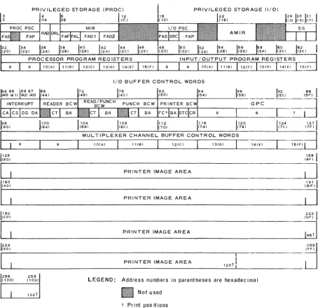
The low-order storage area, locations 0 through 259 (103), is used for temporary storage of data required for processing an instruction and for the instruction and for the instruc-tion itself. This storage is divided into two major parts (processor, and input/output) and several minor parts, as illustrated in Figure 2-2. The processor and the input/ output portions of privileged storage are used separately; at any given time the one used depends on the Program State Control. The fields within the low-order storage and the adjacent buffer control word areas are as follows:
PROC PSC
FAS
FAP
RAD
ORL
MIR
FAF
FAL
FAD1
FAD2
I/O
PSCFAS
SRC
FAP
AMIR
SS
INTERRUPT
CA
CS
DS
DA
BCW
CT
BA
Processor Program State Control
Fixed Address Status (Condition Code)
Fixed Address Pointer (address of first byte of next instruction)
Res tricted A Her/D isplay
Operator Request Location
Machine Instruction Register
Fixed Address Function (Operation Code)
Operand Length/Register Address/Immediate Data
Address of Operand 1
Address of Operand 2
Input/Output Program State Control
Fixed Address Status
Supervisor Request Call
Fixed Address Pointer
Restart Instruction Register
Special Status Storage for General Purpose Channel
Interrupt Entry for General Purpose Channel
Device Address (Selector Channel Only)
Channel Status (Selector Channel Only)
Device Status
Device Address
Buffer Control Word (Reader, Read/Punch, Punch)
Count (number of columns to be read or punched)
Base Address (address of least significant byte of input or output data)
UP-7546 Rev. 1
UNIVAC 9200/9200 11/9300/9300 II
I
')
I
,~~~_P_R_O_C_E_S_S_O_R_A_N_D~ST_O~R_A_G_E~~~~~~~~~~~E:
5
PRINTER BCW
FC
BA
STC
CR
GPC
Forms Control
Base Address
Starting Code
Code Register
General Purpose Channel (reserved for multiplexer channel buffer control' words in UNIVAC 9300/9300 II Systems processor.)
PRIVILEGED STORAGE (PROC) PRIVILEGED STORAGE (I/O)
Ig6
AMIR
(20) (22) (24) (26) 150 154 1
56 158
160 162 (32) (34) (36) (38) (3A) (3e) _ _ (3_E:)
5=
2 134 36 138PROCESSOR PROGRAM REGISTERS INPUT/OUTPUT PROGFIAM REGISTERS ~
8
J=
9 10(A) 11(6) 9 10(A) 11(6) 12(CiG(0) 114(1~5~I/O BUFFER CONTROL WORDS
1
64 65 ~615 67 68 (40) (4 1 )J~2) (43) (44)
~
NTERRUPT READERr ... .
CAe Sll :JL.: D S D A :::::::~::::: C T
:.:~::.:::::
192 95 I
~-~--a(5F)
6
I
7-
._---1 88 (58)
1
96
(60) (64) (68) (6e) (70) (74) (78) (7e) (7F)
tia
1100
1
104 1108 1112 1116 1120 1124 127/
----~---M--U-L-T--IP-L--E-X~E--R--C-H-A--N-N-E-L~B--U-F-F-E-R--C-O~N-T-R--O-L--W-O-R--D~S---~-~
1(80) 128
c=
1 160 (AO)
c=
1 192
(CO)
9 10(A) 11(6) 12(e) 13(0) 14(E) ~D
PRINTER IMAGE AREA
PRINTER IMAGE AREA
159
I
(9F)-~
191 1
(SF)
~
223 1 (OF)
~
PRINTER IMAGE AREA- I
---~
1 224
(EO) (FF) 2551
~
______________________ P_R_I N_T_E_R __ I_M_A __ G_E_A_R_E_A _________ 12_0_t-'!!...-__ . _ _ _ _ _ _ -_._--J
1256 (100) (103) 259 1
C=~~d
LEGEND: Address numbers in parentheses are hexadec ima I
l~l~l~l~l~l~l~l~1
Not use d t Print pos itions *FC=Bits 45670001 space one line 0010 space two lines 1xxx paper loop control
UNIVAC 9200/9200 11/9300/9300 II
PROCESSOR AND STORAGE
I
PAGE' 6UP~7546L
Rev. 1
- - - -
----2.2.1. Program State Control
Program state control is a means of changing from one program state (processor or input/output) to the other. The state control determines which portion of privileged storage (processor or input/output) is used for processing instructions. The addressing of privileged storage under processor state control results in an error stop. Privileged storage may, however, be addressed under input/output state control without an error stop. Input/output devices may read out data from privileged storage without an error stop, but only during initial load mayan input/output device write into privileged storage.
The processor and input/output states differ significantly in the following respects:
Processor State
Processor portion of privileged storage used for processing instruction.
Input/Output State
Input/output portion of privileged storage used for processing ins tructions.
Selected only by special instruction.
Selected by conditions such as an interrupt from a peripheral unit or general clear"
Interrupt inhibited only by program ins tru ction.
Interrupt always inhibited.
Accessing privileged storage by an instruction generates processor abnormal (address error) condition.
Privileged storage can be accessed by an instruction with no (privileged storage) address error. '
2.2.1.1. Processor Program State Control Word (Bytes 0-3)
The processor program state control (PPSC) word has the following organization:
0 1 2 3
(0) (01) (02) (03)
E
cc
AOOOOOOOOOO:O~O
_----:---r-'---7 8 15 16
---~---
J24
3
:J
P
I-
FAS-I
t--I-- - - -FAP-I
P ROC PSC - - - -....
-,
where: CC
=
condition code A = ASCII control bit1 for ASCII
o
for EBCDICo
= unspecifiedP
=
address of first byte of next instructionThe user's program is normally executed in the processor program state. In this state, an interrupt is never inhibited except by program instruction.
LOCATION
BYTES
UP-7546 Rev. 1
UNIVAC 9200/9200 11/9300/9300 II
PROCESSOR AND STORAGE
2.2.1.2. Input/Output Program State Control Word (Bytes 16-19)
2 SECTION:
The input/output program state control (I/O PSC) word has the following organization:
16 17 18
(10) (11) (12)
E
0J
15116
2
CC A 00000 SRC P
r---
FAS"1
4 SRC
·1-I -
I/O PSCwhere: CC = condition
A = ASCII control bit 1 for ASCII
o
for EBCDICo
=
unspecifiedSRC = supervisor request call byte
p = address of first byte of next instruction
19 (13 )
2J4
FAP
2.2.2. Restricted Alter/Display and Operator Request (Bytes 4, 5)
3
.. :J
P--1
-1
The restricted alter/display (RAD) location and the operator request location (ORL)
LOCATION
BYTES
BITS
are storage areas in low order storage used for entering information through the console of the computer. This function is performed in connection with certain software routines.
2.2.3., Machine Instruction Register (Bytes 6-11)
The machine instruction register (MIR) is loaded with the first instruction to be executed when a program is loaded; thereafter, the register will contain the current instruction in the pro gram.
I - - - - F A F I
I.
FAL.1.
FAD1 ..I6 7 8 9
E
0 (07) (08) (09)J
116
2
I
3 · ·-J
-X Xl P1
15 31
E
4 5P2
47
10 11
(OA) (OB)
II
I-
FAD2LOCATION BYTES
Rev. 1
UNIVAC 9200/9200 1119300/9300 II
PROCESSOR AND STORAGE
SECTION: 28 PA G E: U P " 7 5 4 6 L
,---~---~~---~---where: X
=
operation codeXl operation length/register address/immediate data
Pl address of Operand 1 P 2
=
address of Operand 22.2.4. Restart Instruction Register (Bytes 22-25)
22
The restart instruction register (AMIR) is used to store a branch instruction. It is the first instruction executed when a restart procedure is initiated by the operation of the first the CLEAR switch and then the START switch at the control console.
24 25
(16)
23
(17) (18) (19) LOCATION
E
JP 1
o
____~1~5~ll~6~
_______ p_23 ______~2=3~12~4~
______ :_4 ___~ :~T~ES
where: PI = present program address
P 2 = register of next instruction in logical sequence
P3} __ address to which instruction branches
P4
2.2.5. Special Status (Bytes 29-31)
This area of storage is reserved for use by the Univac customer engineer. See 2.3.8.
2.2.6. Processor Program Register (Bytes 32-47) and Input/Output Program Registers (Bytes 48-63)
A separate group of eight registers is reserved in storage for each program state. The registers for any particular program state can be accessed only when the system is in the corresponding program state. The addresses of the registers are 10002 through 11112, Each register is two bytes long.
2.2.7. Device Status (Byte 66) and Device Address (Byte 67)
64
The device status (DS) and device address (DA) locations are storage areas in lower memory to receive device status (condition) and address fields during input/output operations from the peripheral devices.
65 66 6'7
(40) (41 ) (42) (43) LOCATION
E:o
1
oo~o:r
2J24
3
J
BYTESP PI
15 16 BITS
14 CA
, I
J CS'I'
os
, I
J OAUP-7546 Rev. 1
UNIVAC 9200/9200 11/9300/9300 II
I
2I
9, _ _ _ _ P_R_O_C_E_S_S_O_R_A_N_D_S_T_O_R_A_G_E _ _ _ _ _ ... _ _ _ _
~~~,_,
__where: 0
=
for selector channel use only, otherwise unspecified P device sta tusPI device address
Location 64 (40) and 65 (41) are used to store the device address and channel status respectively when interrupt occurs for devices operating exclusively by