[54] CIRCUIT ARRANGEMENT FOR THE
RECOGNITION OF IMPERMISSABLE PHASE ERRORS IN A PHASE LOCKED LOOP
[75] Inventor: Erik Solhjell, Oslo, Norway
[73] Assignee: Tandberg Data A/S, Oslo, Norway
[21] Appl. No.: 70,191
[22] Filed: Jul. 6, 1987
[30]
Foreign Application Priority Data
Dec. 22, 1986 [DE] Fed. Rep. of Germany ... .. 3643966
[51] Int. Cl.4 ... .. H04L 7/02 [52] US. Cl. ... .. 375/120; 331/14
[58] Field of Search ... .. 375/81, 120; 329/50, 329/122; 331/1 A, 14, 17, 25; 328/155; 360/51
[56] References Cited '
U.S. PATENT DOCUMENTS
4,517,531 5/1985 Tan et a1. ... .. 331/14 4,563,657 l/1986 Qureshi et a1. 331/14 4,596,963 6/1986 Lawton et a1. 331/14 4,607,296 8/1986 Smidth ... .. 360/51 4,644,567 2/1987 Artun et al. ... .. 375/120
FOREIGN PATENT DOCUMENTS
0141946 8/1984 European Pat. Off. . 0153107 8/1985 European Pat. Off. . 3115057Al 10/1982 Fed. Rep. of Germany .
OTHER PUBLICATIONS
IBM Technical Disclosure Bulletin, vol. 8, No. 12,
May, 1966, “Error Feedback Clocking” by W. T. Har
nett, pp. 1742-1744.
1298 Telecom. & Radio Engineering, vol. 31/32, No. 8
(1977.08) “A Synchronization System with Digital
Control in High-Speed Data Transmission”, by A. S. Georgiyev, pp. 22-24.
IBM Technical Disclosure Bulletin, vol. 28, No. 5, Oct. 1985, “Voter Frequency Control Loop for Global Common Clock”, pp. 1986 and 1987.
Primary Examiner—Benedict V. Safourek
Attorney, Agent, or Firm—1-Iill, Van Santen, Steadman &
Simpson
[57] ABSTRACT
In a retrieval of data stored on a magnetic medium, a
phase locked loop is employed for clocking data signals
allocated to the data. This phase locked loop generates clock signals synchronized with the data signals. The data signals are subject to various distortions and are
subject to a shift of individual data signals dependent on
the recorded data. To prevent the phase locked loop
from processing these shifts as phase or frequency er rors, a switch stage is provided which inhibits the con trol in the phase locked loop give the occurrence of such shifts. -The switch stage contains a time-delay stage
and a comparator. The control is inhibited when succes sive phase differences between the data signals and the clock signals appear in opposite directions.
7 Claims, 3 Drawing Sheets
/FU\P\-FLOP
G1
P11
P2 8
F11 —=3,F21-=
EH1
I ‘ .__
.B.
/' (P11 We} 68%
T- " COMPARATOR
1. 1C2}, F12
E “T
F22 L a
26 [E52
(PHASE
&—| '
B7
US. Patent
Feb. 7, 1989
Sheet 1 of3
4,803,704
E+
_
nU\\
.
L
E
L.
V
P _
D?+
Du
. E E .
.I
L _ n
F
El .
W. L
ml
W4
r“
_
D E .
H
r E W .
A
m
m _ .
H .
_|.
W
Pi.-.
.L
D
“nun
PhD/-
EM
G
I
“R
A
TAM
D
HM
5
PM
D
6mm; c
‘M
AE
FW-
8
WW
W
D\LnU
D
S
VOLTAGE CONTROLLED USEILLATUR
FIG 2
l
R
DUEL-Ll
GATE
EH1
EU
AMPLIFIER
CS
COMPARATOR
FLIP - FLUP
FIG 3
EHASE EUMPARAT
C ->
FIG 5
FLIP-FLOP
/
US. Patent
Feb. 7, 1989
Sheet 3 01's‘
4,803,704
FIG 7
R.
m
M
AH .
TB
.|.|._ Om.
Arr.
Us LB
4 G C
_.
om
\1.
I11
R DH L . 1L
WW. .] CL , __
W
N
S
L01
0 C . O0
2
5
.1. all.
_
*3R|_
6 Cu
80
nlvvl 0G
2
M
wllm
‘I:
rim
m
. /
P
W
2
O
P
[I
a
l.
F
\
_\
H
W
,l
H
.L/
3+
.
/a|
mum
3
“Chm
F>
(
_ A
DH
‘I.
Em
M
SM
3
S. u
AAI.PL U I.
HP
P
E
PM
W
U
T
Plv
‘IE
RECOGNITION OF IMPERMISSABLE PHASE
ERRORS IN A PHASE LOCKED LOOP
BACKGROUND OF THE INVENTION
1. Field of the Invention
The invention is directed to a circuit arrangement for the recognition of impermissable phase errors in a phase
locked loop wherein means are provided for generating
phase signals by a phase comparison of binary data signals and clock signals and wherein a repetition rate of clock signals generated in an oscillator is modi?ed de pendent on the phase signals.
2. Description of the Prior Art
In a playback of data recorded on a recording me
dium, for example on a magnetic tape or on a magnetic disk, the data signals output by a transducer, for exam ple, a magnetic head, can be distorted in various ways. The distortions can occur as a result of ?uctuations in the relative speed between the recording medium and the transducer. This can occur due to noise, dust parti
cles, inadequacies in the surface of the recording me dium, or, in the case of a magnetic recording medium,
due to the particular properties of the magnetic parti
cles. In order to assure the best possible playback of the
data stored by the data signals, a phase locked loop, also referred to as a PLL, is employed in order to generate lock signals which are synchronized with the played back data signals. The phase locked loop can be de
signed both as an analog as well as a digital circuit.
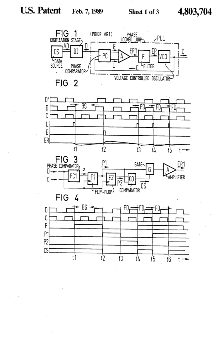
Such a phase locked loop designed as an analog cir cuit is shown in FIG. 1. The analog data signals AD
proceed from a data source DS, for example, a magnetic
head of a magnetic tape recorder means or of a mag
netic disk storage, to a digitization stage DI which gen
erates binary data signals D from the analog data sig
nals. These data signals D are supplied to the phase locked loop PLL which generates clock signals C serv ing as reference clock signals. The clock signals C are
generated in a voltage-controlled oscillation VCO and, just like the data signals D, are supplied to a phase
comparator PC. Dependent upon whether the data signals D lead or trail the clock signals C, this generates phase signals E or L whose duration corresponds to the amount of lead or trail. An ampli?er A generates an
error signal ERl from these phase signals EL and con
ducts it to a ?lter F, usually a low-pass ?lter, which
generates a control signal ER and emits this to the volt
age-controlled oscillator VCO. This modi?es the fre quency of the clock signals C dependent on the momen
tary value of the control signal ER such that a phase difference between the data signals D and the clock signals C is opposed.
In the illustration of FIG. 2, the data signals D’ are
ideal data signals wherein the spacings of the leading edges differ by wholemumbered factors dependent on
the data to be recorded. .
It can occur in a recording onto a recording medium that successive data signals D are shifted in opposite
directions. This particularly occurs when the spacings of the data signals change and the data signals D are then respectively shifted toward the gap which thus arises. This event is also referred to as “bit shift” and is identi?ed as BS in FIG. 2. However, it can also occur
that, due for example to a ?uctuation in the relative
speed between the recording medium and the trans
ducer, the data signals D are shifted in one direction, 10 15 35 45 55 60 65
In both cases, the phase locked loop PLL has the job
of eliminating the in?uences of these effects. Given a frequency deviation FD, there is no dif?culty in modi
fying the frequency of the clock signals C in one direc tion. However, there is a risk that in the ?rst, data dependent shift as shown, for example, at point in time
T1, the oscillator VCO is adjusted in the same way as it
is adjusted given a frequency deviation FD correspond ing to a trailing of the data signals D. In the following data signal D as shown, for example at point in time T2, the data signal D is leading in comparison to the clock
signal C. It can thus occur that the synchronization between the data signals D and the clock signals C is lost, and thus the recorded data cannot be unambigu
ously re-acquired.
Given a trailing of the data signals D in comparison to the clock signals C, phase signals L are generated at points in time T1 and T3 through T5, whereas a phase signal E is generated at point in time T2 given leading
data signals. The ampli?er A and the ?lter F generate
the control signal ER from the phase signals E and L, this control signal ER being supplied to the oscillator VCO in order to modify the frequency of the clock signal C to assure the best possible synchronization
between the clock signals C and the data signals D. The filter F is normally in position to compensate the
data dependent bit shifts BS. However, given storages of which especially high demands are made, it can occur that the elimination of the information-dependent bit shifts is extremely difficult without disturbing the high-frequency behavior of the phase locked loop PLL.
SUMMARY OF THE INVENTION
It is therefore an object of the invention to specify a circuit arrangement which eliminates the influences of
impermissable phase errors as a consequence of data dependent shifts without disturbing the high-frequency behavior of the phase locked loop.
According to the invention, a switching means is provided for identifying a phase difference between
two successive data signals and corresponding clock signals, for recognizing an impermissable phase error when two successive phase differences exhibit direc tions opposite one another, and for inhibiting said means for modifying the repetition rate of the clock signals given presence of such an impermissable phase error.
The present invention is based on the fact that the
data-dependent shifts as de?ned here are always caused
by two successive data signals being shifted in mutually opposite directions. These shifts are recognized with
the assistance of a switching stage, and the control by
the phase locked loop is inhibited.
BRIEF DESCRIPTION OF THE DRAWINGS
FIG. 1 is a block circuit diagram of a known phase
locked loop;
FIG. 2 is a signal pattern of signals at various points
of the phase locked loop illustrated in FIG. 1; FIG. 3 is a block circuit diagram of a circuit arrange
ment of the invention;
FIG. 4 is a time diagram of signals at various points of the circuit arrangement shown in FIG. 3;
4,803,704
3
FIG. 6 shows time diagrams of signals at various points of the circuit arrangement of FIG. 5; and
FIG. 7 is an exemplary embodiment of a circuit ar rangement provided in a digital phase locked loop in
accordance with the invention.
DESCRIPTION OF THE PREFERRED
EMBODIMENTS
In the block circuit diagram shown in FIG. 3, the phase comparator PCI corresponds to the phase com parator shown in FIG. 1 and essentially differs there from only in that, instead of the phase signals E and L, it only respectively outputs one phase signal P whose binary value indicates whether a data signal D is leading
or trailing a clock signal C. The phase signals P are supplied to a time delay element formed of two ?ip
?ops F1 and F2 which respectively delay the phase signals P in accordance with the spacing of the data signals D, and outputs the delayed phase signals P1 and P2. The delayed phase signals P1 and P2 are supplied to a comparator CO which outputs the control signals CS
with which the phase signals P1 are inhibited when two
successive, data-dependent bit shifts BS occur in oppo
site directions. The inhibiting occurs by means of a gate
G which is connected preceding an ampli?er A and
which emits a control signal ER1 only when a control
signal CS simultaneously occurs with the phase signal P1.
In the illustration in FIG. 4, the phase detector PC1 determines at point in times T1 that the data signal D is trailing the clock signal C and the phase signal P as sumes the binary value 1. At point in time t2, the phase detector PCl determines that the data signal D is lead
ing the clock signal C and the phase signal P again
assumes the binary value 0. Since the data signal D issupplied to the clock input of the ?ip-?op F1 at whose data input the phase signal P is present, the flip-flop F1 is set at point in time t2. With the trailing edge of the next data signal D, the flip-?op F1 is again reset at point
in time 33 and the ?ip-?op F2 is set. It is assumed at
point in time t4, t5, and t6 that the data signals D are
trailing the clock signals C as a consequence of a fre
quency deviation FD. The phase signal P thus respec tively assumes the binary value 1 at these points in time
or retains this binary value 1. In a corresponding way,
the phase signals P1 and P2 assume the binary value 1 with the respectively following data signals D.
Between points in time t2 and t4, the comparator CO
inhibits the phase signals P1 since these are allocated to
mutually opposite phase shifts. Up to point in time t2, between points in time t4 and t5, and following point in time t6, the phase signals P1, however, are connected
through as control signals ER1 in order to maintain the
synchronization between the data signals D and the clock signals C. A control signal CS for inhibiting the gate G is always output when the phase signals P1 and
P2 exhibit the same binary value. For this purpose, for example, the comparator CO can be designed as an
equivalence gate. The gate G, for example, can be de
signed as a tristate gate wherein the output is switched
to high-resistance by the control signal CS and is always enabled by the control signal CS only when no data dependent shift of the data signals D occur.
The circuit diagram shown in FIG. 5 shows a more detailed illustration of the circuit arrangement of FIG.
3. In this circuit diagram, the phase comparator PC2 has
two outputs in accordance with the block circuit dia gram in FIG. 1 at which the phase signals E and L are
5 20 25 30 35 45 50 55 60 65
4
output. Each of the phase signals E or L is delayed by
two period durations of the data signals D in a two stage
time-delay element formed of flip-?ops F11, F12, F21, and F22. For this purpose, the clock inputs of the ?ip
fiops are supplied with the data signals D inverted by an
inverter I. A phase signal L is output when a data signal
D trails a clock signal C and a phase signal E is output when a data signal D leads a clock signal C. Gates G1
through G3 check whether the delayed phase signals P11 and P21 or P12 and P22 are identical. Further gates G4, G5, and G6 check whether impermissable condi tions of the ?ip-?ops F11 through F22 occur when the phase signals L and E appear simultaneously. In this case, a gate G7 prevents the phase signal P22 from being connected through to the ampli?er A2 via the
gate GB, and from being output at the ampli?er A2 as a control signal ER1. In case no impermissable conditions occur, a control signal CS1 output at the gate G3 is
supplied to the gate G8 as control signal CS2 via the gate G7. This control signal CS2 always inhibits the gate G8_ when successive phase shifts appear in opposite directions, and thus data-dependent shifts of the data
signals D are indicated. The control signal CS2 can also be synchronized by a further ?ip-?op in order to avoid
noise peaks on the signal supplied to the ampli?er A2.
The time diagram shown in FIG. 6 differs from the
time diagram shown in FIG. 4 since ?rst, the two phase
signals L and E are generated instead of one phase
signal P. It is assumed that the data signal D is leading the clock signal C at point in time t1, is trailing it at points in time t4 and t5, and is in-phase at points in time
t6 and t7. The data—dependent bit shift BS of the data signals D occurs at points in time t2 and t3. In a way
corresponding to that in FIG. 4, the phase signals L and E are each delayed by two period durations of the data signals D. Since the phase shifts between the data sig
nals and the clock signals C occur in the same direction
only at points in time t4 and t5, a corresponding control signal ER1 is output only between the points in time t6 and t7. Given successive, mutually oppositely directed phase shifts BS between the data signals D and the clock signal C, the circuit arrangement shown in FIG. 5 inhibits the control by the phase locked- loop PLL.
Given the circuit diagram shown in FIG. 5, the phase comparator PC2 is designed such that it stores the phase signals L and E up to the respective appearance of the next data signal D. It is also possible to employ a phase comparator PC2 wherein, as shown in FIG. 2, the phase
signals L and E each comprise a duration which corre sponds to the phase error. These pulses are converted
into a corresponding voltage which is sensed and stored until they are switched through by the gate G8 while the control signal CS2 is active.
The circuit arrangement of the invention can also be
employed in a completely digitalized phase locked loop. Various solutions are possible therefor. A relatively simple solution is shown in FIG. 7. The data signals D
and the clock signals C are again supplied to a phase
comparator PC3 which generates a phase signal P be—
tween a respective data signal D and a clock signal C.
The phase signals P are each delayed by a period dura tion of the data signals D by two ?ip-?ops F31 and F32
and are checked by an equivalence gate serving as com parator C02 to see whether the data signals P31 and
P32 exhibit an unequal binary value, and thus indicate phase shifts BS in mutually opposite directions.
Instead of the voltage-controlled oscillator VCO, an
by an inverter II. The parallel outputs of the shift regis ter SR are each connected to an input of AND gates
G11 through G14 whose outputs are each supplied to an OR gate G15. The clock signals C are output at the
output of the OR gate G15. '
The shift register SR serves as a frequency divider wherein a respective output signal at one output is slightly delayed in comparison to an output signal at a
preceding output. A data selector SEL selects one of - the gates G11 through G14 in order to supply the corre
sponding output signal of the shift register SR to the
phase comparator PC3 as clock signal C via the OR gate G15. The data selector SEL is driven by a counter CNTR at whose clock input the data signals D are
present, at whose increment/deincrement control input the phase signal P31 is present, and at whose enable input the output signal of the comparator C02 is pres
ent. Dependent on the binary value of the phase signal P31, the counter is incremented or deincremented with
every data signal D depending upon ‘whether a leading or a trailing of a data signal D in comparison to a clock signal C is to be opposed. The incrementing/deincre menting of the counter CNTR, however, occurs only when the comparator CO2 emits an enable signal, i.e.
when the phase differences between two successive
data signals D and the corresponding clock signals C exhibit the correct direction. In case the phase differ
ences of the successive data signals D exhibit different
directions, the counter CNTR is inhibited in order to guarantee a faultless synchronization between the data
signals D and the clock signals C.
Although various minor changes and modi?cations might be proposed by those skilled in the art, it will be
20
25
35
understood that I with to include within the claims of 40
the patent warranted hereon all such changes and modi ?cations as reasonably come within my contribution to
the art.
I claim as my invention:
1. A phase-locked loop circuit arrangement for rec )ognition of impermissable phase errors in binary data
signals fed to the phaseglocked loop, comprising:
an oscillator means for generating clock signals;
means for generating phase signals indicating phase differences between said binary data signals and said clock signals by a phase comparison;
45
50
55
65
signals dependent on said phase signals; and a switching means connected to receive said binary
data signals and said phase signals for recognizing
impermissable phase errors when two successive
phase differences between said binary data signals and said clock signals have directions opposite one another, and for inhibiting said means for modify ing the repetition rate of said clock signals given presence of said impermissable phase errors.
2. A circuit arrangement according to claim 1 wherein the switching means has a time-delay means for
delaying the phase signals by a respective cycle time of
the binary data signals and for outputting second and
third phase signals delayed by a cycle time with respect
to one another, and a comparator means connected to
the time delay means for comparing the second and
third phase signals.
3. A circuit arrangement according to claim 2
wherein the time delay means is formed of two clock controlled ?ip-?ops.
4. A circuit arrangement according to claim 3
wherein the comparator means is formed of an equiva
lence gate having an output connected to said means for
modifying.
5. A circuit arrangement according to claim 2 wherein a filter is arranged between said means for
generating phase signals and said oscillator means, and
said switching means inhibiting control of the phase
locked loop by inhibiting a transmission of said second
phase signals to said ?lter.
6. A circuit arrangement according to claim 1 wherein said switching means inhibits said means for
modifying the repetition rate of the clock signals by inhibiting an analog control signal generated by said switching means and supplied to the oscillator means.
7. A method for recognition of impermissable phase differences in binary data signals fed to a phase locked
loop, comprising steps of:
generating clock signals;
generating phase signals by a phase comparison of
said binary data signals and said clock signals; modifying a repetition rate of said clock signals de
pendent on said phase signals; and
recognizing impermissable phase errors when two successive phase differences between said binary data signals and said clock signals exhibit directions opposite one another, and inhibiting the modi?ca tion of the repetition rate of the clock signals given presence of such impermissable phase errors.