Scalable IC Platform for Smart Cameras
Richard P. Kleihorst
Philips Research Laboratories, Professor Holstlaan 4, 5656 AA Eindhoven, The Netherlands Email:[email protected]
Anteneh A. Abbo
Philips Research Laboratories, Professor Holstlaan 4, 5656 AA Eindhoven, The Netherlands Email:[email protected]
Vishal Choudhary
Philips Research Laboratories, Professor Holstlaan 4, 5656 AA Eindhoven, The Netherlands Email:[email protected]
Harry Broers
Philips Industrial Vision, P.O.Box 218, 5600 MD Eindhoven, The Netherlands Email:[email protected]
Received 19 December 2003; Revised 24 January 2005
Smart cameras are among the emerging new fields of electronics. The points of interest are in the application areas, software and IC development. In order to reduce cost, it is worthwhile to invest in a single architecture that can be scaled for the various application areas in performance (and resulting power consumption). In this paper, we show that the combination of an SIMD (single-instruction multiple-data) processor and a general-purpose DSP is very advantageous for the image processing tasks encountered in smart cameras. While the SIMD processor gives the very high performance necessary by exploiting the inherent data parallelism found in the pixel crunching part of the algorithms, the DSP offers a friendly approach to the more complex tasks. The paper continues to motivate that SIMD processors have very convenient scaling properties in silicon, making the complete, SIMD-DSP architecture suitable for different application areas without changing the software suite. Analysis of the changes in power consumption due to scaling shows that for typical image processing tasks, it is beneficial to scale the SIMD processor to use the maximum level of parallelism available in the algorithm if the IC supply voltage can be lowered. If silicon cost is of importance, the parallelism of the processor should be scaled to just reach the desired performance given the speed of the silicon.
Keywords and phrases:smart cameras, IC architectures, image processing, SIMD, parallel processing, architecture scaling.
1. INTRODUCTION
Real-time video processing on (low-cost and low-power) programmable platforms is now becoming possible thanks to advances in integration techniques [1,2,3,4]. This is relevant to a number of applications such as mobile com-munications, home robotics, and even industrial image pro-cessing [5,6]. It is important that these platforms are pro-grammable since new applications for smart cameras emerge every month. The complexity (and possible error-proneness) of the algorithms and the fickleness of real-life scenes are also strongly motivating complete programmability. Repeatedly building application-specific ICs or weakly programmable ICs is simply too costly and by far not sufficient for this changing market.
It seems like a daunting task to create programmable hardware that is able to process multimillion pixels per
second for complex decision tasks. However, we will show in this paper that this is possible by exploiting the inherent parallelism present in the various levels of image processing. A desirable “silicon” property of the resulting parallel ar-chitectures is that they are easily scaled up or down in perfor-mance and/or power consumption whenever the application changes. This not only lowers the need to develop new ar-chitectures from scratch for new vision application areas, but it also allows the design team to use the same software suite with only some settings changed in include files. This signifi-cantly reduces the overall cost of vision solutions as they can be reused among the portfolio of the producer.
Low level
Intermediate level
High level
(Early) pixel processing Image improvement Edge enhancement Convolution kernels Object processing Shape analysis/coding Segmentation
Decision-making Real-time OS Networking
Figure1: Algorithm classification with respect to the type of oper-ations.
been written about general purpose DSPs, so we will mainly focus in this paper on the merits of SIMD processors for the computationally demanding image processing tasks. Af-ter reading the paper, it will be clear that they have unique and very clear merits from a silicon and algorithmic point of view for realistic IC implementations of programmable smart cameras.
This paper deals with hardware processor architectures and their properties for scalable platforms. However, de-signing an easy-to-use software environment for these scal-able platforms with multiple processor cores is of course an immense task. Even though all processors might be pro-grammable in a similar language, still (automatic) decisions have to be made to decide on which processor to run which task, when, and how to communicate data. A recent result of the smart camera project is a programming method where algorithmic kernels in the shape of skeletons are used to de-scribe the applications. Based on the available processor cores and memory in the final (scaled) architecture, different skele-tons are chosen, linked, and scheduled. The virtue of this de-sign suite is that several skeletons are available for a certain task, optimized for different processor cores. An implemen-tation of a complete application can now survive scaling of the hardware. For more information on this software envi-ronment, the interested reader is kindly referred to [8].
The remainder of the paper is organized as follows. In Section 2, we show how well-known processor architectures map to the image processing algorithms.Section 3deals with some application areas and their performance demands. This is followed by the proposed SIMD-VLIW-based vision plat-form for smart cameras inSection 4. The scaling properties of SIMD regarding silicon are discussed inSection 5. Finally, conclusions are drawn inSection 6.
2. ALGORITHM CLASSIFICATION
Applications on smart cameras have typically as input im-ages or life video from the observed scene and produce low-rate data output in the form of decisions or identification re-sults. Among the examples that are worked on now are per-son and object identification, gesture control, event recogni-tion, and data measurement. More challenging applications are expected to come in the near future.
Low level
Intermediate level
High level
Lots of pixels: 1, . . . ,1000 Mbps Similar processing per pixel
Lots of objects: 1, . . . ,300 k objects/second
Similar processing per objects/group
Some decision tasks Complex processing
Figure2: Data entities with processing characteristics and possible ways to increase performance by exploiting parallelism.
The algorithms in the application areas of smart cameras can be grouped into three levels:low-level,intermediate-level, andhigh-leveltasks. Figures1and2show the task classifica-tion and the corresponding data entities, respectively.
The low- or early-image processing level is associated with typical kernel operations like convolutions and data-dependent operations using a limited neighbourhood of the current pixels. In this part, often a classification or the ini-tial steps towards pixel classification are performed. Because every pixel could be classified in the end as “interesting,” the algorithms per pixel are essentially the same. So, if more per-formance is needed in this level of image processing, with (now!) up to a billion pixels per second, it is very fruitful to use this inherent data parallelism by operating on more pixels per clock cycle. The processors enabling this have an SIMD architecture [9,10]. In SIMD architectures, the same instruction is issued on all data items in parallel. This low-ers the overhead of instruction fetch, decoding, and data ac-cess leading to economical solutions to meet the high perfor-mance and throughput found in this task level.
Also from a power consumption point of view, SIMD processors prove to be very good [11]. The parallel archi-tecture namely reduces the number of memory accesses, clock speed, and instruction decoding, thereby enabling higher performance at lower power consumption [3,4], see Section 5.1.
An important silicon property of SIMD processors is the regularity of the design. This enables cost effective scaling of the platform for different performance regions by simply in-creasing or reducing the number of processors in the parallel array. The hardware design can be reused and what is even more important is that inherently the software suite remains the same. So, using SIMD for pixel processing lowers the de-sign cost (and time-to-market) of rapidly changing applica-tions.
TriMedia Xetal
SIMD VLIW
Database
Face recognition Face
detection CMOS
sensor Person ID
Figure3: Face recognition actually has two parts, the detection and the recognition. The complete detection part is perfectly mapped to the SIMD processor doing the low-level operations. The recognition part is dealt with by the VLIW processor.
easily performed by a general purpose DSP in the system, if the performance demands are met. If the performance needs to be increased, a viable way is to use the property that similar algorithms are performed on the various objects, which leads to task-parallel object processing on different processors.
Finally, in thehigh-level partof image processing, deci-sions are made and forwarded to the user. General-purpose processors are ideal for these tasks because they offer the flex-ibility to implement complex software tasks and are often ca-pable of running an operating system and doing networking applications.
An illustrative application where we can easily indicate the three processing levels is face recognition and detection (seeFigure 3). Here the low-level part of the algorithm clas-sifieseach pixelas belonging to a face or not (face detection). This is mapped on “Xetal,” an SIMD processor [4]. The in-termediate level determines the features and identifies each found faceobject. Finally, in the high-level part of the algo-rithm, thedecisionsto open a door, sound an alarm, or start a new guest program are taken. The latter two tasks are per-formed by “TriMedia,” a VLIW (very large instruction word) processor [12]. This example was mentioned purely because it shows the three levels quite clearly, more information on this application for the interested reader can be found in [11,13].
3. APPLICATION PROFILING
The nature of the application determines the scaling that needs to be applied to the SIMD processor and the accom-panying DSP in order to meet the performance. Although the basic operations handled by the SIMD processor remain identical, the application dictates the way the computations are performed and the intensity. Consequently, the SIMD ar-chitecture needs to be scaled up or down. To a varying de-gree, all application segments look for better performance at lower-cost and lower-power consumption.
Mobile multimedia processing
This class of applications is characterized by low cost, moder-ate computational complexity, and low power. The applica-tion can usually live with reduced quality of services, for
ex-ample, lower-frame rate and compressed video streams. The objective from the point of view of product manufacturers is cost reduction which translates to reduction in silicon area and power-efficient computation. The latter objective can of-ten be compromised for the former since mobile devices are active for a short period of time compared to standby dura-tion and the battery energy is wasted mainly in the standby phase.
Thus, to cut costs, the SIMD has to be scaled down from the power-optimal massively parallel architecture. However, as technology shrinks, cost-per-unit area decreases and scal-ing down becomes less interestscal-ing since the tendency in mo-bile video applications are increased frame sized and rates, and more complex applications.
The computational complexity for this class of applica-tions varies from 300 MOPs for basic camera preprocess-ing (VGA at 30 fps : 640∗480∗30 pix/s∗30 OPs/pix=
277 MOPs) to 1.5 GOPs for more complex preprocessing in-cluding auto white balance, exposure time control (about 150 operations per pixel).
Intelligent home interfaces and home robotics
This class of applications corresponds to emerging house robots with vision features. Typical examples include in-telligent devices with gesture and face recognition [13], autonomous video guidance for robots, and smart home surveillance cameras. These devices cover the medium-cost range. From a user point of view, the response times and accuracies of the intelligent devices are of high importance and imply faster burst performance. They need to operate in uncontrolled environments (lighting conditions, etc.), and smarter (complex) algorithms are needed to achieve the de-sired performance. The power aspect remains an issue espe-cially in standalone modules such as battery powered surveil-lance robots.
Because of the extra intelligence needed in this class of applications, the number of operations per pixel is in the or-der of 300 or more. This translates to more than 3 GOPs for a 30-frame-per-second VGA size video stream. Even though the devices can exhibit long idle times until they are excited by an event, for example, an intruder in a scene, in their ac-tive duration, the same degree of performance is required to guarantee real-time behaviour.
Industrial vision
Unlike the previous two cases, applications in this segment are cost-tolerant and more emphasis is given in achieving top performance sometimes at a given power budget. The emergence of smart cameras has made it possible for various industrial applications to replace large expensive PC-based vision systems with compact and light modules having dif-ferent vision functionalities. The massively parallel SIMD is very suited for this class of applications from cost, perfor-mance, and power consumption points of view.
EPROM
54 MHz 25 MHz
134 MHz
Sensor FPGA Xetal TriMedia
Natural for pixel processing
I/O
FireWire
RS232 VGA driver SDRAM memoryFlash
Figure4: Proposed smart camera architecture.
In this class of applications, a number of basic pixel-level operations such as edge detection, enhancement, morphol-ogy, and so forth, need to be performed. Because of the high video rates often in excess of 500 fps, the computational com-plexity is easily more than 4 GOPs.
4. THE SIMD-VLIW VISION PLATFORM
The platform discussion in this section is based on the ap-plication profiling and algorithm classification discussed in the previous sections. The different aspects of the algorith-mic levels have made us choose for a dual processor approach where the low-level image processing and part of the inter-mediate level are (as inFigure 3) mapped on a massively par-allel SIMD processor “Xetal” [3]. The high-level image pro-cessing part and the remaining intermediate-level parts are mapped on a high-performance DSP core “TriMedia” [12]. This DSP has a VLIW architecture where instruction fetch, data fetch, and processing are performed in a pipelined fash-ion. For most applications, the two processors can be simply connected in series as shown inFigure 4.
The first part of the smart camera architecture is a CMOS image sensor, it can take up to 100 frames per second with a resolution of 1280×960 pixels. The Xetal processor contains 320 pixel-level processors organized as a linear processor ar-ray. The array processes an entire image line in 1 to 4 instruc-tions depending on the line width, when each pixel processor is responsible for 1 to 4 columns. Around 1600 instructions can be handled by each processor per line time, depending on the clock setting. It has 16 line memories to save informa-tion and a control processor with the program memory to host the programs [3].Figure 5shows the architecture of the Xetal processor in more detail.
The TriMedia functions as the high-level DSP in the ar-chitecture. It exploits limited instruction-level parallelism and can handle up to 5 operations in parallel.
5. PERFORMANCE-DRIVEN SIMD SCALING
The discussion on application profiling indicates that the performance requirements vary by orders of magnitude from 300 MOPs to more than 4 GOPs. In this section, we ad-dress the scaling of a massively parallel SIMD architecture to match the computational complexity of a given application.
The impact of scaling is studied with respect to the different SIMD building blocks and quantified in terms of silicon area and power dissipation. The silicon area directly relates to the cost while the power dissipation dictates the applicability of the device in a system with maximum power constraint.
5.1. SIMD performance and power scaling
In mobile applications, both battery life and packaging are important issues. For a given performance requirement, scal-ing the number of processors in the SIMD machine has direct impact on the power consumption. Power dissipation deter-mines the complexity and cost of packaging and cooling of the devices.
In this section, we look at the performance-power trade-offwhen scaling SIMD processors. The analysis is based on the assumption that dynamic power dissipation is the dom-inant component and uses the well-known CMOS dynamic power dissipation formula: Power ∝CV2f, whereCis the
switched capacitance, V is the supply voltage, and f the switching frequency.
Energy consumption of an SIMD machine is decom-posed into the following components: computation modules (Ecomp), communication network (Ecomm), memory blocks
(Emem), and control and address generation units (Ecaddr).
This decomposition helps to identify where most of the power is spent. Equations (1)–(5) give the intrinsic energy model of the components as a function of the convolution fil-ter width (W), number of processing elements (P), number of pixels per image line (N), and the size of the working line memory (N(W−1)). The model parameters have been de-rived based on a high-level power estimation Petrol [14,15] and were later calibrated with measurement results of the Xe-tal chip. The basis for choosing a convolution algorithm in our investigation is the fact that convolution involves all the four components (computation, memory, communication, and control) that contribute to energy consumption. In the formulae, it is assumed that the different SIMD configura-tions operate at the same supply voltage:
Ecomp=α1W2, (1)
Ecomm=α2W
N
P + 2
+α2W
N
P + 2
×
2P
N W/2
k=1
N
P k−
1
N/P
+kmodN
P +NP
,
(2)
Emem= W2
P +W
×β1+β2N+β3(W−1) +β4N(W−1)
+
2W2 P
β1+β2P+β3NP +β4N
,
(3)
Ecaddr= W2
P +W
β5+β6(W−1) +
2W2 P
β5+β6NP
,
(4)
SRAM Standard cell
Video in Video/data
out Sequential I/O memories Serial processor
12C
control 12C in 12C out Program
memory Global
control processor Parallel
line memories Linear processor array
Figure5: Xetal architecture.
W=13
W=11
W=9
W=7
W=5
W=3
0 100 200 300 400 500 600
Number of PEs 0
5 10 15 20 25
Energ
y
co
nsumption
(nJ/pix
el)
Figure6: SIMD energy consumption for different filter kernels.
The computation energy (Ecomp) is a quadratic function
of the filter width (W) and does not depend on the number of processing elements as the same number of arithmetic op-erations needs to be done for all configurations. On the other hand, the other energy components depend on all three di-mensions (W,P,N) and have been modelled by a first-order approximation. In essence, scaling the SIMD architecture af-fects the number of accesses to the working line memories. With each access, a certain amount of energy is consumed by the communication channel, the control, address, and gener-ator, and the memory block. As the number of processors in-creases, the number of accesses to memory decreases thereby reducing the total energy dissipation. In general, the fol-lowing relationship holds between the energy components:
Emem> Ecomp> Ecaddr> Ecomm.
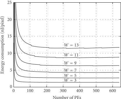
Figure 6shows curves of the total energy forN = 640 (the number of pixels in a VGA image line) with filter width as parameter. The curves in Figure 6 show that beyond a certain degree of parallelism the saving in energy is very
marginal. While the trend is the same, larger filter kernels benefit from increased number of PEs.
It should be noted that configurations with more pro-cessing elements (PEs) can handle increased throughput for the same algorithmic complexity. The increase is propor-tional toPsinceP≤Nand the filter kernels can be fully par-allelised over the pixels in an image line. The minimum num-ber of processing elements needed to meet the real-time con-straint is given byPmin= Calg×fpixel/ fmax, whereCalgis the
algorithmic complexity in number of instructions, fpixelthe
pixel rate, and fmaxthe maximum clock frequency of the
pro-cessing elements (PEs). The clock frequency of the PEs can be increased further by optimisation and pipelining. While optimisation for speed leads to larger PE sizes and increases computation energy dissipation, the impact of pipelining on the SIMD scaling needs to be investigated further.
When throughput comes in the picture, power dissipa-tion becomes a more convenient metric for comparison [16]. Figure 7shows the power dissipation versus the number of PEs with performance (Perf = Nops× fpixel) as parameter.
The curves start withPmincomputed for PEs designed to run
at fmax = 50 MHz. Increasing parallelism beyond Pmin
in-creases the chip cost (area) which has been traded for lower power dissipation through supply voltage and frequency scal-ing [17].
In Figure 8, the energy scaling factor is shown which has been used to generate the power dissipation curves of Figure 7. The energy scaling factor (6) has been derived from the CMOS propagation delay model given in [18]. The scal-ing factor starts with unity at the Pmin corresponding to a
given performance and decreases as the number of PEs in-creases. A threshold voltage of Vth =0.5 V and maximum
supply voltage ofVdd max=1.8 V have been assumed in the
plotted curves. To allow for noise margin, the lowest operat-ing voltage has been set toVdd min=Vth+ 0.2 V:
Eratio=
V
th+ (Pmin/P)2/3
Vdd max−Vth Vdd max
2
0.1 GOP
10 GOPs
20 GOPs
30 GOPs
0 100 200 300 400 500 600 700
Number of PEs 0
1 2 3 4 5 6 7 8 9 10
P
o
w
er
dissipation
(W
)
Figure7: Impact of voltage scaling on power dissipation.
5.2. SIMD area scaling
5.2.1. Scaling the linear processor array
Due to its regularity, the linear processor array (LPA) can be easily scaled according to the desired performance, cost, and power figures. Silicon area of the processor array can be given byAparray=P×APE, whereAPEis area of a single processing
element. The array area scales linearly with the number of processing elements (P).
5.2.2. Scaling the line memories
The size of on-chip line memories is dictated by the algo-rithm to be executed and is independent of the number of PEs used in the SIMD configuration. From area point of view, the line memories do not scale; they only change in lay-out shape since more pixels would be allocated per PE as the number of PEs decreases. The silicon area contribution of the line memories becomesAlmem=NlinesAline.
5.2.3. Scaling the global controller
Like the line memories, the global controller also does not scale with change in the number of PEs. This is to be expected since, in the SIMD principle, the global controller is already a shared resource by all PEs. The global controller area is sim-plyAgcon.
5.2.4. Scaling the program memory
The program memory scaling depends on how the impact of loop overhead is addressed. When there are fewer PEs than the number of pixels in a line, algorithms need to be iter-ated over partitions of an image line. The overhead is asso-ciated to the instructions that control the iterations and can be considerable when the loop body is small. A straightfor-ward way of reducing the loop overhead is to unroll the loop by replicating the algorithm code. This results in an increase in the program memory by an amount, that is, a function of the length of the unrolled code and the number of repli-cations. The area of the program memory can be given by
0.1 GOP 10 GOPs 20 GOPs 30 GOPs
0 100 200 300 400 500 600 700
Number of PEs 0.1
0.2 0.3 0.4 0.5 0.6 0.7 0.8 0.9 1
Energ
y
scaling
fact
or
Figure8: Energy scaling factor for varying computational demand.
Apmem = NopsNunroll(1 +γ)Ainstr, whereAinstr is the area of
a single instruction and γ is the increase factor related to address-width expansion. Instead, one can use special loop control hardware in the global controller to avoid the cost of replicating codes.
5.3. Scaling case study
To summarize the SIMD scaling issue, we collect the com-ponents into one cost function described in terms of silicon area:ASIMD=Aparray+Almem+Agcon+Apmem.Figure 9shows
how the SIMD area scales with the scaling in the number of PEs. The curves are offset by an amount equivalent to the line memory and global controller areas which do not scale. Since the size of the program memory is small relative to the other components, the relative impact of loop unrolling is minimal for large array sizes. For lower number of processing elements (P <200), the area of the nonscaling components dominates. Under this condition, it is sensible not to scale down the number PEs so that the performance loss in the no loop-unrolling case can be compensated for. When com-bined with the power scaling curves given earlier, the area scaling curve provides a quantitative means for performance-driven SIMD scaling.
6. CONCLUSIONS
In this paper, we have motivated the use of a scalable pro-grammable architecture for video processing in the various applications of smart cameras. It appears that the highly par-allel nature of image processing algorithms allows to put the major part of the load on an SIMD type of processors. An-other processor in the system has to be a general-purpose mi-crocontroller, microprocessor, or DSP.
No loop unrolling With loop unrolling
0 100 200 300 400 500 600
Number of PEs 0
5 10 15 20 25 30 35
Chip
ar
ea
(mm
2)
Figure9: SIMD area scaling based on a 0.18µm design data.
certain number of processors is used. The SIMD area in-crease is linear in the number of processors with an offset. For practical low-cost applications, a design at maximum sil-icon speed is preferred with a sufficient level of parallelism to obtain some power savings. When voltage scaling is used, the lowest power consumption for a given performance is achieved at the needed number of processors at the maxi-mum silicon speed of the IC at the lowest voltage supply.
REFERENCES
[1] J. C. Gealow and C. G. Sodini, “A pixel-parallel image proces-sor using logic pitch-matched to dynamic memory,”IEEE J. Solid-State Circuits, vol. 34, no. 6, pp. 831–839, 1999. [2] H. Yamashita and C. G. Sodini, “A 128×128 CMOS imager
with 4×128 bit-serial column-parallel PE array,” inProc. IEEE International Solid-State Circuits Conference Digest of Techni-cal Papers (ISSCC ’01), pp. 96–97, 436, San Francisco, Calif, USA, February 2001.
[3] A. A. Abbo and R. P. Kleihorst, “A programmable smart-camera architecture,” inProc. Advanced Concepts for Intelli-gent Vision Systems (ACIVS ’02), pp. 6–13, Ghent, Belgium, September 2002.
[4] R. P. Kleihorst, A. A. Abbo, A. van der Avoird, et al., “Xetal: A low-power high-performance smart camera processor,” in
Proc. IEEE Int. Symp. Circuits and Systems (ISCAS ’01), vol. 5, pp. 215–218, Sydney, New South Wales, Australia, May 2001. [5] T. H. Meng, “Wireless video systems,” inProc. IEEE Computer
Society Workshop on VLSI System Level Design, pp. 28–33, Or-lando, Fla, USA, April 1998.
[6] RoboCup, “The RoboCup web site,” 2002, http://www. robocup.org/.
[7] P. P. Jonker,Morphological Image Processing: Architecture and VLSI Design, Kluwer Academic, Amsterdam, the Netherlands, 1992.
[8] W. Caarls, P. P. Jonker, and H. Corporaal, “Data- and task par-allel image processing on a mixed SIMD-ILP platform using skeletons and asynchronous RPC,” inProc. 5th PROGRESS Seminar on Embedded Systems, pp. 27–34, Nieuwegein, the Netherlands, October 2004.
[9] P. P. Jonker, “Why linear arrays are better image processors,” inProc. 12th IAPR International Conference on Pattern Recog-nition, vol. 3, pp. 334–338, Jerusalem, Israel, October 1994. [10] D. W. Hammerstrom and D. P. Lulich, “Image processing
us-ing one-dimensional processor arrays,”Proc. IEEE, vol. 84, no. 7, pp. 1005–1018, 1996.
[11] R. P. Kleihorst, H. Broers, A. Abbo, et al., “An SIMD-VLIW smart camera architecture for real-time face recognition,” in
Abstracts of the SAFE & ProRISC/IEEE Workshops on Semicon-ductors, Circuits and Systems and Signal Processing, Veldhoven, the Netherlands, November 2003.
[12] Trimedia Technologies, “portfolio,” 2002, http://www. trimedia.com/.
[13] R. K. H. Fatemi, R. P. Kleihorst, H. Corporaal, and P. P. Jonker, “Real-time face recognition on a smart camera,” inProc. Ad-vanced Concepts for Intelligent Vision Systems (ACIVS ’03), pp. 222–227, Ghent, Belgium, September 2003.
[14] R. Manniesing, R. P. Kleihorst, A. van der Avoird, and E. Hendriks, “Power analysis of a general convolution algorithm mapped on a linear processor array,”Journal of VLSI Signal Processing, vol. 37, no. 1, pp. 5–19, 2004.
[15] R. P. Llopis and K. Goossens, “The Petrol approach to high-level power estimation,” inProc. International Symposium on Low Power Electronics and Design, pp. 130–132, Monterey, Calif, USA, August 1998.
[16] A. A. Abbo, R. P. Kleihorst, V. Choudhary, and L. Se-vat, “Power consumption of performance-scaled SIMD pro-cessors,” in Proc. 14th International Workshop Power and Timing Modeling, Optimization and Simulation (PATMOS ’04), vol. 3254, pp. 532–540, Santorini, Greece, September 2004.
[17] R. W. Brodersen, A. Chandrakasan, and S. Sheng, “Design techniques for portable systems,” inProc. IEEE 40th Interna-tional Solid-State Circuits Conference (ISSCC ’93), pp. 168– 169, San Francisco, Calif, USA, February 1993.
[18] S.-W. Sun and P. G. Y. Tsui, “Limitation of CMOS supply-voltage scaling by MOSFET threshold-supply-voltage variation,”
IEEE J. Solid-State Circuits, vol. 30, no. 8, pp. 947–949, 1995.
Richard P. Kleihorstreceived the M.S. and Ph.D. degrees in electrical engineering from Delft University of Technology, the Nether-lands, in 1989 and 1994, respectively. In 1989, he worked at the Philips Research Laboratories in Eindhoven, the Nether-lands, on fuzzy classification techniques for video-speed optical character recognition. From 1990 to 1994, he worked as a Research Assistant, investigating the application of
Anteneh A. Abboreceived his B.S. degree in electrical engineering from Addis Ababa University, Ethiopia, his M.S. degree in elec-tronic engineering from Eindhoven Univer-sity of Technology, and his Ph.D. degree from Delft University of Technology, the Netherlands. Since 1999, he has been work-ing at Philips Research Laboratory in Eind-hoven as a Senior Scientist. His research in-terests include signal processing architec-tures and IC design methodology.
Vishal Choudhary received his B.E. de-gree in electronics engineering from the S.G.G.S College of Engineering and Tech-nology, Nanded, India, and the M.Tech. de-gree in VLSI design tools and technology from the Indian Institute of Technology, New Delhi, India. Since 1999, he has been working as a Research Scientist in the Group Digital Design and Test, Philips Research Labs in Eindhoven, the Netherlands. His
re-search interests include dynamic power management for SoC, low power VLSI design, and reconfigurable computing architectures.
Harry Broersreceived the M.S. degree in electrical engineering from the University of Twente, the Netherlands, in 2000. In 2000, he started to work on image processing for industrial applications at the Philips Centre for Industrial Technology in Eindhoven, the Netherlands. He worked as a Research Sci-entist, investigating the application of ma-chine vision for assembly systems in the In-dustrial Vision Department. Since 2003, he