University of Twente
Faculty of Electrical Engineering,
Mathematics & Computer Science
Frequency Division
Fabian van Houwelingen MSc. Thesis
July 2006
0. Table of Contents
1. Preface...3
2. Introduction...4
3. Frequency divider concept...6
4. Voltage gain and frequency limitations ...10
4.1 Introduction...10
4.2 Transistor transit frequency ...10
4.3 Frequency limit on amplifier stages...11
4.4 Numerical example ...12
5. Implementing the discharge circuit...14
5.1 Introduction...14
5.2 Implementation suggestions and their limitations ...14
6. Delay...18
6.1 Introduction...18
6.2 The concept of delay as used for frequency division...18
6.3 Implementation of delay ...20
7. Superharmonic Injection Locking...24
7.1 Introduction...24
7.2 Definitions...24
7.3 Loop analysis ...25
7.5 First circuit implementation used for simulation ...31
7.6 Enlarging the locking range ...37
7.7 Final implementation of frequency divider design ...37
8 Phase Noise...44
8.1 Introduction...44
8.2 Time variant phase noise for a free running ring oscillator ...44
8.3 Simulation results...48
9. Divider Performance and Benchmarking...50
10. Conclusions...52
11. Appendix A...54
13. Appendix C ...62
14. Appendix D...64
1. Preface
This Master Thesis report summarizes the past 8 months of the last year of my study Electrical Engineering at the University of Twente. This master thesis has been an assignment which allowed a great deal of creativity; where on one hand everything should be exactly calculated, simulated, predicted and measured, on the other hand a form of creative and ‘free’ thinking may be necessary in order to find out whether or not it is ‘possible’ to create a certain circuit.
This creative process has been a very learnable experience for me. I would like to thank the people who supervised this project; Eric Klumerink and Bram Nauta. I also would like to thank the ICD group to allow me to do a chip-talk presentation about this subject; it yielded some very useful discussions. I also would like to thank Mustafa Acar for discussions regarding the overlap of static and dynamic frequency dividers and Ronan van der Zee, member of the graduation committee.
2. Introduction
In analog RF transceiver circuitry, several components are needed to receive and send signals modulated at a high frequency carrier. A stable frequency ‘generator’
(frequency synthesizer) is a very important building block in a transceiver circuit. This synthesizer should be capable of generating a periodic signal with a very stable and accurate frequency. This periodic signal can be used for instance in clock
recovery circuits or mixing stages. When the frequency synthesizer is implemented as a Phase Locked Loop (PLL), the scheme of the synthesizer looks as shown in figure 1.
Figure 1 General scheme of PLL circuit.
In this circuit, a very stable frequency generated by a crystal (indicated as XTAL) is used to generate a periodic signal. This periodic signal usually has a frequency in the order of 10-300 MHz. A PLL provides a way of multiplying this frequency with a fractional number. The output signal of the PLL is given by the Voltage Controlled Oscillator (VCO). The blocks “
M 1
” and “ N
1
” are frequency dividers (also called
prescalers) which divide the frequency of the incoming signal by an integer value M and N, respectively. The values for M and N define the output frequency off the PLL as
XTAL VCO
out f
N M f
f = = * (1)
For instance, when N = 1 and M = 10, the PLL output frequency is ten times higher than the reference crystal frequency. Because of the feedback loop, which consists of a phase comparator and a loop filter, the VCO is locked in phase to the crystal. This means that the VCO output signal has the frequency stability of the reference signal generated by the crystal. Basically a PLL is an effective way of creating a high frequency periodic signal having a stable and accurate frequency.
If the dividers used are programmable (i.e. the divisor number can be altered) the output signal of the PLL can have a programmable frequency. This report focuses on the frequency dividers. As mentioned before, the function of the divider is to divide the frequency of the incoming signal by an integer number. There are several parameters defining the overall performance of the frequency divider. These parameters are given below:
N
1
M
1
ϕ
Δ
=
K
*
V
outXTAL VCO
1. The power and blind current required from either the VCO or reference crystal driving it. This power is usually defined relative to 1 mW; the unit used for this parameter is dBmW. Because the reference crystal generally has a much lower output frequency than the VCO, the larger blind currents will have to be provided by the VCO. It is important that the required input blind power required does not exceed the capabilities of the VCO.
2. The frequency range at which the divider operates correctly (i.e. divides the frequency by the specified integer number). Different frequency divider topologies have different limits to this frequency range.
3. The maximum input frequency; this is a measure of the maximum speed of the frequency divider
4. The power consumption; i.e. the average current drawn from the power supply.
5. Phase noise at the output of the divider, and the way this phase noise depends on the input signal.
The value of every parameter depends on the type of frequency divider. There are two types of frequency dividers that can be defined:
1. Static Frequency dividers. These types of dividers employ a so called ‘toggle flip-flop’ or T flip-flop. This type of circuit has two states and ‘toggles’ between these states for every incoming low to high transition. This function is equivalent to frequency division by two. Because a T flip flop can keep its state indefinitely during absence of low to high transitions, it operates from all frequencies between DC and a maximum input frequency.
2. Dynamic frequency dividers. This type of dividers differs from the static type in the sense that a dynamic divider cannot maintain one state indefinitely in the absence of an input signal. This restriction implies that there is a minimum frequency as well as a maximum frequency at which the divider operates properly. Dynamic dividers can be divided into two categories; the first category is the so called “Regenerative” or “Miller” frequency divider [1], the second category is the so called “Injection Locked Frequency Divider” [2]. Because both types of dividers have minimum and maximum input frequency at which the divider works properly, the operating range is smaller than the range of a static divider.
3. Frequency divider concept
The initial goal of this project was to design a frequency divider, working at the highest possible speed that exploits the inherent speed of transistors to almost instantly convert an incoming gate voltage to a drain current. This voltage / current conversion is not limited to the transistor Unity Gain Frequency (or Transit Frequency ft), and therefore maybe the ft limit can be circumvented. The following conceptually
drawn circuit exploits this property.
Figure 1 Conceptual current source.
In this figure, the input of the circuit is the voltage source Vin(t) which is surrounded
by 4 transistors. Both PMOS and both NMOS transistors have equal dimensions. NMOS1 and PMOS1 form a CMOS inverter which has its output and input shorted. This way, the inverter is biased such that the drain current of PMOS1 is equal to the drain current of NMOS1. PMOS2 and NMOS2 also form an inverter, which is used as a current source. The output of the circuit is the current Iout(t). If Vin(t) is a binary
Return to Zero signal (i.e. Vin(t) is a square wave signal assuming only 2 voltages, one
of which is zero volts) the output current Iout(t) also is a binary Return to Zero signal.
The phase between Vin(t) and Iout(t) is zero and the output current is equal to
( )
m in t GV ⋅ regardless of the frequency of the input signal Vin(t) (Gm is the sum of the
average transconductances of PMOS2 and NMOS2). The output of the circuit can be connected to a capacitor, in this case Iout(t) (from now on called I1(t)) is used to charge
that capacitor. This is shown in the following figure, the capacitor is called Cint.
Figure 2 Current source, a capacitor and a discharge circuit.
A second circuit creates a current I2(t) that discharges the same capacitor Cint. For now
it is supposed that I2(t) is zero. In this case Vin(t) and VC(t) can be drawn as shown in
the following figure.
Iout(t)
- Vin(t) +
PMOS1 PMOS2
NMOS2 NMOS1
Discharge Circuit I2(t)
I1(t)
VC(t)
Figure 3 Input voltage and capacitor voltage in case of absence of I2(t).
As can be seen in figure 3 the circuit works as a fully linear integrator. If the PMOS2 and NMOS2 devices in figure 2 are modeled as ideal current sources (i.e. their output resistance is infinity and the output current is in phase with the input voltage) this integrator works at arbitrarily high frequencies. This linear integration is a way of creating a timer which ‘counts’ the amount of incoming periods (one period is shown in figure 3 as “Tin”). In order for this circuit to work as a frequency divider, the
following additional functions are needed:
• The voltage VC(t) should be compared to a reference voltage, this reference
voltage corresponds to an integer amound of periods n·Tin.
• When VC(t) exceeds this voltage, the capacitor should be discharged (this is a
way of resetting the timer). For this a current source generating the discharge current I2(t) is needed.
These two functions should be implemented in the “Discharge Circuit” as shown in figure 2. The frequency divider concept is based on the notion that transistors convert voltage into current in an almost infinitely fast way. In order for this concept to be useful, the final implementation of this discharge circuit should not form a speed limitation that is based on the transit frequency ft. Before the implementation of this
circuit is considered, the frequency divider concept will be shown by visualizing the signals VC(t), I1(t) and I2(t) in figure 4.
Vin(t)
VC(t)
0
t 0
V
V
t
Figure 4 Charging and discharging a capacitor in order to divide a frequency by 2. This chapter will only consider a frequency division ratio of 2 to keep the analysis simple. For the same reason a square wave input is considered instead of a sine wave (at high frequencies the output of a VCO is more likely to be a sinewave).
The discharge circuit has a transfer function VC(t) Î I2(t). In figure 4 however it is
seen that this transfer function is a very unsuitable function, if it has to work at high speeds (see the waveforms in figure 4). This transfer function implies:
• Infinitely fast switching between no current and a relatively large discharge current; conceptually an infinitely small voltage difference in Vc(t) at the input
of the discharge circuit should create a current difference of I2 at the output of that circuit. If a voltage controlled current source would be used to discharge the capacitor Cint, its transconductance should be equal to = =∞
Δ Δ =
0
2
I V
I g
C
m .
• Strong time variance; once the discharging starts, the current I2(t) should
remain high even though the input voltage falls at the same time. It would look as if a capable’ circuit could do this job. However, this ‘memory-capable’ circuit should then be capable of switching off I2 infinitely fast,
which causes the same amplification problem.
Maybe the discharge circuit would also work if the transconductance is less than infinity. However that means that the concept itself needs to change. Changes in this concept are made in chapter 5 such that the two ‘impossibilities’ mentioned here can be circumvented and indeed a finite gain suffices. However when making that change, it appears that the discharge circuit implementation will suffer from the ft speed
limitation. This process will be described in chapter 5, but first the speed limitation itself is discussed in chapter 4.
I1(t)
VC(t)
0
t 0
V
V
t
Tin
I2(t)
0
t V
Tout
4. Voltage gain and frequency limitations
4.1 Introduction
When CMOS implemented circuitry operates at very high frequencies, the ability of the transistors to amplify an incoming signal is limited. A well known property that illustrates this is the “transit frequency”, which is the frequency at which the current gain for a transistor is equal to 1, when its output is shorted. In this paragraph, the transconductance gm of a transistor is assumed a constant.
4.2 Transistor transit frequency
Figure 5 Circuit illustrating frequency limitation of transistors.
Consider the common source stage depicted in the figure above. The voltage at the gate of the transistor is given by:
( )
I( )
t Ct I
C
VG t ω
ω
ω 1 cos
sin 1
0
0 =−
=
∫
∞
− (2)
C is the total impedance seen at the gate (this mainly consists of the gate-source capacitance and the gate-drain capacitance). The gate-source voltage directly relates to the drain current as follows:
( )
t IC g g
V
I m
m G
out = * =−ω 0cosω (3)
When comparing the magnitudes (i.e. absolute values) of the incoming and outgoing currents, the current gain can be derived:
C g I I
A m
S out
ω =
= (4)
The frequency at which this current gain falls to 1 is given by the following equation:
↓
I
out( )
t IIS = 0sinω
C g f m t * 2π
= (6)
This frequency is referred to as the transit frequency. The next paragraph will use this expression for the transit frequency to evaluate the frequency limitation of common source amplifier stages.
4.3 Frequency limit on amplifier stages
Figure 6 Cascade of n common source stages.
This figure shows n cascaded common source stages (indexed as Qn), all of which
have 3 parameters. These parameters are input capacitance Cin, output resistance Rload
and tranconducance gm. All parameters are assumed constant and equal for every
stage. At what frequency does the stage Q(n-1) have unity voltage gain?
Q(n-2) has a certain output current. The current into the capacitance of Q(n-1) equals
)) 2 ( ( )) 1 (
( − 1 −
+
= out Qn
in out out n Q in I C j R R I ω (7)
This creates the following output current for Q(n-1):
in out out in n Q out m in n Q in m in m n Q out C j R R C j I g C j I g V g I ω ω
ω * * 1
*
* ( ( 1)) ( ( 2)) )) 1 ( ( + = = = − −
− (8)
In order for the voltage gain to equal 1, the absolute value of the incoming and outgoing current should be equal:
1 )) 1 ( ( )) 2 ( ( = − − n Q out n Q out I I (9) This implies:
( )
t VVS = 0sin ω
↑
I
SQ1 Q2 Q3 Q4 Qn
Rload
1 1
* =
+
in out
out in
m
C j R
R C
j g
ω
ω (10)
When isolating ω, the unity voltage gain frequency of a common source stage can be found:
out in
out m
R C
R g f
π 2
1
2
2 −
= (11)
When Rout is very high such that gm·Rout >>> 1, then this equation reduces to:
C g
f m
* 2π
= (12)
This is the transit frequency as previously described. However, the total Rout of a
common source stage is bound to a maximum value, due to several reasons. The first reason is the finite output resistance of the NMOS transistor. The following paragraph shows that the actual unity voltage gain frequency for cascaded amplifiers as shown in figure 6 is potentially far lower than the transit frequency of the transistor used.
4.4 Numerical example
In this example, equation (11) is evaluated for a single stage NMOS common source amplifier, which amplifies the incoming voltage such that the output voltage swing is large (i.e. is close to both supply rails). This example is important because when a ‘ring oscillator’ is built out of these types of amplifiers, the output voltage swing at each node of this oscillator will be this large. Chapter 5 describes that the actual implementation of the frequency divider is based on an oscillator, and therefore this numerical example will show what actual speed can be expected from a cascade of common source amplifiers.
In order to reach maximum speed, the channel length of the transistor will should be the minimum that the CMOS technology allows. In this case a 90 nm process will be considered with a minimum gate length of 0.1 μm. Numerical values for
transconductance, output resistance and capacitances are extracted using ProMOST.
In the CMOS090 process if a 2/0.1 NMOS is in the strong inversion, saturation region this channel output resistance is in the order 5kΩ − 10kΩ. In order for the NMOS transistor to have a sufficient transconductance, it needs a drain current. A simple model would describe that relation according to:
D ox n
m I
L W C
g = 2μ (13)
In the aforementioned 2/0.1 transistor, this averaged current has an order magnitude of 0.3mA, yielding a transconductance order 1.3 mS. The voltage across the transistor on average is assumed 0.6V. This means that in order for this current to flow into the transistor, the load resistance Rload should have a value in the order of 2 kΩ.
This however gives additional problems. If the transistor length is increased, its output resistance obviously increases, however the drain current decreases. This means that the PMOS has to be biased stronger (higher VDS and VGS). Numerical extraction from
ProMOST yields a drain current of 0.3mA using a 3/0.15 μm dimensioned transistor (its gate-source voltage set at the maximum supply voltage of 1.2V), which has an output resistance of 3.2 kΩ.
However there is a biasing problem; the minimum PMOS drain source voltage needed for this setting is 500 mV, leaving 700 mV of swing for the output voltage of one amplifier stage. This is unacceptable because, as assumed in the beginning of the analysis, the average drain source voltage of the NMOS is 0.6V and its output swing is large.
When the drain-source voltage of the PMOST decreases, both its drain current and output resistance decrease. Using a longer transistor channel length than 0.15 μm creates an insufficient drain current which can only be corrected by increasing the channel width (because the VGS bias is already at maximum). However when the
width of the channel is increased, the output resistance falls below 2 kΩ. Therefore a PMOS is not a sufficient option if large voltage swings are required.
This means that the product gm·Rout now has a magnitude of 2·1.3=2.6. However it
gets worse; because very large voltage swings are assumed (close to the supply voltage) there is a certain amount of time at which the input voltage to the NMOS is below the threshold voltage, lowering the average transconductance. When assuming 1.2 V of swing and a threshold voltage of 0.4V, the average transconductance that remains is 0.7 mS. This means that the product gm·Rout now has a magnitude of
2·0.7=1.4.
When using these values in (11) (R=2000; gm = 0.0007), the resulting frequency
would be
in
C e f
π * 3 4
1
= , while the transit frequency is
in t
C e f
π * 3 4 . 1
1
= . This means that the unity voltage gain of the system is about 0.4·ft, which is a 60 % loss in speed.
↑
I
2(t)
V
C(t)
C
gateÆ
I
1(t)
gm
5. Implementing the discharge circuit
5.1 Introduction
In this chapter, the design process of the discharge circuit will be described. As explained in chapter 3, the concept of frequency division using the charge in a capacitor as ‘the time information’ has inherent impossibilities. The goal of this chapter is to show that in order to circumvent these impossibilities an oscillatory circuit can be an effective implementation.
5.2 Implementation suggestions and their limitations
Figure 3 shows the total frequency divider. The discharge circuit (shown in figure 2) has an input signal which is the voltage across the capacitor VC(t). Its output signal is
the discharge current I2(t). The first design decision made is to keep the value of the
capacitor as small as possible, because if there are limitations on the amount of current available to charge and discharge the capacitor, higher voltage swings are possible. The first implementation idea assumes that Cint can be implemented as the
capacitance seen at the gate of a transistor.
Suppose the discharge circuit is implemented as a single transistor, having a constant transconductance gm and an input gate capacitange Cgate, which is drawn separately
from the transistor (see figure 7).
Figure 7 Conceptual implementation (left) simplified equivalent circuit (right)
Conceptually, this is just a 1-pole linear system that cannot generate any other
frequency than that has been put into it. Therefore it cannot be a frequency divider by itself (which has to ‘create’ a new frequency). The transconductance gm shown in
figure 6 could be nonlinear however that does not help; it will only create harmonics of the input signal (a frequency divider should create a ‘subharmonic’). An analysis of this circuit is given in Appendix A. This appendix shows that this circuit will work as a low pass filter when a square wave current is assumed to be the input.Suppose the circuit is modified as shown in figure 7.
Æ
I
2(t)
C
gateÆ
I
1(t)
Figure 8 Modified discharge circuit.
It now consists of a separate capacitor Cint (which could be made a lot smaller than a
transistor gate capacitance) and a separate transistor, used to discharge the capacitor. The separation element is a switch. The reason to separate the capacitor from the discharge transistor is to create a discharge current that is less dependant on VC(t); the
output impedance of the discharge current source has increased from 1/gm to Rout. If
the switch is implemented as a transistor, the circuit would look as shown in figure 8 (NMOS1 is the switch):
Figure 8 Switch implemented as NMOS (left) and redrawn (right)
This circuit is redrawn on the right part of figure 8.
Initially VC(t) = 0, NMOS1 is off, Va(t) = 0 and NMOS2 is in deep triode region.
When I1(t) charges Cint such that VC(t) is high enough to bring both transistors in
saturation region (which is the only way to discharge the capacitor Cint) the small
signal impedance seen the when looking into the drain of NMOS1 is equal to Rout2.
Although the current source has an increased output impedance (when compared to the previous case depicted in figure 7, where the impedance was 1/gm of the discharge
transistor), the total system is still a 1-pole system as described in appendix A and therefore it cannot be a frequency divider. The problem lies in the fact that the transfer between VC(t) and the switch state should be time variant.
↑
I
2(t)
V
C(t)
C
intÆ
I
1(t)
Rout+
V
DC↑
I
2(t)
C
intÆ
I
1(t)
Rout1
+
V
DCNMOS1
NMOS2
Va
(t)
VC
(t)
Æ
I
1(t)
C
intRout2
+
V
DCNMOS2
Va
(t)
state of switch voltage across the capacitor VC (t)
open closed 0
Vt
The behavior is shown in the following figure:
Figure 9 Switch transition voltages.
This is a time variant function; exceeding a certain voltage Vt ‘triggers’ a pulse with a
predetermined length (this pulse controls the switch). One circuit that has this
property is a monostable circuit, which will be discussed here. A mono-stable circuit creates a ‘high’ pulse with duration T2 when a ‘high’ pulse is applied to the input,
with duration T1 such that T2 does not depend on T1. An example of this circuit is
shown in figure 10.
Figure 10 Mono-stable circuit.
Analysis of this circuit is given in appendix B. The following important conclusions can be drawn from the analysis:
1. During the high output pulse, C1 has to charge. Because the time T2 depends
on how fast C1 charges and discharges, the minimum output pulse length is given by the current through C1 and the value of C1.
2. Because the current trough C1 when it charges is very small (because both N1 and N2 are off when this charging takes place) the minimum value of T2 is
very large, and would result in a low frequency divider input frequency. Because no solution which deals with this problem sufficiently has been found that would significantly shorten T2 while keeping the pulse duration T2
uncorrelated to the input pulse duration T1, it is chosen not to implement the frequency divider using a mono-stable circuit.
input
Vout
N1 N2 R3 N3
R4 R2
R1
C1 V1
6. Delay
6.1 Introduction
This chapter will describe why a delay is the more efficient way to implement the transfer from VC(t) to I2(t). The previous chapter has concluded that in order to
implement time variance in the form of a mono-stable circuit, the resulting output frequency will be very limited.
6.2 The concept of delay as used for frequency division
Now consider the case where the time variant function in the frequency divider is replaced by a pure delay. In this case, the concept of the charge / discharge model, that was initially defined in figure 4 has to undergo a change:
Figure 11 Delay incorporated into the charge / discharge concept.
As can be seen in this figure, when the signals -I1(t) and I2(t) are added and integrated
with respect to time, the signal shape that results roughly equals the shape of VC(t).
As will be shown later, the non-linearities in the implementation of this concept will create a stable state, in which exactly 1 period of I2(t) (which has a length of Tout)
contains a charge that is equal to the charge of 2 periods of I1(t) (which has a length of
Tin).
Because of implementing a delay between the input of the discharge circuit VC(t) and
the output I2(t) of the discharge circuit, there is one crucial change: The relation
I1(t)
VC(t)
0
t 0
V
V
t
Tin
I2(t)
0
t V
input
I2(t)
I1(t)
+
VC(t)
-delay
Vd(t)
Cint
between the input voltage VC(t) and the output current I2(t) has become less time
variant and more linear. This can be seen by evaluating the correlation between both signals in figure 11. I2(t) looks like VC(t) passed through a low pass filter. This creates
the possibility of omitting a time variant system like the mono-stable circuit shown in figure 10. The components needed when implementing a frequency divider based on a form of delay can be summarized as follows:
1. The Integration Capacitor Cint.
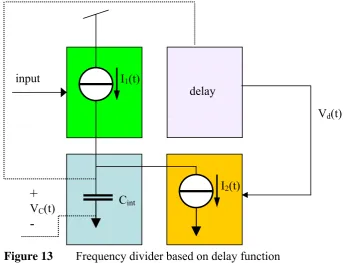
2. A current source which charges the capacitor. 3. A current source discharging the capacitor. 4. A form of delay.
5. A form of non-linearity that creates a stable condition; without this delay it is impossible to exactly match the current of both current sources. This non-linearity will be discussed in chapter 6.
The following figure will show the general scheme of such a frequency divider.
Figure 13 Frequency divider based on delay function
6.3 Implementation of delay
The delay concept as used in the general scheme has been put in a conceptual circuit shown below.
Figure 14 Delay implemented in frequency divider topology.
Figure 14 shows that the delay block is in between the capacitor and the discharge transistor. This paragraph supposes that in order for Cint to be as small as possible
(this is needed to ensure the highest possible speeds as discussed in § 5.2) the delay circuit inherently needs to be an active circuit. If only a passive R-C network would be used, the PMOS1 current source has to charge a significantly larger capacitor than when the delay block is implemented as an amplifier stage. In the latter case, Cint can
be a gate capacitance. If a passive solution would be used, the PMOS would have to drive a combination of capacitors and resistors. The following figure gives an example:
Figure 15 Delay implemented in a passive way.
The resistor / capacitor ladder consists of 2 resistors and 2 capacitors, but this is a fairly random choice. Whatever the implementation of the passive network is, VD(t)
inherently has a lower swing than VC(t) because current coming form the PMOS gets
wasted into an additional current path. This means that the current gain of NMOS1 needs to increase to make sure that I2 is still sufficiently large. However a larger
current gain means inherently a lower frequency, as was discussed in chapter 4. NMOS1
↑
I
2(t)
V
C(t)
C
intÆ
I
1(t)
Delay
V
in(t)
PMOS1
↑
I
2(t)
V
C(t)
C
intÆ
I
1(t)
V
in(t)
PMOS1
V
D(t)
Therefore, the ‘delay block’ shown in figure 14 has to be implemented in an ‘active way rather than a passive way. Figure 16 gives an example of an active
implementation.
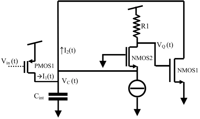
Figure 16 Delay implemented in an active way.
In figure 16 an active solution is presented, which means PMOS1 only has to drive
C-int in parallel to the resistance 1/gm of NMOS2. The delay is caused by a single
common gate amplifier stage, which has to drive the gate input capacitance of
NMOS1. VQ(t) is the voltage at the gate of NMOS1. However as simulations indicate,
this circuit assumes a state in which no frequency division takes place. The cause of this is that the linear behavior of this type of circuit dominates at high frequencies. It is very hard to find a full proof that states that for any size of the components shown in figure 16 and any input signal condition the linear behavior will prevail but various simulations show that at high frequencies the output voltage swings of an amplifier stage decrease. Circuit 16 contains 3 amplifier stages. Because all voltage swings decrease at very high frequencies, the transistor transconductances and output resistances will assume a ‘small signal’ value.
Therefore a linear analysis is given of the circuit of figure 16. Figure 17 shows a linear model of the circuit.
Figure 17 Linear analysis of the circuit shown in figure 16.
In this figure,
V
C,1(t)
is the voltage component caused by the current injection fromPMOS1:
↑
I
2(t)
V
C(t)
C
intÆ
I
1(t)
V
in(t)
PMOS1
NMOS1 NMOS2
V
Q(t)
R1
V
Q(t)
VC,2 (t)
VC,1(t)
int 1 , 1 , C V g
VC mPMOS in
ω ⋅
= (13)
Because the phase shift between Vin (see figure 16) and VC,1) is not relevant, it is
omitted in (13). The transfer function A can be written as
(
)
(
, 2)
, 12 , 2 , || 1 1 || 1 NMOS gate NMOS out NMOS out NMOS m C r R j r R g A ω +
= (14)
The transfer function B can be written as
int 1 , 1 , 1 ,
1 j r C
r g B NMOS out NMOS out NMOS m ω + = (15)
Both A and B are 1 pole low pass transfer functions. The following loop transfer function can be defined:
( )
( )
AB A t V t V C Q + = 1 (16)Where A and B are defined in (14) and (15). Because A and B are 1-pole functions, the product A·B can not assume the value -1 for any value of ω (that is, the phase shift caused by A·B will never reach π radians). This means that whatever the frequency of I1(t) is, the circuit of figure 16 will behave as a linear filter. The only
way to create a ‘new’ frequency (which might be an integer fractional of the input frequency), is to increase the total amount of poles around the loop such that the circuit behaves as a ring oscillator. It is known that if the stages in a ring oscillator suffer from an input capacitance minimum and an output resistance minimum (as was shown in chapter 4), the maximum output frequency of the circuit is only possible with the minimum number of stages. Therefore, it is chosen that the circuit given in figure 16 will be augmented with another amplifier stage within the loop such that a ring oscillator is created. In other words, the ‘delay’ block shown in figure 13 should be implemented as 2 amplifier stages.
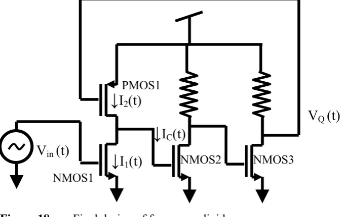
Because now 2 amplifier stages are used as the ‘delay’, the fastest possible option is to use 2 NMOS common source stages (each common source stage inverts the voltage, when a single stage was implemented like in figure 16, a common source could not be used for this reason).
One final design choice is made; instead of charging the capacitor using a PMOS, an NMOS will be used. The advantage of this is that the incoming voltage sinewave needs to provide less input power in order to create the same charge current I1(t),
because an NMOS has a larger current gain. It also appears that the locking range of the resulting divider is larger when an NMOS is used for the charging function (the mechanism for this will be explained later on in the report). Summarizing, the frequency divider now has the following aspects:
1. NMOS transistor is charging current source; 2. PMOS transistor is discharging current source;
Figure 18 Final design of frequency divider.
The capacitor Cint is actually the gate capacitance of NMOS2. This is because in
chapter 5 it was stated that the fastest way to implement the charge / discharge concept includes using the smallest possible capacitor. This circuit will behave as a ring oscillator, when taking into account the following aspects:
• The incoming periodic signal Vin(t) has a DC offset. The first reason for this is
that if there is a DC current flowing through NMOS1, then the voltage VQ(t)
will determine the direction of the current IC(t). This is because the product
VQ(t)·gm,PMOS1 can either be larger or smaller than I1(t) only if I1(t) is larger
than zero. The second reason for a relatively large DC current is that it increases both the transconductance of PMOS1 and of the NMOS1. • The loop gain of the circuit will be larger than 1 for the same frequency at
which oscillation occurs, as long as certain conditions regarding the transconductance, input capacitance and output resistance are met. These conditions are described in appendix C. The same appendix shows that for minimum length transistors, the maximum oscillation frequency lies in the region 15 GHz - 20 GHz and strongly depends on circuit parameters • The input voltage Vin(t) will not only be a DC bias; an AC voltage will be
superposed on the DC bias. The circuit’s own oscillation frequency will adjust such that it locks in phase to a subharmonic of this AC input signal by means of a non-linear mechanism. This creates a frequency divider which is generally referred to as an “Injection Locked Frequency Divider”.
The ring oscillator features non linearity in its transfer function. In contrast to the circuit shown in figure 16, this time the non-linearity becomes an important and dominant factor in the behavior of the circuit.
In this chapter the design, after evaluating certain potential possibilities for frequency division, it was decided to use a certain form of a ring oscillator, which allows
injection of an external signal into one of its transistors situated within the ‘ring’. This creates an injection current. This mechanism is a form of injection locking. Chapter 7 will describe the mechanics of injection locking using the non-linearity transfer function in the circuit, and why it is needed for frequency division.
V
in(t)
↓
I
1(t)
↓
I
2(t)
NMOS2 NMOS3
NMOS1
PMOS1
V
Q(t)
7. Superharmonic Injection Locking
7.1 Introduction
In order for a ring oscillator to work as a frequency divider, its oscillation frequency should track a subharmonic of the injected signal. This can happen if the nonlinearity in the oscillator is such that an intermodulation product of the injected signal and the oscillation already present creates this subharmonic. In order to explain the mechanics of this, a model is made of the circuit shown in figure 16 that incorporates:
• The linear transfer function consisting of a linear gain factor and a lowpass filter;
• The non-linearity that creates amplitude stability and enables the needed intermodulation;
• A node where the incoming current is ‘injected’ into a certain node of the oscillator.
The subsequent analysis presumes a division ratio of 2. This chapter will show that this division ratio provides a ‘locking range’ (i.e. the frequency range over which the injection locked divider works properly) which is large enough to overcome CMOS production process variations, but for this a nontrivial modification has to be made to the circuit initially proposed in figure 18.
7.2 Definitions
In order to keep the analysis simple, all present linearity is merged into one non-linear transfer function. This creates the model as shown in figure 19.
Figure 19 Scheme used to describe the superharmonic injection locking mechanism.
In this schematic, the green block represents the voltage controlled current source, which creates the injected current according to
IB(t)
IA(t)
(
)(
)
3 3 2 2 3 2 3 2 1 1 ) ( C R j C R j G G R R
H m m
ω
ω
ω
+ + =( )
(
)
∑
∞( )
= ⋅ = 1 1 1 n n n V ta t V f in m in A V G
I = * _
1
* m out B V G
I =−
+
C1 R1
+ V1(t)
-
+ Vout(t)
- +
Vin(t)
( )
in( )
m in A t V t GI = ⋅ _ (17)
The input voltage Vin is defined as
( )
t =Vξ(
ω t+ϕ)
Vin cos in (18)
where Vξ is the amplitude of the incoming voltage and ωin is the angular frequency of
the input signal.
The orange block is also a voltage controlled current source, which creates the following current:
( )
out( )
m1 B t V t GI =− ⋅ (19)
The voltage driving this current source is the actual output voltage of the divider which is defined as
( )
t V( )
tVout = ψ cosωos (20)
where Vψ is the amplitude of the output voltage of the ring oscillator and ωos is the
angular frequency of the output signal. The output voltage is considered the voltage at node 3 of the ring oscillator (see figure 18). In that figure this voltage is called VQ(t).
7.3 Loop analysis
In this paragraph it is calculated how the signals travel though the loop consisting of a non-linear and a linear transfer function. The voltage at node 1 is given by:
( )
(
( )
( )
)
11 t I t I t Z
V = A + B ⋅ (21)
Z1 is the impedance seen at node 1 of the ring oscillator and is given by:
1 1
1 1
1 = +
C R j Z
ω (22)
The voltage V1(t) is now subjected to the nonlinearity block which has the following
transfer function:
( )
(
)
( )
( )
( )
∑
∞( )
= ⋅ = ⋅ + + ⋅ + ⋅ + = 1 1 1 2 1 2 1 1 0 1 ... n n n nn V t a V t
a t V a t V a a t V
f (23)
When substituting for V1, this output can be written as
( )
(
)
(
(
( )
( )
)
)
(
(
( )
( )
)
)
nn m out in m in n n n B A
n I t I t Z a V t G V t G Z
a t
V
f
∑
∑
∞ = ∞ = ⋅ ⋅ − ⋅ ⋅ = ⋅ + ⋅ =
1 _ 1 1
1 1
1
It can be proven the output of the nonlinear transfer function can be written as the sum of all possible intermodulation products and harmonics. This proof is given by [4].
( )
(
V t)
Z K G V(
m t m) ( )
G V(
n t)
f os n n n n m in m m n m n m m in
m_ ξ cos ω ϕ 1 1 ψ cos ω
0 0
, 1
1 =
∑∑
+ ⋅ −∞
= ∞
=
+ (25)
Km,n is the 2-dimensional array of coefficients corresponding to these products. The
only intermodulation product that will be discussed further on is Vin(t)·Vout(t), which
has the coefficient K1,1. There are two reasons for this. The first reason is that this
simplifies the calculations; the second reason is that this product is very dominant in the behavior of the circuit. Higher order harmonics are assumed to be filtered out due to the low-pass characteristic of the ring oscillator. Furthermore, the intermodulation coefficients Km,n are considered constant (i.e. non-dependant on the nature of the
(
)
( )
(
)
(
)
⎟ ⎠ ⎞ ⎜ ⎝ ⎛ + − + + + − = ⋅ + − t t t t V V G G Z K t t V V G G Z K os in os in m in m os in m in m ω ϕ ω ω ϕ ω ω ϕ ω ψ ξ ψ ξ cos 2 1 cos 2 1 cos cos 1 _ 2 1 1 , 1 1 _ 2 1 1 , 1 (26)During locking at a frequency division ratio of 2, ωinj- ωosc = ωosc holds. The
frequency component ωinj+ ωosc will be filtered out as well, which means the total
voltage at a frequency of ωosc is equal to the ‘existing’ oscillation voltage added to the
intermodulation product K1,1:
( )
(
V t)
=−K ZG Vψ( )
ω t − K Z G G VξVψ(
ω t+ϕ)
f m os m in m cos os
2 1
cos 2 _ 1
1 1 , 1 1 1 1 , 0
1 (27)
This voltage can also be written as
( )
(
V t)
=−ZG Vψ(
K( )
ω t −K T(
ω t+ϕ)
)
f 1 1 m1 0,1cos os 1,1 cos os (28) where
2
_ 1G Vξ Z
T = m in (29)
This voltage designated f
(
V1( )
t)
passes through the second order linear low-passfilter, which has the following transfer function:
( ) (
2 2)(
3 3)
3 2 3 2
1
1 j RC j RC R R G G H osc osc m m ω ω ω + + = (30)
The output of this 2-pole transfer function (which actually is the implementation of the “delay” block as described in chapter 6) is the output voltage of the divider Vout:
( ) (
+ ω)(
+ ω)
ψ(
( )
ω +(
ω +ϕ)
)
−= ZG V K t K T t
C R j C R j R R G G t
V m os os
osc osc
m m
out cos cos
1
1 1 1 0,1 1,1
3 3 2 2 3 2 3 2
Z1 is the impedance consisting of R1 parallel C1:
(
1 1)
1
1 j RC R
os ω
+ (32)
Substituting for Z1 and for Vout(t) gives the following equation:
( )
(
( )
ω(
ω ϕ)
)
ω ω ψ ψ ⎟⎟⋅ + + ⎠ ⎞ ⎜⎜ ⎝ ⎛ + − =∏
= t T K t K V C R j R G tV os os
n os n n n mn
os cos cos
1
cos 3 0,1 1,1
1
(33)
This equation provides the operating conditions for superharmonic locking, in case of a frequency division ratio of 2. This equation provides two important boundary conditions; both sides contain a sinusoidal signal with a certain amplitude and phase. Both the magnitude and phase on either side of the equation should match in order to support injection locking. The foregoing assumptions are also applied here, stating that K0,1 and K1,1 are constant (this assumption will be revisited later). In this case, the
equation is a completely linear transfer function. This allows replacing the cosine functions with complex exponentials:
(
)
(
(
ω)
(
(
ω)
( )
ϕ)
)
ω
ω ψ
ψ V K j t K T j t j
C R j R G t j
V os os
n os n n n mn
os exp exp exp
1
exp 3 0,1 1,1
1 ⋅ + ⋅ ⎟⎟ ⎠ ⎞ ⎜⎜ ⎝ ⎛ + − =
∏
=This equation is generally being referred to as the ‘oscillation condition’ in literature. Dividing both sides by the term Vψ exp
(
jωost)
gives( )
(
ϕ)
(
( )
ϕ)
(
( )
ϕ)
ω sin cos exp 1 1 , 1 1 , 1 1 , 0 1 , 1 1 , 0 3 1 T jK T K K j T K K R G C R jn mn n n n
os = + = + +
⎟⎟ ⎠ ⎞ ⎜⎜ ⎝ ⎛ + −
∏
=This paragraph will utilize a strong simplification in order to evaluate the mechanics of injection locking. The simplification comes down to the following assumption:
C C C
C1 = 2 = 3 = (36)
R R R
R1= 2 = 3= (37)
m m m
m G G G
G1= 2= 3= (38)
These assumptions will simplify the oscillation condition and are justified by the notion that the order of magnitude of all the C, R and Gm values is the same, and in
the final design this is indeed the case. When using this assumption, the left hand side of (35) can be written as a complex number:
2 3 3 2 3 3 3 2 2 2 3 1 3 1 3 1 R G C C R j R G C R R G C R j m os os m os n mn n
n n
os ω ω ω
ω = − + − ⎟⎟ ⎠ ⎞ ⎜⎜ ⎝ ⎛ + −
∏
= (39)When equating both the imaginary and real parts, the following phase relation and gain relation for injection locking are found:
( )
(
ϕ)
ω ω sin 3 1 , 1 2 3 3 2 3 T K R G C C R m osos − = (phase relation) (40)
( )
(
ϕ)
ω cos 1 3 1 , 1 1 , 0 3 3 2 2 2 T K K R G C R mos − = + (gain relation) (41)
When one of these two conditions is not met, the circuit will not behave as a frequency divider. The natural oscillation frequency of a 3-stage ring oscillator is defined as (Appendix C):
RC
3
0 =
ω (42)
When substituting this value into the phase relation we find thatϕ=0which means that injecting a frequency
RC
in
3 2 =
ω creates an output signal Vout(t) which is exactly in
phase with the input signal Vin(t). Furthermore at the natural oscillation frequencyω0,
the left hand part of the gain relation equals 1 when GmRis equal to 2. This corresponds to a linear ring oscillator (appendix C).
The next paragraph will show how the phase condition can be met over a certain range of frequencies.
Analysis on the phase condition
In this paragraph, the phase condition will be analyzed further. Simulations will be used to support the analysis. Until stated otherwise, the ‘nominal’ C090 model library will be used the simulator (i.e. the library that represents the median outcome in the waver–to–wafer process mismatch) First the phase relation will be rewritten. Substituting for T in (40) gives
( )
ϕ ωω ξ sin
2 3 1 _ 1,1 2
3 3 2
3 ZG V K
R G
C C
R m in
m os
os − = (43)
( )
ϕ1 2 3 2 2 3 1 , 1 _ 1 3 2 3 ≤ − R G K V G Z C C R m in m os os ξ ω ω (44)
That is, when (44) holds, there will be a value of ϕ at which (43) holds. A few important remarks can made about this phase relation:
• When the injection current is increased (by increasing Gm-in or Vξ) the locking
range increases (the denominator in the left hand part of (44) increases). • When the intermodulation product K1,1 increases (i.e. if there is more second
order non-linearity) the locking range increases. This can be explained by stating that the circuit actually locks onto a subharmonic of the input frequency. The power of this subharmonic depends on the amount of intermodulation.
• When C or R decreases, the numerator decreases, enhancing the locking range. This can be explained by stating that when the RC-product seen at a node in the oscillator increases, its phase shift increases.
• When Gm increases the locking range also increases.
Now the shape of (44) will be provided giving the following assumptions (these assumptions are not accurate, but will provide a qualitative estimate)
• Vξis the input voltage amplitude to the frequency divider, which is 350 mV. • Gm_inis the transconductance of the current source (which is implemented as a
transistor). This transconductance depends biasing conditions (transistor gate, drain and source voltages). Using Appendix C, a transconductance of 0.8 mS is estimated for each stage.
• Z1is defined by (22) and is a 1-pole low pass transfer function, which
transforms the injected currentIB
( )
t into the voltageVB( )
t =Z1⋅IB( )
t . Only theabsolute value of this functionZ1gives the relevant information. When assuming an oscillation frequency ωos = 15 GHz, C = 4 fF and R = 4 kΩ
(estimated in appendix C), Z1 is in the order of 3500 Ω.
• The last unknown of the left part of (44) is K1,1. It is given in Appendix D that
2 1 , 1 2a
K = where a2is defined in the nonlinear function:
( )
(
)
∑
∞( )
= ⋅ = 1 1 1 n n n V ta t
V
f (45)
Because of the time-variant and voltage swing dependant nature of the
nonlinearity, an empirical approach is used to derive a value for a2. In order to
derive a2, the nonlinear transfer function block as given in figure 19 is driven
by a pure sinewave input. The harmonic distortion at the output of this block is then evaluated, and from the result a2 is extracted.
Figure 20 Input and output spectra used to derive a value for a2
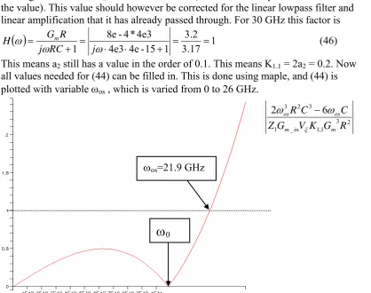
This figure shows that a2 has the order of 0.1 (the 30 GHz component is about 10% of
the value). This value should however be corrected for the linear lowpass filter and linear amplification that it has already passed through. For 30 GHz this factor is
( )
117 . 3
2 . 3 1 15 -e 4 3 e 4
3 e 4 * 4 -e 8
1= ⋅ ⋅ + = =
+ =
ω ω
ω
j RC
j R G
H m (46)
This means a2 still has a value in the order of 0.1. This means K1.1 = 2a2 = 0.2. Now
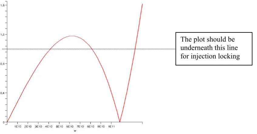
all values needed for (44) can be filled in. This is done using maple, and (44) is plotted with variable ωos , which is varied from 0 to 26 GHz.
Figure 21 A plot of the left hand side of (44) with ωos as variable.
input spectrum
output spectrum
ω
02 3 1 , 1 _ 1
3 2
3 6
2
R G K V G Z
C C
R
m in
m
os os
ξ ω
ω −
It can be seen that this plot exceeds the value 1 for a certain frequency . In this plot this is roughly 21.9 GHz, and because the value of (44) cannot exceed 1, injection locking will fail above an input frequency of 43.7 GHz. The locking range
corresponding to only the demands of the phase equation is called “phase limited locking range”. Because the ringoscillator only creates large phase shifts around its loop for frequencies above its natural oscillation frequency (which is indicated in the plot with an arrow), the phase equation will only provide a high frequency limit, not a low frequency limit. This is in contrast with injection locked LC-tank based
oscillators [5] which have symmetrical phase shift on either side of the natural oscillation frequency.
It should be noted that the plot in figure 21 is a very rough estimate and can only be used for qualitative analysis. If for instance the transconductance Gm is not 0.8 but if it
is 0.7, the graph of figure 21 will drastically change due to the fact that the numerator of the phase relation contains a factor Gm3. In addition to this, the modeled output
resistance and non linearities of every stage are also very rough estimates (R varies orders of magnetude depending on biasing conditions and only second order
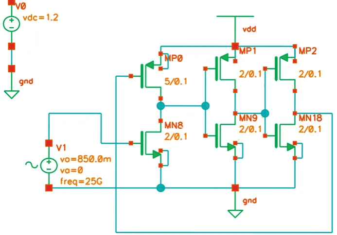
7.5 First circuit implementation used for simulation
The first simulation will treat the following implementation of the frequency divider.
Figure 22 Version of injection locked frequency divider used for phase analysis.
This implementation is different from the one shown in figure 18. The reason this implementation is used, because the circuit is ‘representative’ for the model
discussed. A few arguments (based on the analysis discussed in this chapter) suggest that this type of implementation is more suitable to verify outcome of the theoretical analysis. These arguments are described below.
1. When the oscillator runs freely, the voltage swings at the nodes should be large (i.e. close to the supply voltage range). This creates nonlinearity (a ‘clipping sinewave features harmonics). The nonlinearity is needed, because the higher the intermodulation coefficient K1,1, the higher the locking range
will be according to (44) Because initially it is assumed a that a PMOS device more effectively pulls a node voltage up to VDD, the resistors in figure 18 are
replaced with MP1 and MP2 in figure 22.
2. Furthermore, the resulting voltages at the nodes should not have the form of a squarewave. The reason for this is that a squarewave does not have even harmonics, i.e. the second harmonic coefficient a2 will be theoretically zero.
Because a2 is the most important coefficient for division by two, the
waveforms at the nodes of the oscillator should not approximate square waves. In order to achieve that it is chosen that NMOS and PMOS transistor sizes are equal (MP1, MP2, MN9 and MN18 of figure 22 are all 2/0.1 μm sized
transistors). Because in this way the gm of the NMOS devices will be higher
than the gm of the PMOS devices, the voltage waveforms at the nodes will
is made sure that the second order harmonic coefficient a2 is sufficiently
present. This was seen in the spectrum plot of figure 20.
3. Because of the strong biasing of MN8 at its gate (VGS = 0.85 V) MP0 has a
relatively large W/L ratio (5/0.1) to make sure that MN8 does not pull down the voltage at its drain too much; a second reason for this is to allow MP8 to pass a relatively average high drain current to accommodate a good
transconductance for MN8 (this is needed to maximize the ‘injection efficiency’ as defined by T in (29)
4. It is also assumed at this point that very high voltage swings at each oscillator node will make the circuit behavior less dependant on the injected current (i.e. the waveforms at each node are less dictated by the injected signal then by the circuit itself); if a relatively ‘constant’ nonlinearity and transconductance can be assumed these parameters are more predictable (Gm, Rand C are predicted
in appendix C). This is also achieved by creating large voltage swings.
Based on these arguments, the decision is made to initially use the circuit of figure 22 for simulation. The following simulation plots are made using the Cadence Spectre circuit simulator and a CMOS 090 model library. The output frequency is extracted from the ‘third node’ of the frequency divider, which is defined as the drain of MP18 and MN2 shown in figure 22. The reason for this is that the injected component (at double the oscillation frequency) is filtered out most at this node (due to the low pass filter present in every stage) and thus in the signal of this node, the relative power of ωos is the largest.
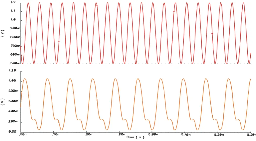
The circuit of figure 22 will now be simulated to find the locking range.
Figure 23 Divider operation at 29.03 GHz (top plot is the input, bottom plot is output)
43.7 GHz), but as stated before a minor estimation error in Gm can already make this
difference.
Important in this plot is that at the highest possible input and output frequency of the circuit shown in figure 22, the voltage swings are still very high (almost the complete supply voltage).
When slightly increasing the frequency to 29.05 GHz (which is exceeds the locking range limit by 20 MHz) using the same input amplitude of 700 mV peak to peak, the resulting behavior will be as shown in figure 24. The very low frequency component seen in the bottom plot of that figure (which is the output voltage) is called the ‘Beat Frequency’, and it is a product of a mechanism called “Injection Pulling” [5].
Injection Pulling occurs just outside the phase limited locking range.
In order to visualize the low frequency beat frequency, the scale of the horizontal axis of figure 24 is different from the scale used in figure 25. Both plots are simulations on the circuit shown in figure 22.
Figure 24 Injection pulling at 29.05 GHz (input is the top plot, output is bottom plot).
It is interesting to compare figures 23 and 25. The orange output plots of both figures show that the output signal lags in phase with respect to the injected sinewave when the oscillation frequency under injection is higher than the natural frequency ω0. The
opposite happens when the oscillation frequency under injection is lower than ω0. The
phase lag can be made clearer by showing a plot at which the injected frequency is exactly two times the oscillation frequency, which in case of the dimensions chosen in figure 22 is equal to 12.86 GHz. This plot is given in figure 26. It can be seen here that the ‘nod’ of the waveform appears in the center of the voltage swing (which corresponds to a summation of two sinewaves, at frequencies f and 2f, of which the zero transitions coincide), rather than above or underneath the center. This indicates that the intermodulation product which appears at the angular frequency ωos is in
phase with the free-running voltage ω0.
Figure 26 Output of divider at input frequency 2*ω0, both ωin and ωos are in phase.
The reason the locking range of the divider shown in figure 22 is only 5.6 GHz can be explained by assuming that estimates some of the parameters used to fill out (44) are inaccurate. The following plot is exactly like the one shown in figure 21, but this time only Gm is decreased slightly (Gm=0.6 mS).
Figure 27 Plot of left hand part of (44) with modified Gm.
7.6 Enlarging the locking range
In this paragraph an implementation of the frequency divider will be described, that has a larger locking range without using a higher injection voltage (in the entire report, an injection voltage of 700 mV peak to peak is used). It could be seen from the phase relation (44) that the injection power has to increase when the resulting output frequency of the frequency divider deviates more from its natural oscillation
frequency. That is, the more distance there is between the natural oscillation
frequency and the intermodulation product (which is at the input frequency divided by two) the more injection power is needed to ‘push’ the oscillator to a lower or higher frequency than its natural frequency.
In this paragraph a way is proposed to make the “natural oscillation frequency” dependant on the frequency of the injected signal.
It is known from chapter 4 that the ‘frequency at unity voltage gain’ of an amplifier stage (when it is placed in a cascade of amplifiers as shown in figure 6) depends on the transistor transconductance, its output resistance and its input capacitance. All three of those parameters depend on the biasing conditions of the transistor.
If these biasing conditions (i.e. the DC component of the voltages on each ring oscillator node) can be made dependant of the frequency of the input signal, the natural free running oscillation frequency ω0 of the divider would ‘shift’ to a different
value. Conceptually, a form of ‘frequency detection’ has to be implemented to
achieve this. An incoming frequency should be ‘converted’ to a certain DC voltage on one or more ring oscillator nodes.
There is a way to achieve this goal; consider the case where the voltage swings at the oscillator nodes during free running oscillation are small and at the same time lie close to one of the supply rails. An example in the case of a 1.2 V supply would be a voltage, having a DC component of 900 mV and an AC amplitude of 300 mV (which means the voltage swings between 1.2 V and 0.6 V). Increasing the amplitude of the AC component of that voltage will make the voltage ‘clip’ at the top side against the supply rail of 1.2 V, but it does not clip at the bottom side. This means that the DC component of the voltage has shifted.
The key idea is that the injected signal frequency controls the amplitude of those voltage swings. This is because a higher input frequency will be attenuated stronger in the loop, which as a 3rd order low pass filter transfer function. The next paragraph will explain how this idea can be implemented in the frequency divider, which initially looked as shown in figure 22.
7.7 Final implementation of frequency divider design
The implementation process starts out with the idea that at least one of the node voltages of the oscillator has to be close to the supply rails. This can be achieved by creating an ‘asymmetrical’ oscillator. Asymmetrical means that at a certain node for instance the NMOS transistor has a higher transconductance than the PMOS
it gets pulled to VDD. However when doing this the problem arises that the next stage
will amplify this “low” voltage to a “very high” voltage, which might clip entirely against VDD and therefore kill the AC component of the signal. The actual asymmetry
as implemented in the final divider has been chosen such, that the asymmetry itself is maximum while the circuit still oscillates when no injection power is present. The circuit is shown in figure 28.
Figure 28 Modified and final version of frequency divider shown in figure 22.
In this circuit, the NMOS1 has been made larger than MN8 in figure 22 while keeping the size of PMOS1 equal to the size of MP0 in figure 22. This results in a ‘low’ DC voltage at node 1. This ‘moderately low’ voltage is then amplified by the second stage such that at node 2 a ‘high’ DC voltage emerges. This is also the reason that in figure 22 a PMOS transistor is used; it is capable of pulling up the voltage at node 2 more than a resistor is. The size of the PMOS is relatively slow however. This is due to a speed optimization (when increasing the PMOS size, the overall gm/C ratio of that
stage decreases, which decreases the maximum input frequency). The last stage will amplify the ‘high’ voltage at node 2 to a ‘very low’ voltage at node 3. Because this voltage is applied only to PMOS1, and also a high voltage is applied to NMOS1, the voltage at node 1 will be pulled by NMOS1 and PMOS1 at rougly equal rates (which created the ‘moderately low’ DC voltage bias at node 1). Because the job of the 3rd stage is always to pull down the voltage at node 3, a resistor is used in that current path instead of a PMOS (which is a faster implementation). NMOS3 is pretty strongly biased, its gate source voltage is high, and the low value resistor allows a relatively large drain current. This means the transconductance of NMOS3 is high enough to drive the relatively large input capacitance of PMOS1, which forms the load of the 3rd stage. The resulting voltages are shown in the following figure.
Node 3
Node 2
Figure 29 The free running oscillation voltages of the circuit shown in figure 28.
It can be seen that the three nodes are now at different bias levels. The green plot of figure 29 belongs to the node where the injected current is added to the oscillation current. The colors of the plots will be used in the subsequent plots as well (orange is node 2, green is node 1 and blue is node 3). The natural oscillation frequency of the system is 16.06 GHz, this is higher than the 12.34 GHz of the circuit shown in figure 22. This has to do with the higher gm/C ratios in the second and third stage (1 less
PMOS transistor, the other is half the size compared to figure 22).
When the actual voltages at the nodes are studied carefully, it is found that the circuit biased itself such that the transconductance of each transistor is optimum. The transistor names of figure 28 are used here. The following biasing conditions appear:
• NMOS3 has a high DC bias gate source voltage. Its drain-source vo