o
-c
-~
____ . ___
==c~r~~r~.~~~~~~',
-.1
SL
FP
U
--f-bus
iu-data
... r- -,
....
,II
data
Hit :t 32
iu~adr ,
~
..
84
IU
c-tag "" ... -, 1/I
4i8
1 20
1
8
~~-c~ch. ·:h t4 / t.lg sram ~ ' - - - .
--~
84
C~J
K
. . .
-l1J
n::
u
~
U
I
qt CI)====
ea::
r£I
~ ~:::>
CO
I
~ CJ)-a
ab-va,
;
.
p-g,CD
...
..
~ H
fIljlll r
-N
~ ~
M ' -~'
...
~ flIN, ~ H
,
~jIIICD E--
----~ '"", ab~dataT
I I84
DMA
?
~
I
SCSII
ENETI
53C90 7990
I
1J
r - - -
j
scc85C30
i
W
J~-7 ' PROM
27C020
lI!IIIu-atat
I
-J
~
7 ' DSC
qt 79C30
ab-pa
"i CI)
j
~OD/NVRAMr-~
-
48~O2io~dat.
,It
Iab-va
ab-pa
~
-,
1
~1
,
84
84
84
RAM
RAM
VIDEO
1
I'I
I ~
U
I ~U
~12~
81
I
DRAMI
DRAM1M X 36 1M X 36
1
i
i
D
c
1. Introduction
SPARCstation-l Programmer's Modei
Stephen A. Chessin
DRAFT 7 Version 83, 89~lO
This paper describes the programmer's view of SPARCstation-l: address spaces, caching and
memory management, and interrupt levels. It is a synthesis of information contained in the hardware
specifications, but organized to be useful to a programmer.
Where appropriate, comparisons with the ustandard" Sun4 architecture are made.
WARNING: This document is a DRAFr and may contaiJi errors. Please report all mistakes to the author for correction.
Major Changes Since Draft 1 (Version L7)
(1) The page size has changed from 8K to 4IC.
(2) The size of a physical ~ bas changed from 29 bits to 28 bits.
(3) The Sbus has DlOved frooi Type 0 space to Type 1 space, and there has been a major reorganization of the Type 1 addresses to accommodate this. .
Cbanges Since Draft 2 (VersiOD 2.4)
'4) Minor typographical and editorial changes.
\3) Better explanations.
Changes Since Draft 3 (Version 3.7)
(6) The Intenupt Register is used to clear level 15 interrupts. (7) All Sbus devices are now desaibed using relative offsets.
(8) More bits are used in the Auxiliary InPUtlOutput Register. (Which used to be the Auxiliary Output Register.)
Changes Since Draft 4 (Version 4.7)
(9) The interrupt levels have been changed slightly. All Sbus devices, including the builtin ones,
inter-rupt on Sbus IRQ levels only.
(10) The Auxiliary Input/Output Register bas changed slightly.
(11) The definition of the DMA Write bit
was
backwards. (12) The video subsystem is off the board. again.Changes ~ince Draft 5 (Version 5.6)
Better explanations and addition of more examples.
Changes Since Draft 6 (Version 6.1)
(1) Added warnings that this is still a DRAFr document and may not be completely accurate.
(2) Described the bugs in various levels of hardware:
Synchronous parity errors cause asynchronous trapS (fixed in PI.7) SER records asynchronous errors (won't be fixed)
ASER and ASEV AR latch on synchronous memory errors (won't be fixed)
ASER sometimes isn't set on asynchronous errors (won't be fixed) ASEV AR isn't properly sign-extcnded on DVMA errors (won't be fixed) (3) Audio/ISDN replaces Audio DAC.
(4) Level 8 interrupts can be masked.
(5) Video goes into slot 3.
(6) Sbus IRQ6 and IRQ7 now map to SPARC level 8 and 9, instead of9 and 13. respectively.
(7) Miscellaneous corrections.
1. Address Spaces
The SP ARC Architecture defines the existence of at least 4 address spaces. A given implementation
may define mo-e than 4 address spaces. Selection of a particular address space is done via the Address
Space Indicator (ASI) field of the load and store alternate address space instructions. Ordinary load and
stole instructions automatica11y go to User or Supervisor Data space. depending upon the mode of the CPU.
Instruction fetches by the CPU automatically go to User or Supervisor Instruction ~ again depending upon the mode of the CPU.
The following table describes the address spaces defined by the Sun4 Architecture and the
SP ARCstation-l implementation.
ASI Sun4 Use SP ARCstation-l Use Comments
0x0 Reserved Reserved
Oxl
Restzved Reserved0x2 System Space Same Note 1
0x3 Segment Map Same
Ox4 Page Map Same
~ BIoctCopy Reserved Note 2
t>x6 Region Map Reserved Note 2 Ox7 Flush Cache (Regioo) Reserved Note 2 0x8 User Instruction Same
0x9 Supervisor Instruction Same 0xA User Data Same 0xB Supervisor Data Same
0xC Flush Cache (Segment) Same 0xD Flush Cache (Page) Same 0xE Flush Cache (Context) Same
0xF Flush Cache (User) Reserved Note 3 OxiO Flush I-Cache (Segment) Reserved Note 2 OxIl Flush I-Cache (Page) Reserved Note 2 OxI2 Flush I-Cache (Context) Reserved Note 2 Ox13 Flush I-Cache (User) Restzved Note 2 Ox 14 Flush D-Cacbe (Segment) Restzved Note 2 OxiS Flush D-Cacbe (Page) Reserved Note 2 Ox16 Flush D-Cacbe (Context) Restzved Note 2 Ox17 Flush D-Cacbe (User) Reserved Note 2
OxIB ~ush I-Cache (Region) Reserved Note 2 OxlF Flush D-Cache (Region) Reserved Note 2 Note 1. See System Space table (next section)
Note 2 SP ARCstation-l has no colTeSpOOding function.
Note 3. This is a change in the specification between Sunrise and Sunray.
SUD Confidential SPARCstation-l Programmer's Model DRAFT
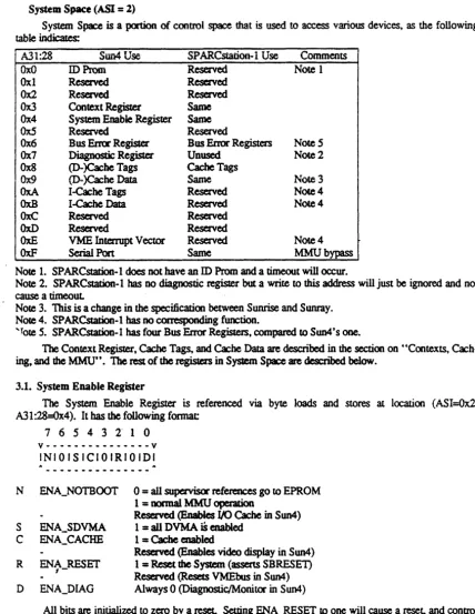
System Space (ASI
=
2)System Space is a p<xtion of control space that is use.d to access various devices. as the following
table indicates:
, A3 28
I A 1: .;)ur
use
SPAR'" t:stanOO-l use \...ommentsOXO IDProm Reserved
Note 1
Oxl
Reserved Reserved0x2 Reserved Reserved
0x3 Context Register Same
Ox4 System Enable Register Same
0xS Reserved Reserved
Ox6 BusEmrRe~ Bus Error Registers
NoteS
Ox7
Diagnostic Register UnusedNote
2Ox8
(D-)Cache Tags Cache Tags0x9 (D..)Cache Data Same Note 3
0xA I-Cache Tags Reserved
Note
40xB I-Cache Data Reserved Note 4
0xC Reserved Reserved
0xD Reserved Reserved
0xE VME IntemJpt Vector Reserved
Note
40xF Serial Port Same MMUbypass
Note 1. SPARCstation-1 does not have an ID Prom and a timeout will occur.
Note 2. SP ARCstation-l has no diagnostic register but a write to this address will just be ignored and not
cause a timeout.
Note 3. This is a change in the specification between Sunrise and Sunray.
Note 4. SPARCstation-l has no corresponding function.
"Tote 5. SP ARCstation-l has four Bus Error Registers. compared to Sun4' s ODe.
The Context Register. Cache Tags, and Cache Data are described in the section on "Contexts.
Cach-ing, and the MMU'·. The rest of the registers in System Space are described below.
3.1. System Enable RegSer
The System Enable Register is referenced via byte loads and stores at location (ASI=0x2,
A31:28=Ox4). It has the following fonnat:
7 6
5
4 3 2· 1 0v---v
INIOISICIOIRIOIDI
N ENA_NOTBOOT
o
=
all supervis« references go to EPROM1
=
normal MMU operationReserved (EnabIea I/O Cache in Sun4)
S ENA_SDVMA 1 = all DVMA
is
enabledC ENA_CACHE 1 = Cache enabled
Reserved (Enables video display in Sun4)
R ENA RESET t - 1 = Reset the System (asserts SBRESE1)
Reserved (Resets VMEbus in Sun4)
-0 ENA_DIAG Always 0 (DiagnosticIMonitor in Sun4)
All bits are initialized to zero by a reset. Setting ENA_RESET to one will cause a reset, and conttol
will not be returned to the program that does so; rather. a reboot will occur. Software (or the boot PROM)
should set ENA_NOTBOOT to one after initializing the MMU.
1.2. Bus Error RegisteiS
There are (our registers. divided into two sets of two, used to indicate the type and location of bus
ose that occur due to the execution of the current instruction and are reported to the CPU by a trap at the
end of that instruction's execution. All enors that cannot be associated with the execution of the current
instructioo. but are related to such things as DVMA activity, buffered writes. or cache write-back1, are
con-sidered asynchronous and are reported via an intmupt on level IS. After servicing the level IS interrupt. it
is cleared by toggling bit 0 of the Interrupt Register.
There is an exception to the above rule. On machines prior to the PI. 7 level, parity emrs that occur
(or any condition that causes SE_MEMERR. described below, to be set) during CPU memory accesses
cause the reporting of both a synchronous aDd asynchronous error. For parity errors that occur during data
fetches. the dala-access trap occurs first and the level IS interrupt remains pending. Software may clear the
level IS interrupt while processing the data-access trap. For parity ezrors that occur during instruction
fetches, the level IS interrupt occms first aDd the text-access trap IleVC'Z
occurs.
Software can distinguishttue asyncbronous errors from insttuctioo fetch errors by maintaining an
invalid
value in the SEV AR andcexnparing the SEV AR to the ASEV AR on asynchronous errors. If they canpare equal. then this is an instruction-fetch enor, otherwise it is a bUe asynchronous enor. Software must remember to reload the
SEV AR with the invalid value after processing all synchronous (including instruction-fetch) errors. On Pl.7 and later boards, memory errors during CPU memory accesses only cause the reporting of a
synchronous enor; a level 15 interrupt does not occur. (The asynchronous registers still latch on
synchr0-nous memory
errors.
however, and must be cleared; see the descriptions of the ASER and ASEV AR.~J
-The Bus Error Registers are all fullword in size. although they can be accessed via byte. halfwad, or
fullword loads and stores, just as memcxy is. They reside at the following ~ in ASI=2 space:
Address Desai om
Ox60000000 Synchronous Error Register
0x60000004 Synchronous Error Virtual Address Register
Ox60000008 Asynchronous Error Register
1x6OOOOOOC hronous Error Virtual Address R °
Although in nmnal use the regisfas can be treated as read-only, they can be written for diagnostic
pmposes.
3.2.1. Synchronous Error Register
The Synchronous Enu Register (SER) occupies four bytes at locatioos (ASI=0x2, A31:28=Ox6, A3:0=0x0 to Ox3). Reading any portion of the register also clears that portion. It has the following format
R
I
P T
B
M S W
31
23
IS7 6 5 4 3 2 1 0
v---v---v---v---v
10000000 0 0 0 0 0 000 OIRIO 0 0 0 0 OOIIIPITIBIMIOISIWI
...
..
..
---SE_WRITE SE_lNVALID SE_PROTERR SE_TIMEOUT
SE_SBERR
SF.,.MEMERR SE_SlZERR SE_ WATCHDOG
1
=
Error dming write cycle, 0=
read cycle1
=
Validbit.
zero in a page map entry1
=
Profedioa error (see below)1
=
Noo-existeIIt device ~ addressed1 = bus error during Sbus master access
1 = Memcxy (paity or ECC) error
1 = Incorrect size ttansfer attempted
1 = Restart due to
ru
errorThe
SER
records all errors since it was last cleared. Th~ includes asynchronous errors as well;the SER must be read to clear it as part of asynchronous error processing. The SE_ WRITE bit
Sun Confidential SPARCstation-l Programmer's Model DRAFI'
A protection error can be caused by an atte."npted "'rite to a read-()ldy page~ Of by a user-mode access
to a supervisor-only page.
A timeout is reported on access to a non-existent device~ except for accesses to non-existent physical
memory, See the section "'Type 0 Space/' below.
The Memory Error Register must be inspected when a memory error occurs~ to further isolate the
cause of the enot'. Note that synchronous memory errors also cause the Asynchronous Error Register and
Asynchronous Error Virtual Address Register to be latched; see the description of these registers below for
more infoonation.
Not all bus errors cause immediate tI3pS. Due to pipelining. the CPU fetches instructions four cycles
before they will be execu~ so it is possible that the CPU will attempt to fetch an instruction that will no~
in fact. be executed.. To prevent spurious trapS. the CPU does not trap on memory exceptions until it
actu-ally needs to execute the instruction that it was Wtable to fetch.
For example. suppose we have the following instruction sequence in virtual memory, where a., b, C,
etc. represent miscellaneous instructions:
a
b
bz~
d
label
page boundary
e <-this page is marked invalid
f
g
label:
x
y
z
page boundary <-this page is valid
These instructions will advance through the pipeline as follows:
1rune 1 2 3 4 5
Fetch d x y z
Decode bz d x y
Execute b bz d x
Write" a b bz d
At time (2), the (J>U wants to fetch e but the page is marked inval~ so the invalid bit is set in the SER and
the instruction address is set in the SEV AR. However~ the branch (if taken) means that e is never needed,
so that it would be incorrect for the CPU to U3p OIl a page fault due to the attempt to fetch e.
Now let's examine the following sequence: a
b
st something to a read-ooly page
d
page boundary
e ~ <--this page is nwked invalid f
g
The pipeline now looks as follows:
Time 1 2 3 4 5
Fetch d x y
Decode s1 d x
-~ecu1e b S1 d
.Ie attempt to fetch e from an invalid page at time (2) will turn on the SE_INV ALlD bit in the SER~ but
the CPU will not rake an instruction access exception until it actually needs to execute e~ at time (5). The
store to a read~y page at time (3), however, does result in an immediate data access exception, and the
CPU
win
find both the SE_INV AIlD bit and the SE_PROTERR bit on in the SER. (The exception resultsin a flush of the pipe, and instruction d never does get to the Write Slage in step (4».
A similar scenario, where the stole is replaced by a braDch (m user mode) to a supervisor-only page,
can result in multiple bits being 011 for insttuction access exceptions.
It is up to the software to determine the true cause of the exception when multiple bits are on in the
SER. Here is ODe aIgoridun:
SEV AR
=
gersevarQ;SER
=
SERsave=
getser();SER &= "(SE_ WRITE I SE_ WATCHDOG);
if (data access exception)
erroI'_addr = SEV AR;
else if (instruction access exception)
erIU_addr = old PC;
else
1* CAN'T HAPPEN
*';
if (SER & (SER - 1» (
1*
1* multiple bits 011; must manually probe the PME
*'
pme
=
getpme(eII'OI'_addr);if (pme valid) (
if «SER " SE_PROTERR) && (pine denies access» (
SER
=
SE_PROTERR;} else
SER &= "(SE_PROTERRISE_INV AUD); } else
SER = SE_INV
ALID:
*
Note: we could still have other multiple bits on(fIMEour,
*
MEMERR.
SIZERR. SBERR), but we probably won't recover from*
this condition anyway, so it really doesn't matter.*
*
But if you really wanted to, know you'd do something like*
this:*'
1* more than one of 11MEotrr, SBERR, MEMERR, or SIZERR
*'
(void) getser(); 1* make SUR iis clear
*'
if (on_fauk()
newSER
=-
getser();else (
, register int x;
newSER.=O;
x = *error_addr'; 1* probe the address to see what happens *'
}
no_fault();
Sun Confidential SPARCstatioa-l Programmer's Model DRAFr
2.2. Synchronous Error VD"tuaI Address Register
The Synchronous Error Virtual Address Register (SEV AR) occ!.tpies four byteS at locations
(ASI=0x2, A31 :28=Ox6, A3:O=Ox4 to Ox7). It contains the virtual address associated with the last
synchr0-nous bus error. It is DOt latched.
Note that on errors resulting from cache..fiU operations, the SEV AR will contain the address
that the CPU presented to the cache chip that triggered the cache-fill operation. This mayor may
not be the address or the word that actually caused the error.
The SEV AR has the following format:
31 0
v---v---v---v---'7v
I Virtual Address (A31:0) IA A
--- --- ---
---3.2.3. Asynchronous Error Register
The Asynchronous Error Register (ASER) occupies four byteS at locations (ASI=Ox2, A31:28=Ox6, A3:O=Ox8 to 0xB). Reading any portion of the register also clears that portion. It has the following fannat
31 23 15 7 5 4 0
v---v---v---v---v
I undefined IWIO ITIDI 0 0 0 0 I
A A
---
---
---
---W ASE_ WBACKERR T ASE_ TIMEOl.IT
D ASE_D~
1
=
Valid bit was zero in a page map entry1
=
Non-existent device was addressed1
=
busemr
during DVMAaccess
The ASER latches (freezes) with the cause of an asynchronous error, ignaing subsequent
asynchro-nous enot'S, until read and cleared. It is also latched wheJI a syaclarollous memory error
(SE_MEMERR) occurs, and shoald be read to unlatch it as part 01 SE_ MEMERR processing. Note
that bits in the SER are set when bits in the ASER are set; thus the SER sbould be read to clear it as
part or asynchronous error processing.
A write-back error can occur on systems with write-back cac~ and/or on systems that do buffered
writes~ when either the hardware malfimctioos or the MMU mapping is changed without properly flushing
the cache. In addition, certain devices (for example~ frame buffers) will generate write-back errors under device-specific conditions when a store is attempted to them.
A timeout is reported on access to a non-existent de~ except that accesses to non-existent
physi-cal memay may produce detectable bebavior otbez than timeouts. (See the section uType 0 Space,"
below.) For SPARCstation-l, this can only happen if the MMU is set up to map a non-existent device or if the hardware malfunctions.
The specific cause of a DMV A bus enu must be detennined by polling the possible sources to see
which indicated the emX'. AD possible sow'ces of DVMA errors of this type must be recognizable in some way. For SPARCstation-l. the only possible source of DVMA bus errors is memory parity errors. These can be detennined by examining the Memory Emr Register, described below.
D. to a bug in the cache chip, the ASER is Dot always set ",hell an asynchronous error occurs.
In tb~ event, tbe ASER am be reconstructed from the bits in the SER. SE MEMERR should be on
in the SER. In addition, SE TIMEOlIT indicates that ASE TIMEOlIT shOUld have been reported,
and SE SBERR indicates
that
ASE WBACKERR should have been reported. The address in theASEVER is correct even when the ASER is not set. This bug is in all versions 01 the hardware,
including P1.7's, and ~ not expected to be fixed.
3.2.4. Asynchronous Error Virtual Address Register
The Asynchronous Error Virtual Address Register (ASEV AR) occupies four bytes at locations ,ASI=Ox2, A31:28=Ox6. A3:0=0xC to OxF). It contains the (pseudo) vinual address associated with the
lChed. It is unlatcbed when it is read. not when the ASER is read. Thus, the ASEV AR should be read to
unlatch it as part of SE_MEMERR processing.
The ASEV AR has the foUowing formac
31 29 0
v---v---v---v---v IS SI
..
Pseudo Virtual Address (A29:0) I---.---
--
..
---
---S Bits 31:30
are
copies of bit 29.The address is called a upseudo-virtual" address because the hardware only carries the low-order 30 bits of the virtual address
onto
the bus, andassumes
that bits 31:29are
all thesa.me.
The ASEVAR revmesthis
process
by copying bit 29 into bits 31 and 30on
asynchronouserrors
reported by the IU. Due to a bug in the cadle chip, bits 31 and 30 are zero on DBMA asynchronous errors (ASE _ DVMAERR is on). Software must do the·sign extension itself.Determining the context register value associated with an asynchronous error is usually straightfor-ward; there is only
one
trickycase.
Since DVMA is always done using context 0, the address associated with a DVMA enor will always
be cmtext O.
Non-DVMA async:bronous tn'OI'S are due to buffer chip activity. The buffer chip allows only one outsranding SUR; a subsequent store will stall the CPU in the middle of execution of the second store until the outsanding store completes. If it completes with an asynchronous enor. the euor wiD be reported to the
CPU immediaIely after execution of the second store instruction finishes. (This is not necessarily
comple-tion of the second SUR itself. as it may itself be buffered. This is just completion of the store instruction
from the CPlrs point of view.) Unless the second store is a write to the context regisIer. the address of the
async:bronous
error
will beassocialed
with the value in the context regisIer (tile cunent context).If the second stQIe does modify the context regisIer. then the address of the asynchronous error is
associated with the previous ccaext. which must be determined by software. (If, for exampl~ the first
stole was to a supervisor-ooly ~ then the actual context is irrelevant as supervis«-on1y pages are
mapped into all CODtex1S.)
One can construct pathological cases where it would be impossible to determine that an
asynchro-nous enu is associated with the previous context (for example, a store to a user page, followed by a
branch, with the store to the context register in the delay slot of the branch). It is up to software to avoid
these pathologies.
3.2.5. Simultaneous errors
It is possible for both a synchronous and an asynchronous error to be reported simultaneously.
Con-sider the following
case:
st st
"&0.
[.,IO]! this address causes an asynchronous timeout"&0.
[.,Il]! this address causes a page faultDepending upon the alignment of the iDsttuctioos in the cache, it is possible for the IU to take the page fault trap (a syncbronous error) first. and while it is disabled for trapS but befcxe the SER has been read. the asynchronous fault can be reported. This will tum on the MEMERR bit in the SER, which can lead software to believe that this is a syDChronous memory errtt. Since the MEMERR is really asynchronous,
there will be a level 15 inttmlpt pendiDg. If software treats this error as synchronous, and diligendy reads
the SER. SEV
AR.
ASER, and ASEV AR to clear and/a unlatch them, then when trapS are evenwally enabled and the level IS intemtpt occurs software will discover tbat there is no infonnation in either theASER or the SER pertaining to the asynchronous interrupt.
SUD Confidential SPARCstation-l Programmer's Model DRAYI'
,no~ for it will recur if and when execution of the program is resumed.
3.2.6. Serial Port
The serial port is referenced by byte loads and stores at locations begi_n_n.i1'!g at (ASI::(.,~
A::OxRXJOOOOO). This access is provided so that the serial pM may be used before the MMU has been
ini-tialize<L for example by the PROM monitor. Software nonnally accesses the serial pat via I/O space
through the MMU.
See the section "Serial Ports" under "Type 1 Space". below. f(X'more information on the serial
port registers.
4. Pbysical Space
The MMU maps virtual addresses in Device Space to physical addresses in Pbysical Space. Physical
space is funher subdivided into four types. as indicated in the following table. Type Sun4 Use SP ARCstation-l Use Comments
0 MainMem<xy Same 1 I/O Space Same
2 VMEbus, 16-bit data Unused Note 1 3 VMEbus. 32-bit data Unused Note 1
Note 1. In SPARCstation-l, references to type 2 CI' 3 space cause a timeout
The size of
a
physical address is 28 bits.4.1. Type 0 Space
Type 0 space contains the main memory (RAM) in SPARCstation-l. Since PA27:O are used for
~ device decoding. the Sbus can support a theoretical maximum of 2S6 Mbytes of RAM. However,
e SP ARCstation-1 implementation only supports a maximum of 64 MbyteS. In addition, individual
~P ARCstation-1 machines can be configured with as little as 4 Mbytes of memory. To explain what
hap-pens when non-existent RAM is addressed. the implementation must be explained and some terms defined. .
The SP ARCstation-1 mem<X'Y subsystem contains two RAM controllers. Each RAM controller con-trols a "bank" of 32 Mbytes of address space. Each bank is made up of two "sets" spanning 16 MbyteS
each. Each set contains four SIMMs (Single Inline Memory Modules) each. Each SIMM consists of 9
chips. Each chip is either a 1 Mbit or a 4 Mbit DRAM. All the chips in a SIMM are of the same type. and
all the SIMMs in a set must be of the same type. A set of 1 Mbit DRAMs contains 4 Mbytes of memory, and a set of 4 Mbit DRAMs contains 16 MbyteS of memory. The SIMMs in one set can be of a different
type than the SIMMs in another set, even in the same bank.
The RAM controllers require PA27 to be zero. If PA27=I, then no controller responds and a bus timeout occurs.
PA26:25 selects the appropriate RAM controller. One controller responds to OxO. the other responds to Ox!. If PA26:25=2 (X' 3, eben no controller
.
responds and a bus timeout occurs .P A24 selects one of the two sets of SIMMs controlled by a controller. If the selected set is not installed (a bole), then OIl writes the data is thrown away and on reads the bus lines remain high (subject to
noise) and a characteristic bit pattern (normally all ones) is returned. Software can detect a hole by doing a
store to fpllowed by a load from a byte on 16 Mbyte boundary. If the data read does not agree with the
data wriue~ then a hole exists. If they agree, the saIne test \\-;th a different bit pattern should be used
before concluding that real memory exists. (Note that parity checking should be disabled when doing these
checks, as parity errors will be reported if the noise pattern conrains bad parity and parity checking is enabled.)
If the selected set consists of 4 Mbit DRAMs, then all 16 Mbytes of address space spanned by that
set are valid and correspond to unique memory locations. If the selected set consists of 1 Mbit DRAMs. then only 4 Mbytes of unique memory exist. but it 3ppe3-rs four times in the 16 ~1bytes of address space anned by the set, repeating at every 4 Mbyte boundary. This "mirror" behavior can be detected by .Alftware by doing a store of one bit pattern to offset 0 of a SC4 followed by a store of another bit pattern to
I the stOre to offset 4 Meg, then only 4 Mbytes of memory is present and the rest is filled with mirrors.
The following decision table swnmarizcs this bebaviO'.
PA27 PA26 SIMMSet PA23:22 Action
1
-
-
-
Tuneout0 1
-
-
Tuneout0 0 none
-
Hole0 0 4Mbit
-
Memory (16 Mbyres w<X1h) 0 0 1 Mbit 00 Memory (4 Mbytes worth)01
0 0 1 Mbit 10 Mirror 11
4.2. Type 1 Space
Type 1 space contains all of the JJO devi~ including those that are associated with the Sbus. Bit PA27 is used to indicate an onboard device (PAZl=O) or an Sbus device (pA27=1). For OIlboard devices, PA26:24 (and in some cases PA26:20) determine the particular device. For Sbus devices, PA26:2S select one of four Sbus slots. The (physical (X' logical) board plugged into the Sbus slQt then bas an address space of 2S bits, or 32 Mbytes, to divide up as it sees fit. Sbus 3ddressing is furthel' described in the Section
"Sbus Devices" t below. For compatibility with the Sun4 architecture conventioos, the non-existent bits
(PA31:28) are assumed to be aD ones. The following table descn1>es the layout of Type 1 space:
Address SPARCstation-l Use Comments
0xF(X)()()()()( KeyboardlMouse Note 1
OxFlOOOOOO Serial Ports Note 1
0xF2000000 TOD Clock and NVRAM Note 2
JxF3000000 Countt.r-TUDa' Registm Note 3
0xF4000000 Memory Enor Registers Note 1
OxFSOOOOOO IntemJpt Regisler Note 1
0xF6000000 EPROM Note 3 0xF7000000 EPD "Private": Note 4 0xF7100000 ECC registers (HPDonly)
0xF7200000 Floppy Controller 0xF720 1 ()()() AudiollSDN
0xF7400003 Auxiliary Input,()utput Register
OxF7FOOOOO VME Control Register (SunFed only)
0xF8000000 Sbus Slot 0
as
bils) Note 4 0xF9000000 "..
OxFAOOOOOO Sbus Slot 1
as
bits) Note 4 0xFB000000..
..
0xFC000000 Sbus Slot 2
as
bils) Note 40xFD000000
..
I..
0xFE000000 Sbus Slot 3
as
bUs) Note 40xFR)(X)()()()
..
..
Note 1. $iame as Sun4 use.
Note 2 Sun4 has a different kind ofTOD at this address. It also has an EEPROM at a different address. Note 3. Sun4 has same f~ but at a different address.
Note 4. Sun4 has no corresponding function.
SUD CODfidential SP ARCstation·l Programmer's Model DRAFr
2.1.1. KeyboardIMouse
The keyboard/mouse UART is a Z8530 chip (Ziiog or AMD equivalent) accessed via byte loads and
storeS at the following addresses:
Address
0xF0000000 0xF0000002
0xF0000004
0xF0000006
Description
Mouse Control Port
Mouse Transmit (W)/Receive (R) Data Port
Keyboard Control Port
Keyboard Transmit (W)/Receive (R) Data Pat
The Z8530 contains an array of read registers and write ~ accessed through the control port.
Access to a register is done by writing the register index to the control p<X4 and then reading or writing the
register data to the control port. In addition. the UART ttanSIllit and receive data registers may be directly
accessed by writing and reading. respectively. from the TransmitIReceive Data Port.
See the Z8530 data sheet for more information.
4.2.1.2. Serial Ports
The serial portS UART is also a Z8530 chip. identical to the one used for the keyboard/mouse. It is
addressed as follows: Address
OxFlOOOOOO 0xF1000002 0xF1000004 0xF1000006
I
Serial Port B Control Port
Serial Port B Transmit (W)/Receive (R) Data Pat
Serial Port A Control PM
Serial Port A Transmit (W)/Receive (R) Data Port
2.1.3. TOD Clock aDd NVRAM (EEPROM)
The Tune of Day Clock is a Mostdc MK48T12-15 Zeropowca.r/f"lDlekeeper RAM which includes 2K
of RAM, the topmOSt 8 byteS of which are the clock. The Tunekeeper contains its own battery backup,
which has a worst-case storage life (oscillator off or powec on) of II years at 700C and a worst case
con-sumption life (oscillator on and power off) of 2.8 years at OOC. Unlike EEPROMs, there is no limitation on
the number of times the CMOS RAM can be written, nor are special write timings required.
The CIoclclNVRAM is accessed via byte, halfword, or fullword loads and stores at the following addresses:
Address
0xF2000000 to
OxF2OOO7d7
0xF20007d8 to
0xF20007f1 0xF20007f8 OxF2OOO7f9 OxF2OOO7fa OxF2OOO7fb. 0xF20007fc OxF?J.XXt1fd 0xF20007fe OxF2OOO7ff
"IDPROM"
TODCootrol
Seconds (00-59) Minutes (00-59) Hour (00-23) Day (OI..Q7)
Date (01-31)
Month (01-12) Year (00-99)
Thirty-two bytes of NVRAM acts as the ID prom" of SPARCstation-l. The id_machine byte con-tains Ox51; Ox50 is the architecture code for Sun4C, and Ox51 indicates the SPARCstation-l machine.
The TOO Control register should only be written with byte stores to prevent modifying tbe data to be read.
The time and date information is stored in 24 hour BCD format For more infonnation, including the
2.1.4. Counter-Timer Reamers
The Counter-TImer Registers are accessed via fullword loads and stores at the following addresses:
Address
0xF3000000
0xF3000004 0xF3000008
0xF300000C
Counter 0
Limit 0 Counter 1 Limit 1
All registers have the foUowing format
31
9o
v--~---v---v---v---v
ILl 21-bit value 10 0 0 0 0 0 0 0 0 01.
L Limit Reached
Each counter is inaemented by one in bit position 10 at one microsecond intervals. When a counter
reaches the value in its corresponding limit register. it is reset to "one ~'t the limit-reached bit in both the counter and limit registers is set. and an intemJpt is generated .(if enabled) at level 10 for
COlDlter 0 and 1eve114 f<r Counter 1.
The intemJpt is cleared and the limit bilS reset by reading the appioprWe limit register. Reading the
counter register does not change the scare of the limit bits. Writing the limit register resets the counter
register to a value equivalent to one microsecond. Except for testing purposes. the counter registers should
not be written.
Setting a limit register to zero causes the corresponding counter to freerun. IntenUptS will occur
-'rben the counter overiIows back to zero. approximalely every 2 seconds.
4.2.1.5. Memory Error Rewisters
SP ARCsta1ion-1
uses a
single Parity Control Register. This isa
fullword read/write register atloca-tion 0xF4000000 in Type 1 physical space. The format of this register is as follows:
31
23
15
7
0
v---v---v---v---v
10 0 0 0 0 0 0 0 0 0 0 0 0 0 0 0 0 0 0 0 0 0 0 OIEIMITINIAIBICIDI
6 6
---E Parity Emx'. Set on any parity error.
M Multiple Errors. Set when
a
parityenor occurs
and E= 1.T Parity TesL When set, inverse parity is generated.
N Parity Check. Enables parity cb«king.
A Parity Enu 24. Recards parity error on data bilS 31:24.
B Parity EmX' 16. Recards parity error 011 data bits 23:16.
C Parity E.nu 08. Recards parity error on data bits
15:8.
o
Parity E.nu 00. Records parity error on data bits 7:0.The bits that indicate errors
<a
M, and A-D) are cleared when the register is read. All bits are cleared onreset. '
Note that when
a
parityel1'Or occurs,
the cache willhave
loaded itself with the daIa frommemory
anyway. This means that software must flush the cache after parity errors if it is to continue operation. On
a single parity error (M=O). only the affected cache line (as detennined from the old PC. the SEV ARt or
Sun Confidential SPARCstation·l Programmer's Model DRAFr
2.1.6. Interrupt Register
The Interrupt Register is a one-byte read/write register at location <r~5000000 in Type 1 physical
space. The fonnat of this register is as followed:
7 n U
\1
S-;:;
~
~
v---v
IAIOICIDIEIFIGIHI
A Enable Level 14 Interrupts C Enable Level 10 Interrupts D Enable Level 8 Interrupts
E Software Interrupt Level 6
F Software Interrupt Level 4
o
( w
~~
I~:
ol:;.
~-V.) ~
l.)
(""'\-
~c).'C)
?)
G Software Interrupt Level 1
H Enable all Interrupts
Writing a zero to an Enable Level N Interrupt bit only masks out that interrupt. it does not clear the source. Writing a one to a software interrupt bit requests an interrupt on that level; the bit must be cleared to clear
the request.
Writing a zero to the Enable All Interrupts bit will clear the AsynchronolJs Memory (level 15)
Inter-rupt, as well as masking all interrupts. Of course, interrupts should be immediately re-enabled by writing a
one.
On reset, all bits are cleared and all interrupts are reset.
4.2.1.7. EPROM
SP ARCstation-l has 128K byteS of EPROM containing the boot monitor beginning at location
:F6OOOOOO in Type 1 physical ~ Tbe EPROM is also referenced by all Supervisor Vinual addresses .vhen the ENA_NOTBOOT bit in the System Enable Register is zero, for example at boot time. The boot
code must initialize the MMU to at 1east map itself befcxe setting the ENA_NOTBOOT bit to one.
Note that the EPROM does not obey the nonnal memory mapping rules. PA[16:0] into the EPROM always come from VA[16:0]. Although VA[29:12] are processed by the MMU to select a physical address, when bits PA[27:24] of that physical address select the EPROM then bits PA[23:12] from the
MMU are ignored. This means
that.
for proper operation of the EPROM, it must be mapped one-for-one tocontiguous virtual pages beginning on a 128K boundary. 4.2.1.8. Floppy Controller
The Floppy Disk Conttoller is an Intel 82072. It is accessed using byte loads and stores at the fol-lowing addresses:
IA~
0xF7200000 Main Slalus (R)JDala~
Rare~
Register (W)I
. 0xF7200001 FIR) Data Port (R/W) , .
For more information see the Intel 82072 daIa sheet Note that the floppy must be selected as drive 1 (or 3, but 1 is preferred) in the command sequence sent to the conttoller. See also the Tenninal Count and Aoppy 1!ject bits in the -Auxiliary Input/OulpUt Register-descnDed below.
4.2.1.9. AudiollSDN
The audio interface of the SP ARCstatiOll-l is provided through the Main Audio Processor (MAP) of
the AMD 79C30A Digital Subscriber Controller. The 79C30A is a highly integyated circuit which pro-vides an ISDN 4-wire subscriber level interface, an audio processing circui~ a parallel microprocessor interface, and a serial interface. For SP ARCswion-l Audio use L~ microprocessor interface 2.'ld the audio
The interrupt from the 79C3O is attached to IRQ< 13> of the MMU (which is interrupt level 13). The
data bus is conoected to the 10 data bus. The circuit includes an oscillator circuit which uses an externally
provided 12.288 MHz crystal with a tolerance of + or -80 ppm. The oscillator is a pam1le1 resonant circuit
The 79C3O registers are located at a base address of 0xF7201000. The 79C3O is accessed using byte
loads and stores at the following addresses:
Address WR* RD* Register
on
0xF7201000 0 1 Ccxnmand Register (CR), write only
1 0 Interrupt Register (IR), read only
0xF720 100 1 0 1 Data Register (DR), write
1 0 Data Regisla' (DR), read
0xF7201002 1 0 D-channe1 Status Register 1 (DSR1). read only
0xF7201003 1 0 D-dwmel Error Register (DER). read only
0xF7201004 0 1 D-channel Transmit Buffer (DCTB). write only (8-byte FIFO)
0xF7201004 1 0 D-channel ReceiVe Buffer (DCRB). read only (8-byte FIFO)
0xF720100S 0 1 Bb channel Transmit Buffer (BBTB). write only
0xF720100S 1 0 Bb channel Receive Buffer (BBRB). read only
0xF7201006 0 1 Be channel Transmit Duffel' (BBTB), write only
0xF7201006 1 0 Be channel Receive Duffel' (BBRB), read only
0xF7201007 1 0 D-channe1 SIabJs Register 2 (DSR2), read odly
Note that the other registers in the 79C30, of which there are many, are indirectly accessed through
the cc:mmand register. Pages 2-71 through 2·77 of the 79C3OA Data Sheet describe this iDdirect address·
ing.
Please refel' to the 79C30A Data Sheet for full details on operation of this circuit
".2.1.10. Auxiliary Input/Output Register
The Auxiliary Input!Output Register is a one-byte, read-write register at locaIion 0xF7400003 in
Type 1 physical space. It has the following format:
7 6 5 4 3 2 1 0
v-.--- •••• - ••••• v
11 IIDICISITIEILI
o
In DensityC In Floppy Diskette Change (must be written
as one)
S Out Floppy Drive Select
T Out TC (Floppy controller Terminal Count input)
E Out Floppy Eject
L Out LED (l=<Xl, O=off)
All bits are set to one on reset.
Bit 5.(Density) is a signal from the drive indicating the density of the diskette inserted. A 1 indica1es
high density, a 0 indicares low density. This signal is meaningful only if the floppy drive is capable of
sensing the "density" hole in the diskette. The Sony drives do not generate this signal; for them, software
must through trial and enor determine the density of the imerIed diskeue This can be done by initializing
the conb'Oller with paramettzs for a given density and attempting to read the diskette; if the wrong
parame-ters were chosen read errors will occur. Note that the density of an unformatted floppy cannot be
deter-mined through this method; the floppy format software must have a user option to set the density to be
used. (If the user selects the wrong density, the floppy will be Wlusable, but the user will quickly discover
Sun Confidential SPARCstation-l Programmer's Model DRAFr
.!Set signal: a bit wHi need to be provided foc this function in the Auxiliary Input/Output Register if a
non-Sooy drive is chosen for SPARCstation. When will th~ dKision be made?
Bit 3 (Floppy Drive Select) is connected to the fJappy drive select pin. It is used in conjunction with
all Boppy \'"e.."3tior~ whether t&'1rough tbe Flvypy Disk Controller registers or the bits in the Auxiliary i/O
Register. A one selects the fJoppy drive; a zero deQselects it.
Bit 2,(TC) is connected to the Taminal Count input pin of the fJappy controller. It is used to signal
the fJappy controller (which is designed to be connected to a DMA controller, even though in
SPARCstation-l it is not) that all the data for a given operation has been transferred. This is done by
writ-ing a 1 to this bit. delaying for a specific amount of time, and then writing a 0 to it. (The specific amount of
time depends upon the data rate and can be found in the Intei 82072 data sheet.)
Bit 1 (Floppy Eject) is connected to the fJappy drive eject mechanism. To eject a fJappy, set bit 3
(Floppy Drive Select), wait 20 m~ set bit I, hold it set for at least 2.0 microseconds, then reset
both it and bit 3 to zero.
Bit 0 (LED) controls the LED on the front ~1.
Unused bit positions should be written with ones when writing to the register. This will allow them
to be used fa' input signals if this becomes necessary.
4.u. Sbus Devices
Unlike previous busses. the Sbus is geographically addressed. PA26:25 select which of four Sbus
"slots" is being referenced. A board plugged into an Sbus slot has PA24:0, a' 25 bits or 32 MbyteS of
address space addressability to divide up among the devices contained 00 that board. A Forth program
beginning at offset 0 of the slot descnOes the devices on that board to the system. The details of the Forth
specification are described in Sun Forth User's Guide.
Slot 0 is not a physical slot. Rather, it refers to the onboard D~ SCSI, and Ethernet controllers
lich~ for convenience~ are viewed as being plugged into Slot O.
Slots 1, ~ and 3 are physical sloes inlo which the user may plug boaIds containing devices. Slots 1
and 2 have DVMA-masta' capability; slot 3 is a siave-only slot and does not supp<Xt boards that operate as
DVMA masters. The board containing the video subsystem (video control registers~ RAMDAC~ and frame
buffer) is usually, but need not be, plugged into Slot 3.
If no device responds to a particular Sbus address. a bus timeout will occur.
The following table summarizes the devices:
P A26:25 Device
00 Onboard DMA. SCSI, and Ethernet controllels
o
1 Sbus Slot 11 0 Sbus Slot 2
1 1 Sbus Slot 3 (usually video subsystem)
.
4.u.l. DMA, SCSI, aDd Ethenaet Devices
The following table describes the offsets to the ooboard D~ SCSL and Ethernet devices~ relative
to the beginning of Sbus "Slot 0" ~ physical address 0xF8000000 in Type 1 space).
Offset
OXOOOOOO
Ox400000 Ox800000
OxCOOOOO
Description
ID (4 bytes~ OxFESlOlOl)
DMA Registers
SCSI Registers
Ethernet Registers
4.2.2.1.1. DMA Registers
The DMA registers are accessed via fullword loads and stores to the following offsetS (the addresses
Address
Ox400000 Ox400004 Ox400008 Ox4OOOOC
, 'OIl
DMA Control/Status Register
DMA Address Register
DMA Byte Count Dia tic Re .
The DMA registers are used when programming SCSI operations. Other than the ILACC bit in the
DMA ControVStatus Register, they are not used when programming Ethernet operations.
4.2.1.1.1.1. DMA CODtroIIStatus Register
The DMA ControVStatus Register has the following fonnat:
31 27 15 12 10 8 6 4 3 1 0
v---v---v---v---v
IDEV_ID ,. unused (read as ze ro) ILl TICIADRI P INIWIRIDI F I I I PCKIE I J I
A A
---
---
---
---.---DEV_ID
DEV _ID. Device ID. Read-only. (ObIOOO in this implementation.)
L L. ILACC. When 0, the EthemetIDMA intetface is configured to use the Lance Ethernet cClltroller.
When 1, the interlace is configured to use ILACC, "the new Ethernet chip from AMDpq (Cliff
Buckley).
T TC. Terminal Count. Read-only. Byte counter bas expired. This bit is cleared by setting the Flush
bit (bit 5).
C EN_orr. Enable Count. Rea<Vwrire. Enables tile DMA Byte Count Register. (Not used in normal SP ARCswioo-l operation.)
DR BYIE_ADDR. Read-only. Next byte number to be accessed
P REQ..PEND. Request pending. Read-only. Set when tile DMA interface is active. RESET and
FLUSH must not be assetted ifREQ..PEND is ODe.
N EN_DMA. Enable DMA. Rcad/write. Set to enable DMA activity. reset to disable.
W WRITE. Read/wrire. Set for DMA from device to memory (read), reset for DMA from memory to
device (write).
R RESET. Read/wrire. When set, acts
as a
hardware reset. ERR_PEND. PACK_CNT. INT_EN. FLUSH, DRAIN,WRI"IR
e'-D~ REQ...PE.ND. EN_CNT. and TCare
all set tozero.
RESETremains at 1. and must be set bact to 0 by software to reswne operation.
D DRAIN. Read/wrire. Set to force remaining pact register byteS to be drained to mema-y. Oears itself.
F FLUSH. Wrire-001y. Set to foce PACK_CNT and ERR_PEND to zero. Also clears TC and the
interrupt TC=1 causes. Always reads,as zero.
I !NT_EN. IntemJpt enable. Readlwrite. Set to enable intemJpfS.
PCK PACK_CNT. Pack Count. Read-only. Number <X bytes in Pack Register.
E ~_PEND. Error Pending. Read-only. Set when a memory exception occurs. Reset by seaing FLUSH. DMA activity stops until reset.
] INT_PEND. Interrupt Pending. Read-only. Set when TC=l or when external device
raises an
inter-rupt. Cleared when read (if TC=I is the cause) or by servicing the external device (if that is the
cause).
"
SUD Confidential SPARCstation-l Programmer's Model DRAFT
..,
.
-'I 23
o
v---~~~~ee====V=---v---v---v
IVA31:24-latchedl _ _ _ _ _ _ _ _ _ _ _ _ _ _ _ A _ _ _ _ _ _ _ _ _ _ _ _ _ _ • VA23:0 -~ e = = = - . _ _ _ _ _ _ _ _ _ _ _ _ _ _ _ _ _ _ _ _ _ _ _ _ _ address _
The high byte is latched by the hardware and indicates which 16 Mbyte region of Virtual Memory is
accessed. (The MMU recognizes a DMA virtual address and f<rees Context 0 to be seJected.) The
low-order 3 byteS contain the address of the byte to be transfetred. Rollover is only through the low-order 24
bits.
4.2.2.1.1.3. DMA Byte Count
The DMA Byte Count Register has the following fonnat:
31 23
o
v---v---v---v---v
10 0 0 0 0 0 0 01 BCNT23:0 - counter I
_ _ _ _ _ _ _ _ _ _ _ _ _ _ _ A _ _ _ _ _ _ ~ _ _ _ _ _ _ _ . . A _ _ _ _ _ _ _ _ _ _ _ _ _ _ _ A _ _ _ _ _ _ _ _ _ _ _ _ _ _ _
This register is only used when EN_CNT is 00 in the DMA ConttolJ'Status Register, and so is not
used in normal SP ARCstation-l operation. The bigh byte is Wlused and
wiJl
always read back as zero.The low <Xder bytes contain the number of bytes to be transferred. and counts down to zero. When zero is
~ TC, and thus INT_PEND, are set to
one.
Further DMA transfers cannot take place until a newvalue is loaded into the Byte Count Regiser.
4.2.2.1.1.4. Diagnostic: Register
The format of the Diagnostic Register is not available.
2.2.1.2. SCSI Registers
The SCSI registers are accessed via byte loads and stores to the following offsets (the addresses in
this table do not include the slot base address, which must be added to the device offset):
Address Description
Ox800000 Transfer Count Low
Ox8Q0004 Transfer Count High
Ox800008 FIFO Data
0x80000C Command
Ox800010 StatuslBus 10
Ox800014 InterruptlStatus Tuneout
Ox800018 Sequential step/Syncbroniza1ion transfer period
Ox8000 1 C FIFO ftags/Syncbronizatioo offset Ox800020 Configuraboo
Ox800024 Clock Conversion Factor (write only)
Ox800028 ESP "lEST (chip test use oriIy) Ox80002C ESP IT Configuration-2
Note that byte accesses must be performed even though the addresses are all fullword-aligned. :
Since the SCSi controller uses the DMA controller to perfonn the actual transfer of data to and from memory. the two devices must be programmed together. One possible algorithm is as follows:
scsi_stanO
{
1* stan an operation on the SCSI *1
lock: data pages into contiguous virtual memory;
DMA_address_registet
=
starting virtuai address;setup SCSI registers (except for "go");
DMA_cootroCstatus_register
=
(EN_DMA I !NT_EN I (other bits»;,. The SCSI will interrupt us when it is done.
*'
scsi_intemlptO
(
,. must drain DMA on a read from
disk/write
to memory*'
if (last operation = READ) {
For a detailed desaiption of the SCSI registers, see the NCR 53C90 Data Sheet
4.2.2.1.3. Ethernet Registers
The Ethernet registers are accessed via halfword loads and stores to the following offsets (the
addresses in this .table do not include the slot base ~ which must be added to the device offset):
I
0xC00000 Address RegisIer~
DaIa Port (RDP)I
. 0xC00002
Regis!er
Address Port (RAP) .For a detailed description of the Ethernet registers, see the AMD Am7990 Data Sheet
4.2.2.2. Video Subsystem
The following table describes the offsets to the devices located on the Video Subsystem Board.. This
board is usually plugged into Sbus "Slot 399
(base phySicaJ address OxFEOOOOOO in Type I space).
Offset
.JxOOOOOO 10 (4 bytes, OxFEOIOIOI) Ox400000 Video aDd DAC Registers
OxSOOOOO Frame Buffer
4.2.2.2.1. Video and DAC Registers
The Video and DAC registers are accessed via byte loads and stores to the following offsets (the
addresses in this fable do not include the slot base ~ which must be added to the device offset):
Address
Ox400000 Ox400001 Ox400002
Ox400003
Ox400004
Ox40000S
Ox400006
Ox400007
Ox400008
Ox400009
Ox40000A
Ox40000B Ox400010 Ox400014 Ox400018
Description Video Cootrol Register Video Status Register
HBS (Horizontal Blank Set)
HBC (Harizcotal Blank Clear)
HSS (Hcrizcxual Sync Set)
HSCO (HorizomaI Sync CldIr, !VS)
HSCI (Hcrizcxual Sync Clear, VS)
VBSH (Vatical Blank Set High Byte) VBSL (Vatic:al Blank Set Low Byte)
VBC (Vertical Blank Qtar)
VSS (Vertical Sync Start)
VSC (Vertical Sync Clear)
DAC Address Register
DAC Color Palette Register Port
Sun Confidential SPARCstation-l Programmer's Model DRAFT
Note that the DAC registers are 8=bits wide even though they are aligned on fullword boundaries. FuJlword accesses can be used to quickly read or write one or more palette entri~ by storing tbe index of
the first palette to be accessed in the address register and then doing full word accesses to the appropriate
palette port The data must be packed into bytes in the ooier • 'RGBRGBRGBRGB "; if! aliter words, 3 fullwords will hold 4 palette entries. Palette entries are only stored when the Blue value is written; partial update of a palette is not possible.
4.2.2.2.2. Frame Buffer
The fiame buffer is a megabyte of RAM occupying offsets from OXSOOOOO to Ox8FFFFF. Each byte
corresponds to one pixel Accesses may be by byteS. by halfwonb, or by fullwords.
If the frame buffer is only half-~ then only the lower four bits of each byte will be
significanL As the upper four bits will be (weakly) pulled up with resistors, only the upper 16 color map entries (entries 240 through 255) in the DAC will be usable. Software can detect this case by writing, then reading, the frame buffer. If the upper four bits always read back ~ ones, independent of the data written,
then the ~ buffer is half-pop~ (This 11 grody - Ed.)
5. Interrupt Levels
The following table describes the interrupt levels defined by the S.un4 Architecture and the
SP ARCstation-l implementation.
Level Sun4 Use SPARCstation-l Use 15 Memcry Error Asynchronous Memory Emx
14 Oock: Counter 1
13 VMEbus level 7 Audio 12 Keyboard, Mouse, Serial Pons Same 11 VMEbus level 6 Floppy
10 Oock Counter 0
9 VMEbus levelS SbusIRQ7
8 Video SbusIRQ6
7 VMEbusievel4 Video, Sbus IRQ5
6 Ethernet, Software request 6 Software request 6
5 VMEbusieve13 Ethernet. Sbus IRQ4
4 SCSI, Software request 4 Software request 4
3 VMEbusievel2 SCSI, DMA, Sbus IRQ3 2 VMEbus level 1 SbusIRQ2
1 Software request 1 Same, plus Sbus IRQl
6. Resets
Although there is only
one
type of reset in SP ARCstation-J (a reset of the entire machine that causes system registers to be restored to a known state), thete are three ways to effect a reset:(1) Power-on. A power-on reset (POR)
oCcurs
when power is initially applied to SPARCstation-l. (2) Watchdog. A watchdog reset occurs when the IU signals an error condition. This can occur, forexample, if the IU attempts to take a trap when traps are disabled.
(3) Software. Software can initiate a reset by writing a one to the ENA_RESET bit of the Sysr.em Enable Register.
The SE_ WATCHDOG bit in the Synchronous Error Register is set to one on watchdog-initiated
resets, and set to zero for all other resets.
7. Contexts, Caching, and the MMU
This section describes the interaction of the context register, the cache, and the MMlJ from the
1. Context Repler (ASI=2, A=0x30000000, byte access only) The Context Register has the following format
7 3 0
v---v
10 0 0 01
CID1
Note that although the
em
isfour
bits wide, only the low-order 3 bits (CID2:0)are
actually used. CID3 isignored.
The context register selects one of 8 contexts for translating User Mode
addresses.
It exists in both the Cache and the MMU. ...rFi= _ _ _ _-Programming note: A byte store (STBA) into (ASI=2, A31:28=0x3) writes both the MMU and Cache Context Registers. A byte load (LDUBA, LDSBA) from (ASI=2, A31:28=0x3, AO=O) reads the
MMU's Context Register, and a byte load from (ASI=2, A31:28=0x3, AO=I) reads the Cache's Context Register. The ability to read each register separately is provided for diagnostic purposes; they should always contain the same value and standard software will usually just read the MMU's Context Register.
7.2. MMU decoding of Virtual Addresses
From the MMU's standpoint, a virtual address has the following formac
3 I 29 17 II
o
v---v---v---v---v
1 1 1 page in 1 I
1
1
segment (12 bits)1
segment Ibyte in page (12 bits)I
I 1
..
I (6..
bi ts) I..
I---
---.---
---)te: V A31:29 must aU be the same (aU 0 or all I). An SE_INV ALID em.-results otherwise.
CID2:0 is concalenatCd with V A29: 18 to select one of 32K segment map entries. (One can view the
segment map as consisting of 8 contexts, each context containing 4K segments.) The segment map entry is
8 bits wide, although only the lower 7 bits are used, and points to a Page Map Entty Group (PMEG): 7 6 0
v---v
101 PMEG I
PMEG6:O is concatenated with VA17:12 to select
one
of 8K Page Map Entries (PME). (Onecan
view the page map as consisting of 128 PMEGs. each PMEG containing 64 pages.) The PME is 32 bits wide. organized as follows:
31 29 27 25 23 15 0
v --- ---v .. --- --. - ----v ---v .. ---v
IVIWISIXITYPIAIMIO
0 0 0 0 0 0 01
physical page number (16 bits)1A A . . . . A
---._.---
---V l=entry is valid
W I,::write
access
allowedS l=Supervisor mode
access
onlyX 1 =don 't cache this page
TYP O=Main Memory; l=Sbus and IIO space; 2.3=reserved for VMEbus
(~-A l=page has been accessed
Sun Confidential SPARCstation-l Programmer's Model DRAFT
A page is 4K bytes. A segment is 64 pages or 256K bytes. A context contains 4K segments or IG
byte. This Jast is divided into two address ranges of 512M: bytes each~ from OxOOOOOOOO-Oxifffffff
and from OxeOOOOOOO-Oxffffffff.
(2) Unlike architectm~ used by other vendors. in this architecture there is no way to explicitly mark a
segment as invalid However. the opemting system can reserve one PMEG and mark all of its PMEs
invali<L and then point invalid segments at this PMEG. sunOS has traditionally used the last PMEG
for this purpose. but this may be subject to change.
":-:"'\ (3) ~ecause the ca:be ignores the
context
register when resolving accesses to supervisor-mode-only~ ~
the
temei
se~ ~be
.identical in each c~text This can be accomplished by repeaung the same PMEu m the app-opnatc segment map entnes.(4) A context is selected by performing a byte store into the Context Register (ASI=2. A31:28=0x3). A segment map is initialized by selecting a context. and then penorming byte stores into (ASI=3, A29:18=OxO to Oxfff). (Half and fullword stores will work but are not recommended.)
A PMEG is initialized by selecting
a
con~t. and then performing fullword stores into (ASI=4, A29: 18=desired segment. AI7: 12=OxO to Ox3f).(5) The hardware does not insure consistency between the cache and the MMU. The operating system software must Bush the cache appropriately before updating the
MMU.
Before changing the mapping of a context, a Flush Cache (Context) opercUion must be performed. Before changing the mapping of segment. a Flush Cache (Segment) operation must be peIformed. Before changing the mapping of a page, a Flush Cache (Page) operation must be performed. These operations are desaibed in the Cache section. below. Also note that these are not the only circumstances' when flushing the cache is necessary.7.3. Cache decoding
or
Virtual AddressesTo improve penormance. SPARCstation-1 contains a 64K byte
virtual
address cache, consisting of.A lines· of 16 bytes each. The cache is one-way set associative, with each virtual address mapping to one
and only one possible cache line. There is a 4 byte cache tag associated with each data line. From the Cache's standpoint. a virtual address has the following format
31 29 15 3
o
v---v---v---v---v
I I I Ibyte ofl
I I cache tag id (14 bits) I cache line (12 bits) I line I
I I I I (4 b.) I
A A A
---
------Note: V A31:29 must all be the same (alI 0 or alii). An SE_INV ALID error occurs otherwise.
V A15:4 selects one of 4K cache lines. If the cache tag id matches (and, for
non-supervisor-mode-only pages, the context ID), then a cache hit
occurs.
V A3:2 selects the desired word from the cache line.A cache tag has the following f~
~~-.O-O-O-O-O-O~~~iD-~~is\v~~-o-or:--~~~h~-~~~-idV(i4-bi~;;--i~-~~
,. I .. .. ..A
_ _ _ _ _ _ _ _ _ _ _ _ _ _ _ _ _ _ _ _ _ _ _ _ _ _ _ _ _ _ _ _ _ _ _ _ _ _ _ _ _ _ _ _ _ _ _ . . . _ 0 = = _ _ .. 5 ...
CIn Cache Tag Context (copied from Cache Context Register when cache line is filled.) Note that only CID2:0 are present
W l=write access allowed (copied from MMU when cache line is filled.) S l=Supervisor mode access only (copied from MMU when cache line is filled.)
V 1 =entry is valid
) 1be cache tagS must be initialized by software before the cache is enabled, by clearing the valid bit
in the cache tag of each cache line. It is sufficient to do fullword stores of zero into (AS 1=2, A31:28=Ox8. A15:4=OxO to Oxfff).
(2) To Bush all references to a COOleXt from the cache. a Flush Cache (Context) operation must be
performed by selecting the appropIiare context (by performing a byte store into the Context Register,
(ASI=2, A31 :28=0x3» and doing fullword stores of zero into (ASI=Oxe. A 15:4=OxO to Oxfft).
(3) To flush
an
references to a segment from the cache. a Flush Cache (Segment) operation must beperformed by selecting the appiopaiate conrext and doing fullward stores of zero into (ASI=Oxc, A29:18=desired segment. A15:A4=OxO to Oxfff). A17:16 are ignored for this operation.
(4) To Bush
an
references to a page from the cache, a Flush Cache (Page) operatiClll must be performedby seJecting the appropriate conrext and doing fullword sta'eS of zero into (ASI=Oxd, A29: 12=desired page, Al1:4=OxO to Oxff).
7.4. Aliasing
Because the cache is bigger than a page, a physical page that is mapped by two (or more) distinct
virtual addresses could result in data from the same physical address appearing in two (or more) cache
lines:
31 29 17 11
o
v---v---v---v---v
I
I
segment(12
bits)I
pageI
byte in page(12
bits)1I I cache tag
..
(14 bits)..
cache line(12
bits)I
byteI
---
---31 29 15 3
This situatiClll cannot be detected by the hardware and must be avoided by the software. There are
'0 methods that may be used:
\1) All the virtual addresses fex' an aliased page must be identical in bits AI5:12. That is, the
virtual
addresses must be congruent modulo 64K (the cache size). This will result in the same cache linebeing used for the different virtual addresses that map to the same physical address. This is the
prefened method. (Nore that the hardware doesn't know that the different virtual adc:ln!sses map to
the same physical address, and alternate use of the different virtual adc:ln!sses will result in
invalidating and then refilling the cache line from the same physical address. Also. the hardware
auaomaaically invalidates a cache line when a cache miss occurs on a write operation. This insures
the consistency of the cache with memory when aliasing via this method occurs.)
(2) Each PME that points to the aliased physical page must have the "Don't Cache" bit (PME28) set
This method must be used if the previous method cannot.
Description
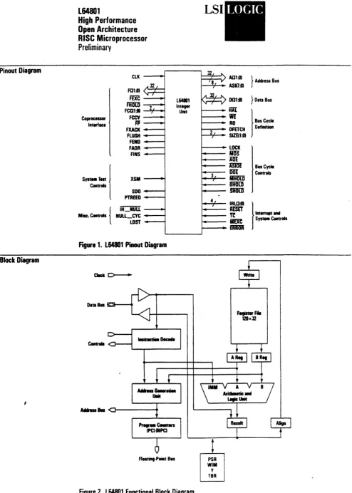
Features
L64801
LSI
High Performance
Open Architecture
RiSe
Microprocessor
Preliminary
The l64801 Integer Unit nU) is a high performance CMOS implementation of the SPARe (ScaJable Processor ARChitecture) 32 ·bit RISC microproces· sOt SPARC is an open architecture which is being implemented in a variety of forms by various semi·
conductor manufacturers. This multiple sourcing al· lows designers to choose from a wide variety of price/performance options and provides a rich see lection of peripherals. memory devices and proprio etary ASIC extensions.
The L6480 1 features a large register file to opti· mize procedure calls, variable assignments and context switches. Execution speed improves signif· icantJy because this register·to-register architec-ture minimizes the number of external memory accesses. Most of the l64801 instructions exe· cute in a single cycle due to its 4-stage pipeline that minimizes interlocks, a bus structure that al· lows single-cycle instruction/data accesses and an optimized branch handlet
• High performance operation
Commercial L64801C·20 l64801C·25 Military L64801M·15 l64801M·20 • Open architecture:
12 VAX MIPS
15 VAX MIPS 9 VAX MIPS 12 VAX MIPS - Mwtiple vendor sourced
- Each vendor provides unique features and extensions
- Variety of binary compatible price/performance options
• Optimized for operation under high·levet languages
such as C, FORTRAN, Pascal and Ada and the UNIXTM operating system
• External MMU, memory system and floating-point
unit assure flexible interface for the largest range of applications and price/performance levels
The l64801 can sustain 15 VAX MIPS perform-ance with peak performperform-ance of 25 MIPS, offer-ing designers the speed and power of a super minicomputet
L64801 Chip Photo • 32 ·bit virtual address bus
- Supports up to 4 Gbytes of direct address spa
- Allows a variety of memory management and caching schemes
• Simp'e instruction format with fast instruction cycle with a 4·stage pipeline
• Single cycle execution for the majority of instructions
• large central register file divided into seven overlapping windows of 24 registers each • All pipeline interlocks implemented directly in
hardware
• High performance coprocessor interface for
concurrent execution of floating-point or other coprocessor instructions
• Multitasking support with userlsupervlsor mode and privileged instructions
• Artificial intelligence support through use of tagg instructions
• Option to use as ASIC core
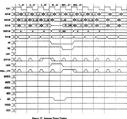
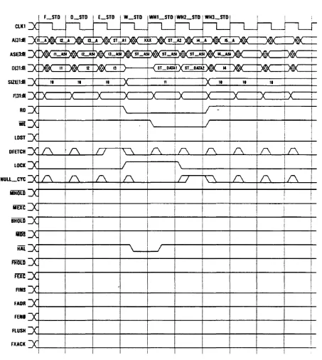
Pinout Diagram
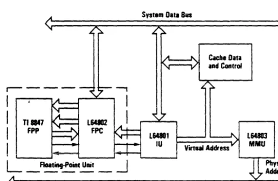
810ckDiagram
I:ligh Performance
Open Architecture
RiSe
Microprocessor
Preliminary
CLK
f(31:OJ
FEXC
FHOLD
Fca1:1
FCCV
f1S FXACK
FLUSH FEND FADA
RNS
~
Coproceaor Interlace
Syst_ TISt
I
Controls
XSM
SOO
PTREEO
l-7
Rgur.
1. L64801
Pinout DiagramData Bas ~-...
MIhsIa. c r - - - t
32" "
~
18, ...
I
A 32" ...
l64881 ~
Integer Unit
2"
I
3,
,
.
..
,I
A(31:O)
} Address Bus
ASI(7:O)
0(31:1) } Data Bus
til[
}=
fir AD ORTCH SlZEU:OI
LOCK
fim!
Am
Dm'E BusCyde
DOE Controls fiUR[ij
IIm'['D
!RiD
IRU3:OI
IBlT
TC
}---8m S~ Controls
Introduction
Architecture Overview
L64801
High Performance
Open
Architecture
RiSe Microprocessor
Preliminary
The l64801 is the first processor iii the LSI
lOQic familv of SPARe (Scalable Processor ARWChitecture) microprocessors. SPARC is an ar·
chitec;ture defined by Sun Microsystems which is
based on the principles of RISC (Reduced Instruc· tion Set Computer) techniques. The key feature of SPARC is its use of a large central register file which is divided into several "register windows" for high performance during subroutine caUs and context switching.
The SPARC family is supported by a full line of highJy optimizing compilers, operating systems,
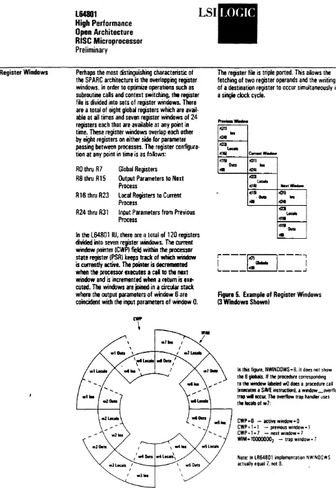
The l64801 SPARe chip set consists of a central integer unit UU) which provides all the core func· tions of the SPARC instruction set as defined by the SPARC architecture manual. To increase per·
formance of floating-point operations, there is an
optional floating-point unit (FPU) and a separate interface chip caned the floating-point controller (FPC).
The IU is the primary computing element. It
performs all operations except floating-point
op-erations (FPops) which are either performed in
hardware through the FPC/FPU combination, or in software. The FPC/FPU provides execution of FPops concurrent with integer operations.
The IU features a large central register file parti· tioned as sets of working registers (r registers) which provide storage for processes. In addition,
r
-I
I
TI8847I
FPPI ,
IL64801
IU
L
_Floating-Point Unit _.J
System Address Bus
Figure 4. SPARC System·Level Diagram
L!Sl
deveiopment boards, development systems and development tools.
SPARe is an open architectuie, built by a number
of semiconductor suppliers, which will provide
rapid enhancement of features for different mar· kets and a wide range of price/performance options. lSI logic has chosen to implement the
l6