Volume 4, No. 4, March-April 2013
International Journal of Advanced Research in Computer Science
RESEARCH PAPER
Available Online at www.ijarcs.info
ISSN No. 0976-5697
Power Harvesting and Area Efficient Clock Gating Method for a De-Composed MUX
Controller
R.G.Venkatesan*
P.G. Student, M.Tech – VLSI Design Bharath University Chennai,
India – 600073. [email protected]
S.Vijayakumar
Dept. of Electronics and Communication Engineering Ganadipathy Tulsi’s Jain Engineering College
Vellore, India – 632102. [email protected]
P.Yesodha
Dept. of Electronics and Communication Engineering Bharath University Chennai, India – 600073.
Abstract: Multiplexer (MUX) is the key switching element to process and feed the data to various blocks of a computing core. Nowadays the data size is of 64 bit or beyond. The use of MUX in ALU’s plays a prominent role to switch the correct logic path to further stage. Overall MUX architecture for a larger data width uses more number of transistors and consumes unnecessary stand by or static power. To reduce the static power consumption, the de-composed MUX with 2-1 MUX as a leaf cell is used as a tree like structure to build the top module. The Controller which utilizes the PTL clock gating concept consumes nearly 20 µW low power than the AND gate as clocking gate. However the simulation results show that the former one is nearly 100ns slower than the basic AND as clocking gate due to the so called trade off.
Keywords: Clock gating; low power; de-composed MUX; area optimization; dynamic; switching activity;
I. INTRODUCTION
The data paths of all the arithmetic circuits have the Multiplexers (MUX) for switching the data properly which are the complete 2n:1 MUXes in which all the transistors are always on and consume power. To eliminate this drawback, the decomposition method is applied to split the 2n:1 MUX into the tree of 2-1 MUXes which reduces the un-necessary power wasted by entire module [1].
In any MUX decomposition, the power consumed is given by the sum of the power consumed in all the MUXes in the tree. But different decompositions lead to different power consumptions [2]. Minimum power MUX decomposition is defined to be a MUX decomposition in which the power consumption is minimized. It uses a model of implementation of a 2-to-1 MUX where the power consumed is proportional to the switching activity and is the so called dynamic power dissipation expressed as pd ∞ ½(CLVDD2ƒ). Where, CL is the
load capacitance, VDD is the supply voltage and ƒ is the
frequency of circuit switching.
Hence, by reducing the switching activity yields the reduction in the dynamic power consumption. This is achieved by the following factors:
a. Dynamic activity controls like the application of clock gating
b. Find the paths which are switching unintended and control them
c. Use the efficient architecture which operates at low power
d. Utilize the power gating methods to reduce standby power as the sub 100nm circuits have the impact of it.
This paper deals the first three factors to implement which are appropriate to consider. The following few lines describe the organization of this paper. Section 2 says the sources responsible for power dissipation. The importance of device and technology impact on low power is given in section 3. In section 4, the unnecessary switching activity in a de-composed MUX tree is given along with the solution to reduce the redundant transition.
The controller architecture for dynamic activity reduction is also given. The existing and proposed clock control schemes are in section 5. The performance analyses of the two clock gating methods are available in the next section. Finally the work is concluded in section 7.
II. SOURCES OF POWER DISSPATION
Nowadays the power usage is an important factor than the area and speed of a design. This is because of the consumers taste of using portable devices like Lap-top computers, Personal Digital Assistants (PDA), cellular phones and many compact gadgets than the space occupying larger versions of those kind and results in less battery size with long back-up time to think about low operating power.
Hence the average power consumption has become a critical design issue to give less importance to speed with matching area. This situation causes to think about alternative battery material for long stand-by time.
d. Total power consumption
A. Battery power:
The battery operating power depends on the area and clock frequency of the circuit. This is expressed as
P = α.area.ƒclk (1)
Where,
P – power dissipation, α = 0.063W/cm2,
ƒclk – Clock frequency
As the clock frequency increases, the switching probability of the circuit also increases to cause more power consumption. The larger module area also effects in more power usage.
B. Switching Activity:
The power consumed by switching activity is considerably more and it varies among logic to logic [3]. This is due to the variation in switching probability or on probability (whenever there is a state change from logic ‘0’ to logic ‘1’). For example, if we take a NOR logic gate, the dynamic probability factor is 0.75, that is expressed as
PNOR= 0.75 CLVdd2ƒclk (2)
Where,
PNOR – Probability of NOR gate,
CL – Load Capacitance,
Vdd – Supply Voltage,
ƒclk – Clock frequency
On the other hand, the activity factor for the static NOR gate will be only 3/16.
C. Short Circuit Current:
Considerable rise and fall time of the input resulting in a direct path exists between Vdd and GND. This happens
whenever the input voltage falls between VTn < Vin < Vdd - |VTp|
and causes a conductive path between Vdd and GND. In such
situations, both NMOS and PMOS devices are on. This is the case for static design and impossible in a Dynamic approach because the Pre-charge and Evaluation are not occurring at the same time [3]. The NMOS device current is given by,
I = β/2(Vin- Vt)2 for 0 < I < Imax (3)
Where, β is the gain factor, Vin is the input voltage, Vt is the
threshold voltage and Imax is the maximum device current.
D. Total Power Dissipation:
Any Digital CMOS circuit may have three major sources of power dissipation namely Dynamic, Short circuit and Leakage power. Hence the total power consumed by any digital system can be estimated using the below expression
Ptot = Pdyn+ Psc+ Pleak
= CLVddVƒClk + ISCVdd + IleakVdd (4)
The first term Pdyn represents the switching component of
power, the next component Psc is the short circuit power and
Pleak is the leakage power. Where, CL is the loading
capacitance, ƒClk is the clock frequency which is actually the
probability of logic 0 to 1 transition occurs (the activity factor).
Vdd is the supply voltage, V is the output voltage swing which is
equal to Vdd; but in some logic circuits, such as pass-transistor
implementations, the voltage swing on some internal nodes may be slightly less than Vdd [4].
The current ISC in the second term is due to the direct-path
short circuit current which arises when both the NMOS and PMOS transistors are simultaneously active, conducting current directly from supply to ground [5].
Finally, the leakage current Ileak, which can arise from
substrate injection and sub-threshold effects, is primarily determined by fabrication technology considerations. This current is very much negligible and hence in most of the estimations it is practically not accounted. The dominant terms in a “well-designed” circuit are the switching component, Supply voltage and short circuit current. Thus for low-power design the important task is to minimize CL, Vdd, ƒClk while
retaining the required functionality.
III. DEVICE AND TECHNOLOGY IMPACT ON LOW POWER
This is about the impact of device and technology on a module for low power minimization. The threshold voltage, gate oxide thickness and technology scaling are the major techniques which make an impression on a circuit to be treated as low power module.
A. Effects of Vdd on Speed:
One of the effective way to reduce the CMOS Power is to reduce the Vdd because, the power is proportional to it. But this
results in lowering the gate speed. This can be rectified with the help of technology optimization. The gate delay for this optimization is expressed as
τ = CVdd[(1/Idsat n ) + (1/Idsat p)]/4 (5)
Where,
C – Capacitance,
Idsat n,p – Saturation current of NMOS and PMOS
transistors respectively.
Here, the time taken by NMOS to discharge the capacitor is from Vddto Vdd/2 and by PMOS to charge the capacitor is from
0 to Vdd/2.
B. Effects of Vt on Speed:
The reduction in threshold for a particular supply voltage causes the current saturation to increase and reduce the gate delay resulting in an increased speed of the circuit. The familiar mobility equation which explains the relationship between current, supply voltage, threshold voltage (Vt) and mobility of
charge careers is expressed as
Ids = µnCoxW[(Vgs-Vt)2]/2L (6)
Where,
Ids – Drain Current,
µn – Mobility of electrons,
Cox – capacitance of gate oxide,
W – Channel width,
Vgs – gate voltage,
The decrease in gate delay due to increased current flow can be understood from the relationship between them with the help of equation (5). Hence the reduction in threshold voltage can cause the increase in speed.
C. Transistor Sizing and Oxide Thickness:
As the channel width is varying, the capacitance of the device also changes and hence speed optimization is achieved. Hence the width of PMOS and NMOS devices will have a change to alter current, delay and speed of the circuit. These can be related with the help of the below expression.
Capacitance,
C = Cox + Cj + Cint
= α (Wn + Wp) + Cother (7)
Where,
Cj – junction capacitance,
Cint – internal capacitance of the device,
Wn,p – width of NMOS and PMOS.
IV. REDUNDANT TRANSITION, SWITCHING ACTIVITY REDUCTION AND CONTROLLER FOR
MUX TREE
This section describes the MUX tree implementation along with the switching activity reduction and clock gating concepts to optimize the power at a great extent [1]. The Complementary Static MUX which is the better choice for low power module among the static styles is chosen as low power 2-to-1 MUX to build the tree.
A. Traditional MUX Tree:
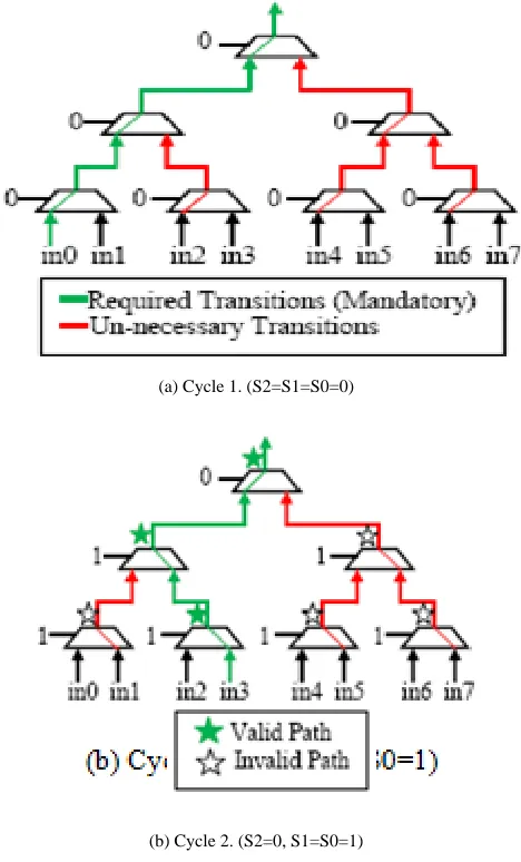
[image:3.612.335.569.78.465.2]Traditional 8-to-1 MUX tree is comprised of seven 2-to-1 MUX cells which is de-composed from 8-to-1 MUX as a single unit [6] – [9]. The property of this tree is that MUX cells in the same level share the same selection signal. There are three stages and hence S0, S1 & S2 are used as selection signals for level0, level1 & level 2 respectively. So, the selection signal S0 is connected to four MUX cells in the lowest level 0 as shown in figure 1. Because of this property, there are actually many unnecessary transitions within the tree.
Figure 1. Traditional MUX Tree.
To understand the control logic of a traditional tree, an example is given to identify those redundant transitions. In figure 2, assume that in0 is selected at the first cycle and in3 is selected at the second cycle. It this case, all the outputs of
MUX cells are altered at the second cycle because the selection signals of MUXes of lower two levels are all switched.
(a) Cycle 1. (S2=S1=S0=0)
(b) Cycle 2. (S2=0, S1=S0=1)
Figure 2. Redundant Transitions.
Even though in3 is correctly selected at last, all MUXes have output transitions. Actually, only the three transitions marked with green lines and “ ”are mandatory for the function correctness.
It is clear from figure 2(a) & 2(b) that there are many unnecessary MUX output transitions within a traditional MUX tree because MUXes at the same level share the same selection signal. Here, the MUXes other than the selection path are also having transitions from input to output which are actually of no use.
Some key draw backs are
a. The paths marked in red are not used for data propagation of the discussed case.
b. Data transition using this Shared Selection in a tree causes un-necessary switching power.
c. To eliminate this drawback, we need a controller which produces individual Select Signals to every MUX of all the tree stages.
[image:3.612.43.279.524.675.2]B. MUX Tree Architecture:
[image:4.612.55.280.162.385.2]This is a combination of the Controller and Tree structure. To minimize the unnecessary transitions of data due to selection signals, each MUX has its own independent selection input in our proposed architecture and a dedicated controller is responsible for generating individual selection control for each MUX as shown in figure 3. That is, the MUXes at the same level no longer share the same selection signal.
Figure 3. 8-1 MUX tree architecture
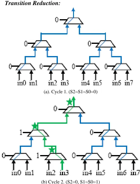
C. Transition Reduction:
(a). Cycle 1. (S2=S1=S0=0)
(b) Cycle 2. (S2=0, S1=S0=1)
Figure 4. Transition Reduction
For the Same Selection signal conditions as discussed in the traditional tree shown in Fig.2, only two MUXes get their selection signals changed at the second cycle, which leads to merely 3 MUX output transitions in total as shown in figure 4. The activity of the altered MUX tree is briefed as
a. Transition Reduction is achieved by keeping the Select logic of all MUXes to zero except the one which propagates.
b. As per the example, only two MUXes in the green path has the Select lines changed to Logic 1 and the others un-altered.
c. The switching power is reduced remarkably.
The tree architecture is hence capable of reducing the switching power of MUX selection signals as well as MUX outputs. This term is known as the popular switching activity reduction in the low power concepts. The power reduction happens in nodes and hence the dynamic power component which is due to the so called node transition activity is reduced drastically. This is the way to achieve dynamic power consumption.
D. Controller for transition reduction:
[image:4.612.335.566.398.541.2]Along with the independent selection signal for each MUX, another key idea of the proposed MUX tree architecture is that a controller is dedicated to generate proper selection signals for MUXes. The generated selection control must guarantee the correct functional behavior while minimizing the signal switches within the tree. The block diagram of the controller for an 8-to-1 MUX tree is shown in figure 5.
Figure 5. Controller for transition reduction
The controller takes the original 3-bit selection signal as input and produces a 7-bit output for independent MUX selection control. Registers are used to store the current values of selection signals. Based on the current input and register values, combinational logic determines the next 7-bit output with minimum possible number of transitions.
The function of the controller can be clear by seeing the propagation of data path between in0 to output. The controller with this condition of selection signals for an 8-to-1 MUX tree is shown in figure 6. To minimize the number of output transitions, the controller always keeps a MUX output unchanged if the function correctness can still be preserved no matter what the output value is.
[image:4.612.46.276.418.720.2]value. Precisely, whether the selection signal of a MUX must be properly set depends on whether that MUX lies on the path from the selected input to the tree output, named the output propagation path. For example, it is unnecessary to update S00 with mux_sel[0] unless the selected input is in0 or in1, i.e., mux_sel[2:1]= ‘00’. If it is not the case, S00 holds its previous value and the possible transition can then be eliminated. Similarly, S10 should be updated by mux_sel[1] only if mux_sel[2] = ‘0’. Since the root MUX always lies on the output propagation path no matter which data input is selected, S20 must be updated by mux_sel[2] every cycle.
Figure 6. MUX tree with controller
In simple words, if the selected data is in0, then only S20, S10 and S00 need to be properly set and the other four selection signals can just hold their previous values for maximum transition reduction.
E. Logic sharing between adjacent levels:
In a 2n-to-1 MUX tree, the value of mux_sel[n–1:k+1] determines whether a MUX, whose selection input is mux_sel[k], lies on the output propagation path or not. Hence it needs more complex combinational logic to decide whether the selection signals of lower level MUXes should be updated.
Figure 7(a) shows the controller without the sharing of select lines. It is observed that the decision logic is actually very similar between every two adjacent levels and thus significant logic sharing can be achieved as shown in Figure 7(b). The exploitation of logic sharing can effectively reduce both the area overhead and power dissipation induced by the controller.
[image:5.612.339.562.452.712.2]
(a). Without Selection Logic Sharing (b). With Selection Logic Sharing
Figure 7. Logic sharing between the adjacent levels
V. CLOCK GATING APPROACH TO THE CONTROLLER
The logic design shown in Figure 7 is capable of reducing the combinational logic power and minimizing output transitions of the registers, but the total power can still be lowered by further saving the register power. In a 2n-to-1 MUX tree, there are 2n–1 registers within the controller. Here only n registers at most change their values in a cycle. But the registers which do not change values still consume power because a running clock is present. Hence, the clock gating technique can be applied here to save power for those un-switched registers.
A. Types of clock gating:
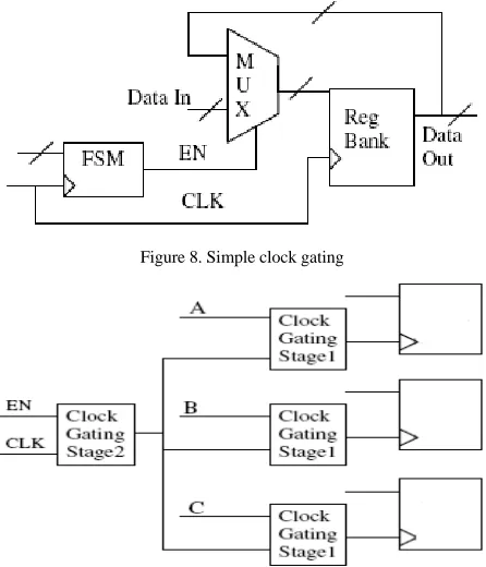
A group of flip flops of a same level shares a common clock gate is called a simple clock gating (clock gating is abbreviated as CG). CG is applied on register banks, which can be disabled during some clock cycles. Here a group of flip-flops that share the same clock and synchronous control signals and that are inferred from the same register bank [10] – [11].
Synchronous control signals include synchronous load enable, synchronous set, synchronous reset, and synchronous toggle. Without CG, synthesis tools in general implement register banks by using a feedback loop and a multiplexer as shown in figure 8.
Clock gating concept applied at the hierarchical level (Multi-stage) is named as complex clock gating. Complex CG can be applied at different hierarchical levels as shown in figure 9. Complex gating referred here are Module-Level, Enhanced, Multi-Stage, Hierarchical respectively. Minimum number of stages for multi-stage is 2 but higher number of stages can also be used if a design offers such hierarchical enable signals.
Figure 8. Simple clock gating
[image:5.612.43.281.543.695.2]B. Proposed Clock Gating scheme:
It is a method used to control the unnecessary switching power caused by flip flops as discussed a short while. The clock is gated to reduce the switching probability which is named as Clock Gating (CG) concept. It is one of the familiar Low Power approach. The paths with unchanged signal will not be propagated with this technique.
Various CG cells are shown in figure 10. The normal, un-gated flip – flop is shown figure 10(a). The conventional AND gate and the proposed Pass Transistor as CLK gating cell are shown in figure 10(b) & (c) respectively. These are taken for a comparison to decide which type is operating with low power. Figure 10(d) represents the CG applied flip-flop. The availability of CLK input is only when the EN signal is on. Hence at the un-changed data/signal, the switching activity is reduced.
(a) Un-gated flip-flop (b) AND gated clock signal
(b) Proposed – Pass Transistor as CG cell
[image:6.612.328.573.35.547.2](d) Clock gated flip-flop
Figure 10. Clock gating to flip – flop
VI. EXPERIMENTAL RESULTS
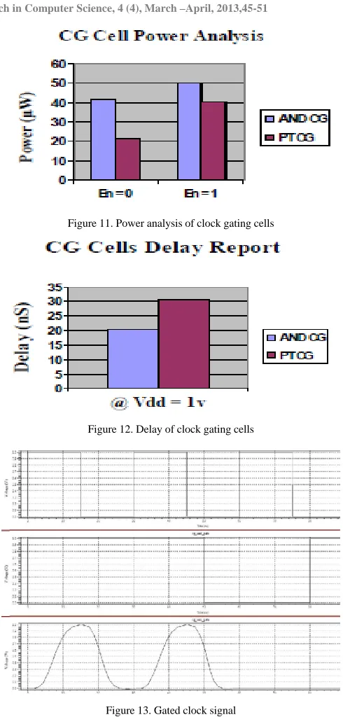
[image:6.612.48.251.250.449.2]The AND gated and Pass Transistor gated CG cells are simulated to find the low power cell. The power, delay and the PDP results are tabulated as in table I. The experimental results show that the gated power of PT CG is 48 % less than the AND CG cell. But the delay of AND CG cell is one tenth (1/10) smaller than the PT CG cell. This is due to the trade -off between parameters.
Table I. Analysis of Clock Gating Cells
@ Vdd = 1v Power (µW) Delay (nS)
En = 0 En = 1 En = 0 & 1
AND CG 41.789 50.085 59.36
Proposed PT CG 21.740 40.362 568.73
The comparison between the normal AND gate for clock gating and PT as CG cell has power and delay analysis. The power analysis is given in figure 11 while figure 12 represents delay. The gated clock signal is shown in figure 13.
[image:6.612.329.572.302.541.2]Figure 11. Power analysis of clock gating cells
Figure 12. Delay of clock gating cells
Figure 13. Gated clock signal
The proposed PT CG cell has dual advantages of low operating power and reduced area than the conventional AND gate as CG cell. It is because, in the case of power, the consumption is lesser due to few nodes of transition and hence reduced switching activity and small area with only 4 transistors to construct as against 6 transistors.
[image:6.612.50.275.598.654.2]VII.CONCLUSIONS
The MUX decomposition as a MUX tree is taken as the core architecture. The individual Selection Signal produced by controller minimizes the power consumed by node transition of the Architecture. This is not happened in the case of a Traditional tree. The efficient Controller avoids the un-necessary transitions at the nodes because of the discussed and exclusive selection lines. Due to the Controller Architecture, the circuit area seems to be increased which is a drawback. But the power optimization is the objective and increase in the area can be ignored due to trade-off.
Clock Gated Selection Signal produced by the controller minimizes the switching power of the Architecture. This is not happened in the gated design. The Controller avoids un-necessary transitions with the help of gating. With the use of the proposed PT CG as clock gating architecture, the circuit area is less than the conventional AND CG. The proposed one is an optimized approach in the sense of power too. These are achieved at the expense of speed which is not increased. Careful design metrics may improve it.
VIII.REFERENCES
[1] Nan-Shing Li, Juinn-Dar Huang, and Han-Jung Huang, “Low Power Multiplexer Tree Design Using Dynamic Propagation Path Control,” IEEE Asia Pacific Conf. on Circuits and Systems, Dec. 2008, pp. 838-841.
[2] U. Narayanan, H. W. Leong, K.-S. Chaung, and C. L. Liu, “Low Power Multiplexer Decomposition,” Int’l Symp. on Low Power Electronics and Design, 1997, pp. 269-274.
[3] A.Chandrakasan, R.W.Brodersen, “Low power Digital CMOS Design,” Kluwer Academic Publishers, 5th printing 2002.
[4] Rabaey M, Chandrakasan A, Nikolic B, “Digital Integrated Circuits – A Design Perspective,” Pearson Educational publishers – 2nd edition 2008.
[5] N.Weste, and K.Eshraghian, “Principles of CMOS VLSI design, a System perspective,” 2nd edition, Addison-Wesley,
1993.
[6] H.-E. Chang, J.-D. Huang, and C.-I. Chen, “Input selection encoding for low power multiplexer tree,” Int'l Symp. on VLSI Design, Automation, and Test, pp. 228-231, 2007.
[7] K. Kim, T. Ahn, S.-Y. Han, C.-S. Kim, and K.-H. Kim, “Low power multiplexer decomposition by suppressing propagation of signal transitions,” Int’l Symp. on Circuits and Systems, vol. 5, pp. 85-88, 2001.
[8] Sebastian T. Ventrone, “Low power multiplexer circuit,” United States Patent, Patent Number: 6,054,877, Apr. 2000.
[9] S.Vijayakumar, B.Karthikeyan, “An Efficient Low Power Static CMOS MUX Design for Multiplexer Trees,” Int. Conf. on Power, Signals, Control and Computations – EPSCICON, 2010.
[10] H.Mahmoodi, V.Tirumalashetty, M.Cooke, K.Roy, “Ultra Low-Power Clocking Scheme Using Energy Recovery and Clock Gating,” Vol. 17 (1), pp. 33-44, Jan. 2009.
[11] Rani Bhutada, Yiannos Manoli, “Complex Clock Gating with Integrated Clock Gating Logic Cell,” IEEE conf. ISBN No. 1-4244-1278-1/07, pp.164-169, 2007.
[12] Kaushik Roy, Sharad C.Prasad, “Low Power CMOS VLSI Circuit Design,” John Wiley & Sons, 2000.