High Gain DC-DC Converter with Coupled
Inductor for Photovoltaic Applications
Nimitha Gopinath
1, Aswathi S
2, Dr. Sheela S
3PG Student, Dept. of EEE, NSS College of Engineering, Palakkad, Kerala, India1 PG Student, Dept. of EEE, NSS College of Engineering, Palakkad, Kerala, India2 Professor, Dept. of EEE, NSS College of Engineering, Palakkad, Kerala, India3
ABSTRACT:Use of renewable energy is increasing day by day. Among them solar power is abundantly used nowadays. This results in the requirement of higher DC-DC voltage conversion for increasing output. Due to the lower voltage gain of various step up converters available, the efficiency of renewable systems are limited. This paper presents a switched coupled inductor dc-dc converter with high gain of 10. The designed circuit is simulated by MATLAB Simulink model and the results were verified by successfully building a prototype.
KEYWORDS: Photovoltaic (PV), DC-DC Converter, Switched coupled inductor
I. INTRODUCTION
Photovoltaic (PV) sources plays an important role in the world’s energy scenario and have potential to become the biggest contributions to the electricity generation among all other renewable energy sources by year 2050 because of its abundant availability[1]. The block diagram of photovoltaic system is shown in Fig 1.
Fig 1 Block diagram of photovoltaic system
II. RELATED WORK
1) Superliftluo converter
The voltage lift technique is a popular method that is widely applied in electronic circuit design [2]. The circuit diagram is as shown in Fig 2.
Fig 2Superliftluo converter
It has a high efficiency and a high power density. In addition, Super-Lift LuoConverter has the ability to reduce ripple voltage and current. But the voltage gain is 4.
1) High step up non isolated DC-DC converter
It does not limit current during overload conditions even though it limits the starting inrush current[3]. The voltage gain is 9.6. The circuit diagram is shown in Fig 3.
Fig 3 High step up non isolated DC-DC converter
2) Quadratic boost converter
Quadratic boost converter provides quadratic conversion ratio which offers wider conversion range[4]. As far as conversion efficiency is concerned, it is quite clear that a singlestage converter is always a better choice than a two-stage converter. Therefore, the quadratic converters are mainly used in applications where single-stage converters are required. The circuit diagram is shown in Fig 4.
Fig 4 Quadratic boost converter
Due the low voltage gain of the available converters, a new converter which is capable of high voltage conversion is to be analysed. There arises the importance of switched coupled inductor DC- DC converter.
III. SWITCHED COUPLED INDUCTOR DC-DC CONVERTER
Circuit diagram of the topology is as shown in Fig 5.
Fig 5 Switched coupled inductor DC-DC converter [3]
It consist of diode D1 and D2, coupled inductor, switch S1, magnetizing inductor Lm, capacitor C1, C2 and a
resistive load. The components in the converter are assumed to be ideal and capacitor value is large to withstand the high voltage [5]. For obtaining high gain, turns ratio is taken as 1:3. The magnetizing inductance is integrated into the primary winding N1 of coupled inductor T1. Parasitic resistance and the capacitance of the active switch and leakage
inductance are neglected. Operation of circuit consists of two modes. Mode I is shown in Fig 6.
Fig 6 Mode I [5]
Switch is kept in on position as shown in mode I. Here D2 will be reverse biased and D1 will be forward biased. Voltage passes to S1 through T1 and a part passes through D1, secondary winding of coupled inductor N1 and charges C1. This mode is called energy storage mode.
In mode II switch will not be a part of the circuit (Fig 7). D1 will be reverse biased and D2 will be in conduction mode. Therefore, the source Vin, Lm, C1and N2 winding are found to be in series and they charge the
capacitor C2 and the load. Hence this mode can be considered as energy releasing mode. So the total voltage conversion
ratio = 1+ voltage across T1 + Voltage across C1 + voltage across D2
Voltage conversion ratio = 1 +1 − 𝐷 +𝐷 1 + 𝑛1 +1 − 𝐷nD
= +𝑛−𝐷
−𝐷
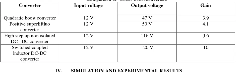
A comparison was made between various converters available with switched coupled inductor dc-dc converter on the basis of voltage gain is shown in Table 1.
Table 1
Comparison of various boost converters
Converter Input voltage Output voltage Gain
Quadratic boost converter 12 V 47 V 3.9 Positive superliftluo
converter
12 V 50 V 4.1
High step up non isolated DC –DC converter
12 V 116 V 9.6
Switched coupled inductor DC-DC
converter
12 V 120 V 10
IV. SIMULATION AND EXPERIMENTAL RESULTS
The Coupled inductor boost converter was analysed by MATLAB Simulink model. The circuit parameters for the simulation are listed in Table 2.
Table 2
Parameters and their values
PARAMETERS VALUES
Input voltage 12V
Output voltage 120V Switching frequency 50Hz Turns ratio of coupled inductor 1:3
Magnetising inductance 23uH Leakage inductance 0.32uH
Capacitor 1 100uF
Capacitor 2 22uF
Duty cycle 0.56
S1 IRF540
D1 BYQ2BE
D2 MUR860
Fig 8 MATLAB/SIMULINK model of Converter
Here series RLC branch is used a capacitors and load is selected as resistive. Pulse generator provide gating pulses to the switch. Fig.9 illustrates the output voltage of the converter. The curve represents the boosted output voltage with a value of 120V.
Fig 9 Output voltage of Switched coupled inductor dc-dc converter
In order to verify the circuit operation and confirm the simulation results a prototype is built and lab tested.
The input to the converter is provided from a 12V battery and is regulated by using LM7805. The controller is also supplied from the battery. The supply to the driver is provided through a 230/12 V adapter. Driver IC is selected as UCC27322 and controller IC is dsPIC30F2010. The overall hardware structure is shown in Fig 10.
V. CONCLUSION
Compared to basic converter topologies, switched coupled inductor dc- dc converter offers higher gain of value 10. The leakage inductor energy of the coupled inductor can be recycled and directly output to the load. This increases the
power conversion efficiency. Also, this converter consists of few components resulting in compact size and a high
power density can be achieved. All these can be efficiently utilized in photovoltaic applications. The designed circuit is simulated by MATLAB Simulink model and the results were verified by successfully building a prototype.
REFERENCES
[1] Wuhua Li, XiaodongLv, Yan Deng, Jun Liu, Xiangning He, “A Review of Non-Isolated High Step-Up DC/DC Converters in Renewable Energy Applications”, 978-1-422-2812-0/09/$25.00 ©2009 IEEE
[2] K.Prasanna, Dr.D.Kirubakaran, J.Rahulkumar, 4 J.A. Rudhran, “Implementation of Positive Output Super Lift Luo Converter for Photovoltaic System’, International Research Journal of Engineering and Technology (IRJET), Volume: 02 Issue: 03 | June-2015
[3] Wuhua Li, Xiangning He, “Review of Nonisolated High-Step-Up DC/DC Converters in Photovoltaic Grid-Connected Applications”, ieee transactions on industrial electronics, vol. 58, no. 4, april 2011
[4] K.H .Beena, Anish Benny, “Analysis and Implementation of Quadratic Boost Converter for Nanogrid Applications’, International Journal of Advanced Research in Electrical, Electronics and Instrumentation Engineering, Vol. 4, Issue 7, July 2015.
[5] Shih-Ming Chen, Man-Long Lao, Yi-Hsun Hsieh, Tsorng-Juu Liang, Kai-Hui Chen, “A Novel Switched-Coupled-Inductor DC–DC Step-Up Converter and Its Derivatives”, IEEE transactions on industry applications, vol. 51, no. 1, january/february 2015.
[6] G. Jessie GiftyJothi, Dr. N. Geetha,” An enhanced MPPT technique for high gain DC-DC converter for photovoltaic applications”, International Conference on Circuit, Power and Computing Technologies [ICCPCT],2016


![Fig 5 Switched coupled inductor DC-DC converter [3]](https://thumb-us.123doks.com/thumbv2/123dok_us/1574496.1193679/3.595.192.456.636.755/fig-switched-coupled-inductor-dc-dc-converter.webp)