using Sign Multiplier and Different Adder
Rahul Rochlani1, Sumit Dubey2, Anubhav Pandey3
M. Tech. Scholar, Department of Electronics and Communication, Jawaharlal Nehru College of Technology, Rewa,
Madhya Pradesh, India1
Assistant Professor, Department of Electronics and Communication, Jawaharlal Nehru College of Technology, Rewa,
Madhya Pradesh, India 2
Head of Department, Department of Electronics and Communication, Jawaharlal Nehru College of Technology, Rewa,
Madhya Pradesh, India 3
ABSTRACT: In this Technical era the high speed and low area of VLSI chip are very- very essential factors. Day by day number of transistors and other active and passive elements are drastically growing on VLSI chip. All the processors of the devices adders and multipliers are played an important role. Adder is a striking element for the designing of fast multiplier. Ultimately here need a fast adder for high bit addition. In this paper, the implemented of linear convolution are based on common Boolean logic and baugh multiplier. Proposing common Boolean logic (CBL) adder provides less components, less path delay and better speed compare to other existing CBL adder and other adders. Here we are comparing the linear convolution of different-different word size from other adders. The design and experiment can be done by the aid of Xilinx 6.2i Spartan device family.
KEYWORDS: Common Boolean Logic (CBL), Ripple Carry Adder Linear Convolution, Xilinx
I. INTRODUCTION
Now a days, time required in multiplication process is still the dominant factor in determining the instruction cycle time of a DSP chip [3]. Traditionally shift and add algorithm is being used for designing. However this is not suitable for VLSI implementation and also from delay point of view. Some of the important algorithms proposed in literature for VLSI implementable fast multiplication are Booth multiplier, array multiplier and Wallace tree multiplier [4]. Although these multiplication techniques have been effective over conventional “shift and add” technique but their disadvantage of time consumption has not been completely removed. Vedic Mathematics provides unique solution for this problem.
The Baugh-Wooley multiplication is one of the efficient methods to handle the sign bots. This approach has been developed in order to design regular multipliers, suited for 2‘s complement numbers [2]. Let two n-bit numbers, multiplier (A) and multiplicand (B), to be multiplied.
II. LITERATURE REVIEW
Rashmi K. Lomte et al., (2011, [1]), Convolution and Deconvolution has many applications in digital signal processing. Multipliers and dividers are basic blocks in convolution and deconvolution implementation. They consumes much of time. With advances in technology, many researchers have tried and are trying to design multipliers and dividers which offer either of the following- high speed, low power consumption, regularity of layout and hence less area or even combination of them in multiplier and divider. In this paper, direct method is used to find convolution and deconvolution. Discrete linear convolution of two finite length sequences using Urdhva Triyagbhyam algorithm is presented here. Same algorithm is also used for deconvolution to improve speed. This design approach efficiently and accurately speeds up computation without compromising with area.
Prof J M Rudagi et al., (2011, [2]), Multiplication is an important fundamental function in arithmetic operations. Multiplication-based operations such as Multiply and Accumulate(MAC) and inner product are among some of the frequently used computation Intensive Arithmetic Functions(CIAF) currently implemented in many Digital Signal Processing (DSP) applications such as convolution, Fast Fourier Transform(FFT), filtering and in microprocessors in its arithmetic and logic unit . Since multiplication dominates the execution time of most DSP algorithms, so there is a need of high speed multiplier. Currently, multiplication time is still the dominant factor in determining the instruction cycle time of a DSP chip.
Akhalesh K. Itawadiya et al. (2013, [3]), Digital Signal Processing (DSP) operations are very important part of engineering as well as medical discipline. Designing of DSP operations have many approaches. For the designing of DSP operations, multiplication is play important role to perform signal processing operations such as Convolution and Correlation. The new approach of this implementation is mentally and easy to calculate of DSP operations for small length of sequences. In this paper a fast method for DSP operations based on ancient Vedic mathematics is contemplated.
Surabhi Jain et al. (2014, [4]), In Digital Signal Processing, the convolution and deconvolution with a very long sequence is ubiquitous in many application areas. The basic blocks in convolution and deconvolution implementation
computing the multiplication of two numbers. The most significant aspect of the proposed method is the development of a multiplier and divider architecture based on Ancient Indian Vedic Mathematics sutras Urdhvatriyagbhyam and Nikhilam algorithm. The results show that the implementation of linear convolution and circular convolution using vedic mathematics is efficient in terms of area and speed compared to their implementation using conventional multiplier & divider architectures. The coding is done in VHDL. Simulation and Synthesis are performed using Xilinx ISE design suit 14.2
III. DIFFERENT TYPES OF ADDER
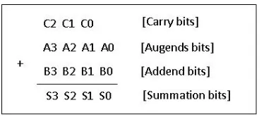
Ripple carry is a combinational circuit for adding more than two bit information. It is also called parallel adder. Ripple carry adder can be designed by using full adder in cascading form. Carry output of first full adder is connected with input of the next full adder, so carry is rippled from one adder to another adder. That is by it is called ripple-carry adder. Let us take example, for designing bit RCA inputs are and then carry
bits and summation bits are .
In this figure all the full adders are connected in cascading form. Carry input is an extra input which has fixed value . First full adder gives the carry output and summation output . Carry output of the first full adder is connected with second cascading full adder which will be considered as an input bit.
(1)
(2)
(3)
KOGGE STONE ADDER
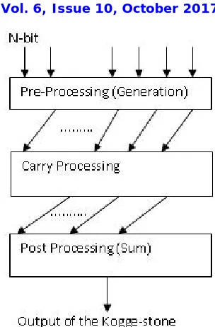
Kogge Stone Adder was proposed by Peter M. Kogge and Harold S. Stone. Kogge Stone Adder is an advanced technology of Look a- head Carry Adder. That is also called parallel prefix adder. It has more area than to Brent Kung Adder but less Fan-out. This adder provides the carry signal time and become fastest adder for industrial level.
First block of KSA is Pre- Processing that will generate and propagate the carry. Processing of carry will be done over the carry processing area and all the carry signal go through the post processing block. In the pre preprocessing stage we find the, generate and propagate signals from each inputs.
(4)
(5)
Carry processing stage provides the carries corresponding to each bit. Execution of these bit operation is carried out from parallel. After finding the carries in parallel they are segmented in to smaller pieces.
(6)
(7)
Bottom block is summation block which provides the summation bits. That blocks are comprised with XOR gate. If one input is different from another then output will be high. And if inputs are same then outputs will be low. Kogge Stone provides the less area than to other parallel adder like carry select adder, carry save adder and look ahead adder.
Above diagram is a functional diagram of Kogge Stone adder for 4 bit addition. Here elliptically symbol defined as a carry processing stage. The output of the preprocessing stage is fed to next carry stage and post processing as well.
MODIFIED COMMON BOOLEAN LOGIC ADDER
Area and power efficient high speed data logic path are the most significant areas of research. With the help of simple modification in gate level we can achieve the improvement in the results. Speed of the adder depends on the time required to propagate the carry through the adder. These adder works in series format, that is the sum of the elementary position bit is calculated when the previous bits are summed and the carry is propagated to that next stage.
Carry select adder (CSLA) is one of the advanced adders used in data processing processors to perform fast arithmetic function. It focuses on the problem of carry propagation delay by generating the carry independently at each stage and the select the efficient one with the help of multiplexer to perform the sum. The conventional CLSA is RCA (Ripple carry adder) which generate the partial sum and carry by using the input carry condition Cin=0 and Cin=1, select one out of each pair to form final sum and final carry output.
RCA is not area efficient as large number of gates circuitry is used to form the partial products and then the final sum and carry is selected.
Another form of CLSA adder uses binary to excess-1 convertor replacing ripple carry adder with Cin=1. This adder is known as CLSA along with BEC. The number of gates used has been reduced when we have to design large bit adder. This adders is more conventional as compare to RCA when deal with silicon area used but this is having marginally higher delay time.
The proposed Common Boolean Logic (CBL) adder is area-power-delay efficient. It work on the logic to remove the redundant adders and use Common Boolean Logic as compare to conventional carry select adder.
The CBL block is comprised of two parts sum generation block and carry generation block. In sum generation block the output sum is achieved using the multiplex. This multiplex is used to select the output value depeding on the value of Cin( previous bit).
If Cin=0, then output is xor of the two input bits. If Cin=1, then output get inverted. In carry generation block, multiplexer is used to select the carry of next stage depending upon the previous carry input. If Cin=0, cout is OR of two input and if Cin=1 the output carry is AND of the input bit.
Fig 4: A Functional Diagram of Kogge Stone Adder Stone Adder bit binary addition
B
AND
A
Carry
B
XOR
A
NOT
Sum
else
B
OR
A
Carry
B
XOR
A
Sum
C
If
in
)
(
0
This same process is used for the n number of bits and thus we get the final sum and carry as output.
IV. LINEAR CONVOLUTION
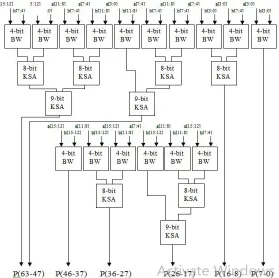
Complex logical designing can be reduced by the array mathematics calculation which is consisting with 16 sutras. Number of fan in, fan out pin and input output buffers can be minimized by using these array mathematics sutras. For the high speed convolution, multiplier and adder must be high efficient and low area as possible as. For instance (A3, A2, A1, A0) and (B3, B2, B1, B0) are the finite length sequence.
For the appropriate output we can use the 4 bit array multiplier, 8 and 9 bit Kogge Stone adder. Multiplication of convolution input sequence is different from ordinary binary multiplication.
propagation delay. Propagation delay must be less for better performance of digital circuit. Xilinx is an analysis and simulation tools which has many application in research filed. In this tool simulation is divided in to three categories, model, behavioral and structural. Xilinx 14.2i is an updated version which has many merits than other version.
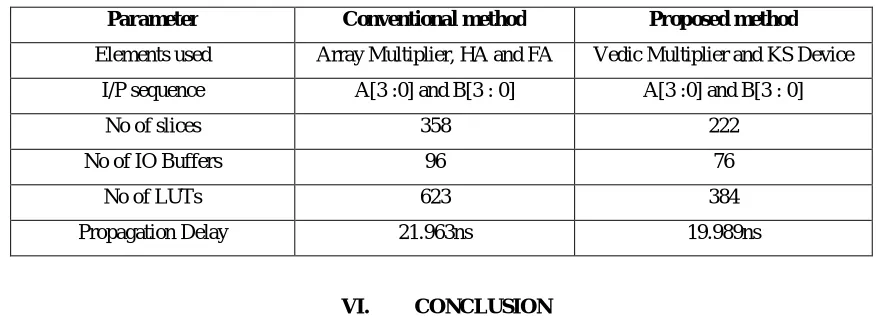
Table 1: Device Utilizations Summary of 4-input sequence high Speed Linear Convolution
Parameter Conventional method Proposed method
Elements used Array Multiplier, HA and FA Vedic Multiplier and KS Device
I/P sequence A[3 :0] and B[3 : 0] A[3 :0] and B[3 : 0]
No of slices 358 222
No of IO Buffers 96 76
No of LUTs 623 384
Propagation Delay 21.963ns 19.989ns
VI. CONCLUSION
Conclusion of this paper is that, designed a low power and less area or minimum propagation delays KSA Adder. According above table (see Table 1) ripple carry adder and other parallel adder has more number of slices than to KSA. Proposing high efficient KSA adder can be used for baugh multiplication to design high speed linear convolution. Apart from that it can be used in high speed convolution methods all the experiment has done in Spartan, Xilinx 6.2I VHDL package.
VII. FUTURE SCOPE
Now a day’s all the devices need a design with compact and high speed portable components. KSA adder can used to design a fast multiplier and multiplier is an important device for high speed processor. These devices can be used in high efficient convolution and de-convolution, FIR filter, ALU etc.
REFERENCES
[1] Jain, S. ; Saini S. “High Speed Convolution and Deconvolution algorithm (Based on Ancient Indian Vedic Mathematics) electrical engineering/electronics, computer, telecommunication and information technology (ecti-con), 2014 11th international conference on doi: 10.1109/ ecticon.2014.6839756 Publication Year: 2014 , Page(s): 1 – 5.IEEE 2014.
[2] Lomte, Rashmi K., and P. C. Bhaskar. ”High Speed Convolution and Deconvolution Using Urdhva Triyagbhyam.” VLSI (ISVLSI), 2011 IEEE Computer Society Annual Symposium on. IEEE, 2011.
[3] Itawadiya, Akhalesh K., et al.”Design a DSP operations using vedic mathematics.” Communications and Signal Processing (ICCSP), 2013 International Conference on. IEEE, 2013.
[4] L. Sriraman, T.N. Prabakar, “Design and Implementation of Two Variable Multiplier Using KCM and Vedic Mathematics,” 1st Int. Conf. on Recent Advances in Information Technology, Dhanbad, India, 2012, IEEE Proc., pp. 782-787.
[5] Soma BhanuTej, 2012.Vedic Algorithms to develop green chips for future, International Journal of Systems, Algorithms and Applications, Volume 2, Issue ICAEM12, ISSN Online: 22772677..
[6] Youngjoon Kim and Lee-Sup Kim, 2001.A low power carry select adder with reduced area, IEEE International Symposium on Circuits and Systems, vol.4, pp.218-221. Tavel, P. 2007 Modeling and Simulation Design. AK Peters Ltd.