ABSTRACT
DEMIRCIOGLU, HARUN. Modeling Layout Dependent Stress Effects for CMOS. (Under the direction of Dr. W. Rhett Davis.)
Process induced mechanical stress has enabled continued CMOS scaling since the
90nm node to improve carrier transport and maintain high drive current. This stress depends
strongly on the layout shape as well as the surroundings of each transistor in a circuit. The
resulting stress variation changes the individual transistor performance and circuit delay
which lead to yield loss. Therefore, analytical stress models are needed to relate these stress
dependent variations to critical layout parameters for design optimization.
This dissertation presents the development of accurate, non-process specific analytical stress
models which are capable of analyzing systematic layout induced mechanical stress
variations. The process and layout dependence of all relevant process induced intentional and
unintentional stress sources has been incorporated into our analytical models. Intentional
stress sources are embedded lattice mismatch stressors (LMS) and contact etch-stop liners
(CESL), whereas unintentional ones are shallow trench isolation (STI) and through silicon
via (TSV) stress.
Analytical models are calibrated and verified against silicon ring oscillator frequency
data. The models exhibit a very good fit to the silicon data and resulting root mean square
error (RMSE) between silicon and model results is less than 0.8%.
The created analytical models can be employed by circuit and layout designers to quickly
optimize their layout and reduce stress dependent performance degradations without using
© Copyright by Harun Demircioglu
Modeling Layout Dependent Stress Effects for CMOS
by
Harun Demircioglu
A dissertation submitted to the Graduate Faculty of North Carolina State University
in partial fulfillment of the requirements for the Degree of
Doctor of Philosophy
Electrical Engineering
Raleigh, North Carolina
2013
APPROVED BY:
_______________________________ ______________________________ Dr. Mehmet C. Ozturk Dr. Naiuhan Jing
_______________________________ ______________________________
DEDICATION
BIOGRAPHY
Harun Demircioglu was born on 28th October 1984, in Istanbul, Turkey. He received his Bachelor of Science (BS) degree with High Honors in Electrical and Electronics
Engineering, from Bogazici University, Istanbul, Turkey in Spring 2007. After graduating, he
moved to Raleigh, NC to continue his academic studies in North Carolina State University
Electrical and Computer Engineering Department. Harun started working towards his Ph.D.
degree in Fall 2007 and joined the research group “Methodologies for User-Friendly
System-On-A-Chip Experimentation” (MUSE) under the guidance of Dr. W. Rhett Davis in Spring
2008.
During his Ph.D., he worked as a graduate technical intern at Intel Corporation in Design for
Manufacturability (DFM) Group from January 2013 to July 2013, in Santa Clara, CA.
His research interests include modeling layout-dependent variations in CMOS transistors;
including stress effects and lithography imperfections, design for manufacturability and
ACKNOWLEGEMENTS
First of all, I would like to thank my advisor Dr. W. Rhett Davis, for believing into my
potential and giving me the opportunity working with him. He provided me guidance as well
as freedom and encouraged me to pursue my own ideas in conducting my research. Apart
from being a great advisor, he has been a good friend to me during my Ph.D. years. I have
always enjoyed having conversations with him.
I would like to thank Dr. Ozturk, who provided crucial support and friendship since I arrived
in Raleigh. I am also grateful to my committee members, Dr. Paul D. Franzon and Dr.
Naihuan Jing for agreeing on my thesis committee and for their valuable suggestions and
comments.
I would like to appreciate Dr. Joseph Tracy and Dr. Douglas L. Irving who served as
substitute members in my preliminary and oral defense exams.
I would like to thank all my colleagues who created a great academic and social environment
at NC State University.
I would like to acknowledge Mentor Graphics, Semiconductor Research Corporation (SRC)
and National Science Foundation (NSF) for their support to continue my research.
I would also like to thank Dassault Systèmes for generously providing access to the Abaqus
simulator used heavily in this work.
Finally, my special thanks to my dear family; my mother Nuran, my father Temel and my
TABLE OF CONTENTS
LIST OF TABLES ... ix
LIST OF FIGURES ... x
Chapter 1 Introduction ... 1
1.1 Motivation ... 1
1.2 Basics of Engineering Mechanics ... 3
1.3 Basics of Finite Element Method (FEM) ... 5
1.4 Stress Sources in CMOS ... 6
1.5 Strained Silicon Physics ... 9
1.5.1 Hole Mobility Enhancement under Stress ... 10
1.5.2 Electron Mobility Enhancement under Stress ... 10
1.6 Electrical Effects of Stress in CMOS ... 11
1.7 Previous Research in the Area of Stress Modeling ... 14
1.8 Original Contributions ... 16
1.9 Organization ... 18
References ... 19
Chapter 2 Modeling Stress for Lattice Mismatch Material in Junction Regions ... 25
2.1 Introduction ... 25
2.2 Technical Approach ... 27
2.2.1 FEM Modeling of an Isolated Transistor ... 29
2.2.1.1 Modeling LMS-Si Interface ... 32
2.2.1.2 Mesh and Boundary Conditions ... 33
2.3 Simulation and Modeling Results of Layout Sensitivity in an Isolated Transistor ... 33
2.3.1 Effect of Lattice Mismatch Stressor Concentration ... 38
2.3.2 Effect of LMS Recess Depth ... 42
2.3.3 Effect of Dopant Concentration ... 49
2.3.4 Effect of Raised LMS ... 52
2.3.5 Effect of Source and Drain LMS Spacing ... 56
2.3.6 Effect of Gate Height and Length ... 62
2.3.7 Effect of Spacer Length ... 64
2.3.8 Effect of Device Width ... 65
2.3.9 Effect of Recess Shape ... 72
2.3.10 Effect of Gate Stack ... 76
2.3.11 SOI vs. Bulk technology ... 86
2.5 Summary ... 87
References ... 89
Chapter 3 Modeling Stress for Contact-Etch Stop Liners ... 93
3.1 Introduction ... 93
3.2 Technical Approach & FEM Modeling of CESL ... 96
3.2.1 Mesh and Boundary Conditions ... 100
3.2.2 Virtual Splitting of CESL ... 101
3.3 Simulation and Modeling Results of Layout Sensitivity in an Isolated Transistor ... 103
3.3.1 Effect of CESL Intrinsic Stress ... 109
3.3.2 Effect of CESL Thickness ... 111
3.3.3 Effect of Spacer Width ... 115
3.3.4 Effect of Channel Length ... 119
3.3.5 Effect of Raised Diffusion Areas ... 122
3.3.6 Effect of Gate Height ... 126
3.3.7 Effect of Device Width ... 130
3.3.8 Effect of Contact Holes ... 133
3.3.9 Effect of Gate Stack ... 135
3.4 Parameter Ranges for DSL Models ... 138
3.5 Summary ... 139
References ... 141
Chapter 4 Modeling Stress for Shallow Trench Isolation ... 143
4.1 Introduction ... 143
4.2 Technical Approach & FEM Modeling of STI ... 144
4.2.1 Calculation of STI Stress for a Device ... 148
4.3 Simulation and Modeling Results ... 150
4.3.1 Effect of Length of Diffusion (LOD) ... 151
4.3.2 Effect of STI Length ... 153
4.3.3 Effect of STI Depth ... 154
4.3.4 Effect of Diffusion Width ... 156
4.3.5 Effect of Temperature Cycle ... 159
4.3.6 Effect of Oxide Deposition Method ... 160
4.4 Parameter Ranges for STI Models ... 163
4.5 Summary ... 164
References ... 165
Chapter 5 Modeling Stress for Contextual Effects ... 167
5.1 Introduction ... 167
5.3 Simulation and Modeling Results ... 170
5.3.1 Dense Device Modeling ... 170
5.3.1.1 LMS Dense Device Modeling ... 173
5.3.1.1.1 Effect of First Neighboring Junction ... 172
5.3.1.1.2 Effect of Second Neighboring Junction ... 176
5.3.1.2 CESL Dense Device Modeling ... 179
5.3.2 Modeling of Stress for Neighboring Active Area Effects ... 180
5.3.2.1 CESL Neighboring Active Area Modeling ... 181
5.3.2.1.1 Neighboring Active Area in Horizontal (x) Direction ... 181
5.3.2.1.1.1 Neighboring Active Area in the Same Well ... 182
5.3.2.1.1.2 Neighboring Active Area in different Well-(DSL Boundary Proximity Effect) ... 184
5.3.2.1.2 Neighboring Active Area in Perpendicular (y) Direction ... 188
5.3.3 Modeling of Stress for Active Jog Effects ... 189
5.4. Summary ... 192
References ... 194
Chapter 6 Modeling Stress for Through Silicon Vias (TSVs) ... 196
6.1 Introduction ... 196
6.2 Technical Approach & FEM Modeling of STI Stress ... 198
6.3 Model Development for a Single TSV ... 200
6.4 Simulation and Modeling Results for a Single Copper TSV ... 203
6.5 Summary ... 207
References ... 208
Chapter 7 Analytical Model Construction and Validation ... 210
7.1 Introduction ... 211
7.2 Analytical Model Construction ... 211
7.2.1 Parameter Sampling ... 211
7.2.2 Multidimensional Model Creation ... 213
7.2.3 Executable Analytical Models ... 218
7.3 Model Validation ... 219
7.4 Summary ... 223
References ... 224
Chapter 8 Conclusion and Future Work ... 225
8.2 Future Work ... 228
8.2.1 Stress Extractor Tool ... 228
8.2.2 Stress Models for Tri Gate-Transistors ... 229
LIST OF TABLES
Table 1.1 Piezoresistance coefficients for <110> channel orientation on (001) wafer. . 12
Table 2.1 Lattice Constants of Materials. ... 29
Table 2.2 Material Properties at Room Temperature. ... 29
Table 2.3 Parameter Explanations for Figure 2.1. ... 31
Table 2.4 LMS types and resulting Stress Types for all directions. ... 34
Table 2.5 Layout and Process Parameter Ranges for the LMS modeling. ... 86
Table 3.1 CESL type and resulting Stress Types for all directions. ... 96
Table 3.2 Parameter Explanations for Figure 3.4. ... 99
Table 3.3 Material Properties at Room Temperature. ... 100
Table 3.4 Layout and Process Parameter Ranges for the DSL modeling. ... 139
Table 4.1 Parameter Explanations for Figure 4.1. ... 147
LIST OF FIGURES
Figure 1.1 Stress components on the surfaces of an infinitesimal cube. ... 3
Figure 1.2 Deformation of a spring with an applied Force. ... 4
Figure 1.3 Desired Stress Types for CMOS Transistors. ... 7
Figure 1.4 Mechanical Stress Sources in CMOS Transistors. ... 7
Figure 1.5 Mobility Enhancement (μ/μ0) vs. Parallel Stressσ11(=SXX) for Uniaxial compression in the direction of [110] on (001) Si wafer. ... 13
Figure 1.6 Stress Advisor Flow. ... 17
Figure 2.1 Transistor structure with Lattice Mismatched Stressor for FEM simulation. ... 30
Figure 2.2 Si- Si1-xGex Interface. ... 32
Figure 2.3 Directions of Stress. ... 34
Figure 2.4 Parallel Stress Distribution along Transistor Channel for different Si1-xGex Spacings (LLMS). ... 36
Figure 2.5 Simulated and Modeled Parallel Stress vs. Diffusion Length (LS/D) for different STI Lengths (LSTI). ... 37
Figure 2.6 Simulated and Modeled Parallel Stress vs. STI Length (LSTI) for different Diffusion Lengths (LS/D). ... 37
Figure 2.7 Lattice Mismatch Strain vs. LMS concentrations. ... 39
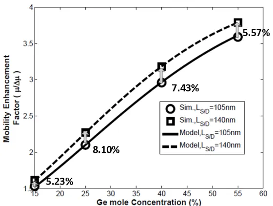
Figure 2.8 Simulated and Modeled Stress vs. Diffusion Length (LS/D) for different Ge Concentrations. ... 40
Figure 2.9 Mobility Enhancement Factor vs. Ge mole Concentration for different Diffusion Lengths (LS/D). ... 41
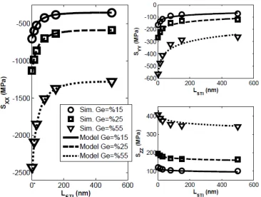
Figure 2.10 Simulated and Modeled Stress vs. STI Length (LSTI) for different Ge Concentrations. ... 42
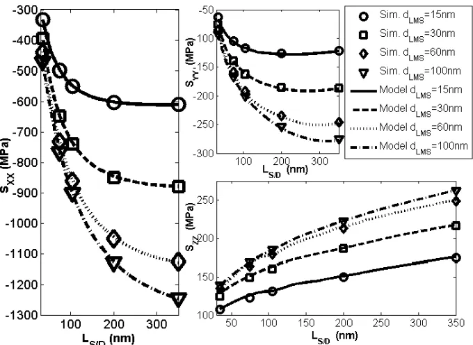
Figure 2.11 Simulated and Modeled Stress vs. Diffusion Length (LS/D) for different Recess Depths (dLMS). ... 43
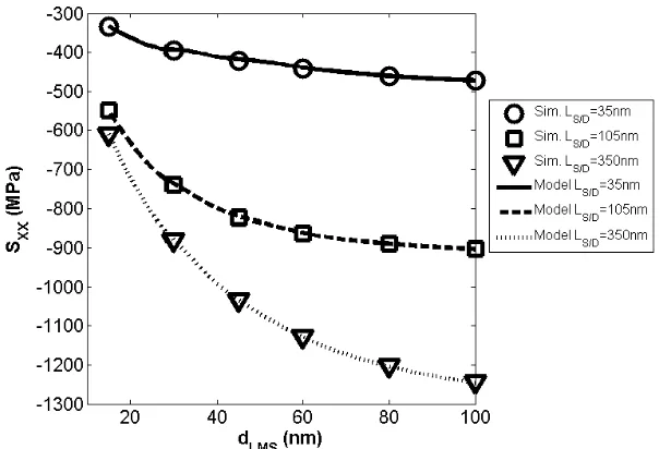
Figure 2.12 Simulated and Modeled Parallel Stress vs. Recess Depth (dLMS) for Diffusion Lengths (LS/D). ... 44
Figure 2.13 Simulated and Modeled Parallel Stress vs. STI length (LSTI) for different Recess Depths (dLMS). ... 45
Figure 2.14 Simulated and Modeled Stress vs. Recess Depth (dLMS) for different STI lengths (LSTI). ... 46
Figure 2.15 Distance in z-direction vs. Displacement of Si1-xGex junction with very short STI for Recess Depths (dLMS). ... 47
Figure 2.16 Distance in z-direction vs. Displacement of Si1-xGex junction with long STI for Recess Depths (dLMS). ... 48
Figure 2.18 Simulated and Modeled Stress vs. Diffusion Length (LS/D) for different
Boron Concentrations. ... 51 Figure 2.19 Simulated and Modeled Stress vs. STI Length (LSTI) for different Boron
Concentrations. ... 52 Figure 2.20 Simulated and Modeled Stress vs. Diffusion Length (LS/D) for different
LMS Raised Junction Heights (hLMS). ... 53
Figure 2.21 Simulated and Modeled Stress vs. STI Length (LSTI) for different LMS
Raised Junction Heights (hLMS). ... 54
Figure 2.22 Simulated and Modeled Parallel Stress vs. LMS Raised Junction Height (hLMS) for Recess Depths (dLMS). ... 55
Figure 2.23 Simulated and Modeled Stress vs. Diffusion Length (LS/D) for different
Stressor Spacings (LLMS). ... 57
Figure 2.24 Simulated and Modeled Stress vs. STI Length (LSTI) for different Stressor
Spacings (LLMS). ... 58
Figure 2.25 Simulated and Modeled Parallel Stress vs. Recess Depth (dLMS) for
different Stressor Spacing (LLMS) and STI Lengths (LSTI). ... 60
Figure 2.26 Simulated and Modeled Parallel Stress vs. LMS Raised Junction Height (hLMS) for different Stressor Spacings (LLMS). ... 61
Figure 2.27 Simulated and Modeled Parallel Stress vs. Stressor Spacing (LLMS) for
different Boron Concentration. ... 62 Figure 2.28 Simulated and Modeled Stress vs. Gate Height (hGATE) for different Gate
Lengths (LGATE). ... 63
Figure 2.29 Simulated and Modeled Stress vs. Spacer Width (LSPACER) for different
Gate Lengths (LGATE). ... 65
Figure 2.30 Top view of a device structure in a 2-D layout context. ... 66 Figure 2.31 Simulated and Modeled Stress vs. Device Width for different Recess
Depths (dLMS). ... 67
Figure 2.32 Lattice Structure for Wide and Narrow Width Devices. ... 68 Figure 2.33 Simulated and Modeled Mobility Enhancement Factor vs. Device Width
(W) for different Recess Depths (dLMS). ... 70
Figure 2.34 Simulated and Modeled Parallel Stress vs. Device Width for different
Stressors Spacing (LLMS). ... 70
Figure 2.35 Simulated and Modeled Stress vs. STI_Y Length (LSTI-Y) for different
Device Widths (W). ... 71 Figure 2.36 Simulated and Modeled Stress vs. Diffusion Length (LS/D) for Σ and
U-shaped LMS with different Recess Depths (dLMS). ... 73
Figure 2.37 Simulated and Modeled Stress vs. Diffusion Length (LS/D) for Σ and
U-shaped LMS with different Stressor Spacings (LLMS). ... 74
Figure 2.38 Simulated and Modeled Parallel Stress vs. STI Length (LSTI) for Σ and
U-shaped LMS with (a) different Recess Depths (dLMS), (b) different Stressor
Spacing (LLMS). ... 75
Figure 2.40 Simulated and Modeled Parallel Stress vs. Young’s Modulus of Gate for
different Recess Depths (dLMS). ... 78
Figure 2.41 Simulated and Modeled Parallel Stress vs. Young’s Modulus of Gate for different Gate Lengths (LGATE). ... 79
Figure 2.42 Simulated and Modeled Stress vs. Diffusion Length (LS/D) for different Gate Stacks. ... 81
Figure 2.43 Simulated and Modeled Stress vs. STI Length (LSTI) for different Gate Stacks. ... 82
Figure 2.44 Illustration of Approaches for Metal Gate with Polysilicon Capping Layer. ... 83
Figure 2.45 Simulated and Modeled Parallel Stress vs. TiN Height for Tin+Poly Gate Process for different Gate Lengths (LGATE). ... 83
Figure 2.46 Simulated and Modeled Parallel Stress vs. TiN Height for two processes; TiN+Poly Gate and Tin+Removed Poly Gate. ... 85
Figure 3.1 DSL Process Flow. ... 94
Figure 3.2 Directions of Stress. ... 95
Figure 3.3 CESL Intrinsic Stress Directions. ... 97
Figure 3.4 2-D and 3-D Isolated Transistor structures with CESL for FEM simulation. ... 98
Figure 3.5 Virtual Splitting of CESL. ... 102
Figure 3.6 Parallel and Vertical Stress Distribution Along Transistor Channel for a Tensile CESL of 1GPa. ... 104
Figure 3.7 Simulated and Modeled Stress vs. Diffusion Length (LS/D) for all Separate Regions of CESL and the Complete CESL. ... 106
Figure 3.8 Simulated and Modeled Parallel Stress for Complete CESL vs. Diffusion Length (LS/D) for different STI Lengths (LSTI). ... 107
Figure 3.9 Simulated and Modeled Stress vs. STI Length (LSTI) for all Separate Regions of CESL and the Complete CESL. ... 108
Figure 3.10 Simulated and Modeled Parallel Stress for Complete CESL vs. STI Length (LSTI) for different Diffusion Lengths (LS/D). ... 109
Figure 3.11 Simulated Complete CESL Stress vs. CESL Intrinsic Stress. ... 110
Figure 3.12 CESL thickness. ... 111
Figure 3.13 Simulated and Modeled Stress vs. CESL Thickness (hLINER) for all Separate Regions of CESL and the Complete CESL. ... 113
Figure 3.14 Simulated and Modeled Parallel Stress for Complete CESL vs. Diffusion Length (LS/D) for different Liner Thicknesses (hLINER).. ... 114
Figure 3.15 Simulated and Modeled Parallel Stress for Complete CESL vs. STI Length (LSTI) for different CESL Thicknesses (hLINER). ... 114
Figure 3.17 Simulated and Modeled Stress for Complete CESL vs. Diffusion Length
(LS/D) for different Spacer Widths (LSP).. ... 117
Figure 3.18 Simulated and Modeled Stress for Complete CESL vs. Spacer Width (LSP). for different CESL Thicknesses (hLINER). ... 118
Figure 3.19 Simulated and Modeled Stress vs. Gate Length (LCH) for all Separate Regions of CESL and the Complete CESL. ... 119
Figure 3.20 Simulated and Modeled Parallel Stress for Complete CESL vs. Diffusion Length (LS/D) for different Gate Lengths (LGATE (=LCH)).. ... 120
Figure 3.21 Simulated and Modeled Stress for Complete CESL vs. Gate Length (LGATE (=LCH)). for different Spacer Widths (LSP). ... 121
Figure 3.22 Lateral Liner Height. ... 122
Figure 3.23 Simulated and Modeled Stress vs. Junction Step Height (hS/D) for all Separate Regions of CESL and the Complete CESL. ... 123
Figure 3.24 Mobility Improvement (Δμ/μ) Loss vs. Junction Step Height (hS/D). ... 124
Figure 3.25 Simulated and Modeled Parallel Stress for Complete CESL vs. Diffusion Length (LS/D) for different Junction Step Heights (hS/D). ... 125
Figure 3.26 Simulated and Modeled Stress vs. Gate Height (hGATE) for all Separate Regions of CESL and the Complete CESL. ... 126
Figure 3.27 Simulated and Modeled Stress vs. Gate Height (hGATE) for Top Liner for different CESL Thickness and Gate Length Combinations (hLINER, hGATE). ... 128
Figure 3.28 Simulated and Modeled Parallel Stress for Complete CESL vs. Diffusion Length (LS/D) for different Gate and Junction Step Height Combinations (hGATE, hS/D). ... 129
Figure 3.29 A quarter of an isolated transistor in 3-D. ... 130
Figure 3.30 Simulated and Modeled Stress for Complete CESL vs. Device Width (W).. ... 131
Figure 3.31 Mobility Improvement (Δμ/μ) Change vs. Device Width (W). ... 132
Figure 3.32 Simulated and Modeled Parallel Stress vs. Square Contact Hole Width for Bottom Liner for different Diffusion Lengths (LS/D). ... 134
Figure 3.33 Simulated and Modeled Parallel Stress vs. Contact Distance from Spacer Edge for Bottom Liner for different Number of Contacts. ... 135
Figure 3.34 Simulated and Modeled Stress vs. Young’s Modulus of Gate Material for all Separate Regions of CESL and the Complete CESL. ... 136
Figure 3.35 Simulated and Modeled Stress vs. TiN Height for Tin+Poly Gate Process for all Separate Regions of CESL and the Complete CESL. ... 137
Figure 4.1 Layout View and 3-D FEM Model for STI stress simulation. ... 146
Figure 4.2 Layout Parameters for STI Stress Calculation. ... 149
Figure 4.3 Simulated and Modeled STI Stress vs. Length of Diffusion (LOD). ... 151
Figure 4.5 Simulated and Modeled STI Stress vs. Length of STI (LSTI). ... 153
Figure 4.6 Simulated and Modeled STI Stress vs. Distance from STI/Si edge for different Lengths of STI (LSTI). ... 154
Figure 4.7 Simulated and Modeled STI Stress vs. Depth of STI (dSTI). ... 155
Figure 4.8 Simulated and Modeled STI Stress vs. Distance from STI/Si edge for different depths of STI (dSTI). ... 156
Figure 4.9 Simulated and Modeled STI Stress vs. Width of Diffusion (W) for different STI lengths in y-direction (LSTI_Y). ... 157
Figure 4.10 % Mobility Improvement (Δμ/μ) Change vs. Width of Diffusion (W) for PMOS & NMOS. ... 158
Figure 4.11 Simulated and Modeled STI Stress vs. Process Temperature Change (ΔT). ... 160
Figure 4.12 Simulated and Modeled STI Stress vs. Initial STI Stress for different STI Lengths (LSTI). ... 162
Figure 4.13 Simulated and Modeled STI Stress vs. Initial STI Stress for different STI depths (dSTI). ... 163
Figure 5.1 FEM simulation categories. ... 169
Figure 5.2 Directions of Stress. ... 169
Figure 5.3 Dense Device and its equivalent Stress Layout. ... 171
Figure 5.4 Non-uniform Neighboring Effect in Width direction. ... 172
Figure 5.5 Device Layout with First Neighboring Junction. ... 173
Figure 5.6 Simulated and Modeled Paralel Stress vs. First Neighboring LMS Length (LSIGE_2) for different Recess Depths (dLMS). ... 174
Figure 5.7 Simulated and Modeled Paralel Stress vs. First Neighboring LMS Length (LSIGE_2) for different LMS Lengths (LSIGE_1). ... 175
Figure 5.8 Simulated and Modeled Parallel Stress vs. STI Length (LSTI) for different First Neighboring LMS Lengths (LSIGE_2). ... 175
Figure 5.9 Device Layout with Second Neighboring Junction. ... 176
Figure 5.10 Simulated and Modeled Parallel Stress vs. Second Neighboring LMS Length (LSIGE_3) for Different Combinations of LMS Lengths (LSIGE_1 & LSIGE_2). ... 177
Figure 5.11 Simulated and Modeled Parallel Stress vs. STI Length (LSTI) for different Second Neighboring LMS Lengths (LSIGE_3). ... 178
Figure 5.12 Simulated and Modeled Parallel Stress vs. First Neighboring CESL Length (LCESL_2) for different CESL Thicknesses (hLINER). ... 180
Figure 5.13 Device Layout with Neighboring Active Area in the Same Well. ... 182
Figure 5.14 Device Layout with Neighboring Active Area with Dummy Polysilicon. .. 183
Figure 5.15 Device Layout with Horizontal DSL Boundary. ... 185
Figure 5.17 Simulated and Modeled Ratios of Parallel Stress (SXX) with and without
DSL Boundary for different Intrinsic Stress Ratios. ... 187
Figure 5.18 Device Layout with Perpendicular DSL Boundary. ... 188
Figure 5.19 Device Layout with Active Jog. ... 190
Figure 5.20 Simulated and Modeled Parallel Stress vs. Active Jog Width(WJOG) for different Active Jog Distances (dJOG). ... 190
Figure 5.21 Simulated and Modeled Parallel Stress vs. Active Jog Width(WJOG) for different Diffusion Widths (W). ... 191
Figure 6.1 Layout View and FEM Model for TSV stress simulation. ... 199
Figure 6.2 Stress directions exerted by a single TSV. ... 200
Figure 6.3 Stress Calculation Methodology exerted by a single TSV. ... 201
Figure 6.4 Simulated and Modeled TSV Stress vs. Distance from TSV center for different TSV diameters (DTSV). ... 203
Figure 6.5 Simulated and Modeled TSV Stress vs. Distance from TSV center for different direction. ... 204
Figure 6.6 Mobility Improvement (Δμ/μ) change for both NMOS and PMOS based on the position ... 206
Figure 7.1 Sampling and Model Construction flow. ... 212
Figure 7.2 LMS and CESL Block Level Models. ... 214
Figure 7.3 Example of a three dimensional model creation from different samples. .... 216
Figure 7.4 Multidimensional Model Creation Flow. ... 217
Figure 7.5 Model Validation Flow. ... 220
Figure 7.6 Saturation Velocity Multiplier vs. Mobility Multiplier. ... 221
Figure 7.7 Experimental and Modeling Ring Oscillator Normalized Frequency Results for different layout experiments. ... 222
Chapter 1
Introduction
1.1 Motivation
Due to the extreme scaling of CMOS device sizes needed to maintain the trajectory of
Moore’s Law [1.1], CMOS is nearing its fundamental scaling limit, which makes
performance and reliability the major concerns [1.2], [1.3]. Scaling of threshold voltage (VT)
requires higher channel dopant density, which in effect decreases carrier mobility [1.4]. In
addition to this, carrier mobility is degraded with increasing effective field, which is a result
of gate length scaling [1.2]. As a result, process induced mechanical stress was adapted by
CMOS technologies in sub-90nm nodes to improve carrier mobilities and maintain high drive
PMOS, Si:C for NMOS), contact etch stop liners (CESL) and stress memorization techniques
(SMT) are intentional stress sources introduced to CMOS processes for this purpose. In
addition to these intentional stress sources, there are also unintentional stress sources, such as
shallow trench isolation in active silicon, and through-silicon vias (TSV) in emerging 3D
stacked processes.
In strained silicon technology, the magnitude of stress in the device channel, hence the exact
amount of mobility improvement for a device depends on the process parameters of the
technology, circuit layout parameters of the device and its neighboring features in the layout
[1.4], [1.6]. Therefore, two devices with same gate length and width, which are assumed to
have same drive strength in a regular Spice simulation, may exhibit considerable within die
variations due to nonuniform distribution of stress through the layout [1.2], [1.6], [1.7].
Introduction of strained silicon further increased the sources of process variations and
impacted all aspects of circuit design [1.8], [1.9]. Mechanical stress based variations are
layout dependent hence they are not random but systematic type of variations. Therefore,
efficient characterization and modeling of stress is needed to enable accurate analysis of
VLSI circuits, to improve suboptimal circuit performance and to achieve higher gate density
1.2 Basics of Engineering Mechanics
Stress is defined as average force per unit area. Its unit is Pascal which equals to N/m2. Stress components are displayed on the surface of an infinitesimal cube in Figure 1.1. On each
surface of the cube, there is one normal component and two shear components of stress. σii’s
are stress components normal to the cubic faces and τij’s are shear components directing to j
direction on the orthogonal face to i [1.10], [1.13].
x
y
z
σxx
σyy
σzz
τxy
τxz
τyx
τyz
τzx τzy
Figure 1.1: Stress components on the surfaces of an infinitesimal cube.
On the other hand, strain is the change of displacement per unit length, which is caused by
stress. Unlike stress, strain can be measured directly.
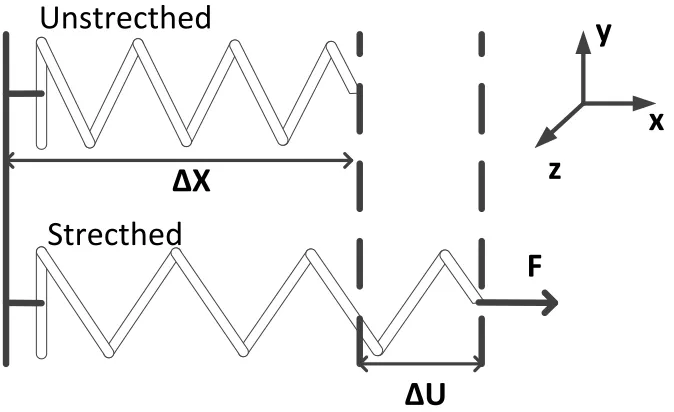
Figure 1.2 shows the deformation on a spring with an applied force. Δu is deformation or
F
Strecthed
Unstrecthed
ΔX
ΔU
x
y
z
Figure 1.2: Deformation of a spring with an applied force.
Strain is defined as:
𝜀𝑋𝑋 = 𝛥𝑢𝛥𝑥 (1.1)
Elastic materials return to its original shape when the force is removed.
Hooke’s law states the following relationship for stress and strain for the plane strain
condition [1.13]:
𝜎= 𝑐.𝜀 (1.2)
where σ and ε are stress and strain vectors, respectively (in the order of [𝑥𝑥,𝑦𝑦,𝑥𝑦]) and c is
the matrix of material constants given by Equation 1.3 for plane strain condition [1.13].
The plane strain condition refers to solids whose dimension in the z-direction is much greater
𝑐 =(1+𝑣)(1−2𝑣)𝐸(1−𝑣) ⎣ ⎢ ⎢ ⎢
⎡𝑣/(11− 𝑣) 𝑣/(11− 𝑣) 00
0 0 (1−2𝑣)�2(1− 𝑣) ⎦ ⎥ ⎥ ⎥ ⎤ (1.3)
This condition is widely used in our simulations in this study for the case of large transistor
widths; hence this constitutive equation is presented here for this reason.
In Equation 1.3, E and v are Young’s modulus and Poisson’s ratio.
Young’s modulus defines the stiffness of the material and the ratio of the uniaxial stress to
the uniaxial strain. Hence its unit is in Pascals. On the other hand, when a material is
compressed in one direction, it usually expands in other directions. Poisson’s ratio is defined
as this percent expansion to the percent compression for the small values of changes [1.13],
[1.14].
In the text, both σ and S will be used to denote stress. In addition, compressive stress will be
considered as negative and tensile stress as positive.
1.3 Basics of Finite Element Method (FEM)
In our study, detailed stress-strain calculations of CMOS stressors were performed by using a
finite element method (FEM) simulator, abaqus [1.15], which is suitable for calculating stress in arbitrary geometry [1.16]. In addition, it is convenient to apply changes in geometry
and simulation time is on the order of minutes, which makes FEM efficient to use in this
study.
partial differential equations for mechanics problem is constituted and then assembled
together to form the global finite element equation for the complete problem domain [1.13],
[1.17].
The solver traverses through all nodes in a mesh and creates the following equation for each
element.
[𝑘]𝑒{𝑢}𝑒 = {𝑓}𝑒 (1.4)
where [k]e is the element stiffness matrix, {u}e is the nodal displacement vector for the
element and {f}e is the element force vector [1.18].
Then the matrix equations for each element are assembled to create the global equation for
the problem.
[𝐾]{𝑢} = {𝑓} (1.5)
where K is the global stiffness matrix, u is the global displacement vector and f is the global
force vector [1.18].
Abaqus [1.15] generally uses Newton’s method in incremental time steps to solve static problems like Equation 1.5 [1.18].
1.4 Stress Sources in CMOS
Strained-Si was integrated to CMOS process in 2000s; however the idea can be traced back
to 1980’s. Both biaxial and uniaxial stress options were carefully analyzed and evaluated for
years, before the industry adopted uniaxial stress [1.19], due to continuous mobility
Figure 1.3 summarizes the desired stress types for hole and electron mobility enhancement.
Holes and electrons enjoy different type of stress on the channel direction and this introduces
extra process steps to the CMOS fabrication.
Figure 1.3: Desired Stress Types for CMOS Transistors.
Mechanical stress sources, used in state of the art CMOS technologies are summarized below
and visualized in Figure 1.4.
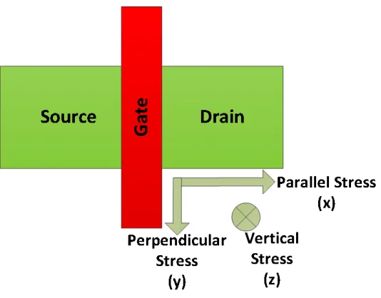
Figure 1.4: Mechanical Stress Sources in CMOS Transistors.
Direction PMOS NMOS Longitudinal (X) Compressive Tensile Lateral (Y) Tensile Tensile Out-of Plane (Z) Tensile Compressive
Parallel (x) Perpendicular (y) Vertical
Lattice-Mismatched Materials in Junction Regions: Si1-XGeX has a higher lattice constant
than Si, therefore exerts a high longitudinal compressive stress to the channel region of
PMOS transistors. This was first reported in [1.22] for the Intel’s 90nm logic technology.
The counterpart of embedded SiGe junction is embedded Si:C junction for NMOS devices
where the substitutional Carbon atoms are introduced to source/drain areas. Si:C has a
substantially lower lattice constant than Si, thus creates a tensile compressive stress along the
channel. However, integration of embedded Si:C junctions were found to be much more
challenging than embedded SiGe junctions, thus its use in commercial mass production is
still limited [1.23].
This stress source will be frequently referred as LMS throughout the paper.
Contact Etch Stop Liners (CESL): Contact Etch Stop nitride liners employ highly stressed Si3N4 films to exert stress through the active area and gate electrode. It was first integrated to
CMOS processes in 90nm technology [1.22], [1.24]. In [1.24] tensile liners for NMOS and
compressive liners for PMOS were employed, which is called as “Dual Stress Liners” (DSL).
Compressive and tensile etch stop liners are also used as cESL and tESL, respectively in this
paper.
Shallow Trench Isolation (STI): Unlike aforementioned stress sources, STI is a parasitic stress source. It is a result of thermal cycles during isolation process due to the differences in
thermal expansion coefficients of Si-SiO2 [1.25], [1.26]. It is compressive in nature.
Stress Memorization Technique (SMT): This technique improves electron mobility for NMOS devices without degrading PMOS performance. Unlike other stressors, the SiN layer
is a temporary layer which makes it relatively independent of layout [1.2]. Therefore SMT
will not be studied separately in this work.
Through Silicom Via (TSV): 3-D integration with through silicon vias (TSVs) offers an attractive alternative to 2-D planar technologies [1.50]. Similar to the STI stress, stress builds
up inside silicon during thermal cycles due to the thermal expansion coefficient difference
between TSV material and silicon [1.51].
1.5
Strained Silicon Physics
The carrier mobility is defined as [1.27]:
𝜇
=
𝑞.𝜏𝑚∗ (1.6)Where τ is the mean time between scattering events and m*
is the conductivity effective mass
of charge carriers.
Effective mass of the charge carriers can be calculated by [1.27]:
𝑚
∗=
𝑑2𝐸ħ𝑑𝑘2
� (1.7)
Where 𝑑
2𝐸
𝑑𝑘2 is the curvature of the (E, k) band.
Therefore, decreasing the effective mass by warping energy bands or increasing the mean
time between scattering events enhances the carrier mobility. Mechanical stress in silicon can
1.5.1 Hole Mobility Enhancement under Stress
In a PMOS device (on (001) Si plane and with [110] channel direction), compressive uniaxial
stress warps valance band in such a way that curvature of (E,k) band becomes larger [1.19],
[1.28]. Moreover, it breaks the symmetry of the light and heavy hole bands which results in
band mixing and redistribution of charge carrier, which decreases hole effective mass thus
increases its mobility [1.28], [1.29]. In addition to these two factors, as a result of warping,
available density of states decreases which result in a decrease of inter band scattering which
also contributes to mobility increase as much as 20% [1.28].
Similarly, biaxial stress also warps and shifts the bands and decreases effective hole mass but
significantly lower in magnitude than uniaxial stress [1.30]. In addition, biaxial stress
maintains symmetry of light and heavy hole bands unlike uniaxial strain [1.29].
The field dependences of uniaxial and biaxial stress are also different due to the different
physical effects they create on bands. Uniaxial stress is maintained in high vertical fields,
whereas biaxial stress loses its enhancement on mobility [1.29].
1.5.2 Electron Mobility Enhancement under Stress
Tensile uniaxial stress along the channel direction of an NMOS device (on (001) Si plane and
with [110] channel direction), warps energy surface and reduce the effective mass of
electrons, similar to holes under compressive uniaxial stress. Moreover, it also splits
conduction band edge and decreases inter-valley scattering, which also favors electron
mobility increase. On the other hand, tensile biaxial strain does not change effective mass of
an electron but increase mobility by just splitting conduction band edge. This difference
effects their behavior at high fields, since splitting of conduction band edge behavior is more
affected than effective mobility increase in large fields [1.31].
Furthermore, uniaxial stress does not saturate in high stress regime (up to 1.5GP) since
effective mass continues to decrease with the increasing stress. However inter-valley
scattering, which is the dominant effect in biaxial stress case, saturates in high stress regime
[1.31], [1.32].
1.6 Electrical Effects of Stress in CMOS
The most important outcome of strained silicon technology is mobility improvement. A
fractional change in mobility (𝛥𝜇 ⁄ 𝜇)is a linear function of stress (σ) and given by [1.33] :
Δμ/μ=�𝜋∥𝜎11 +𝜋⊥𝜎22+𝜋12𝜎33� (1.8)
where 𝜎11,𝜎22, and𝜎33 are the parallel, perpendicular and vertical stress to the channel.
(these components are also referred as SXX, SYY, and SZZ respectively in the later figures).
The π’s are the corresponding piezoresistance coefficients. The Piezoresistance effect is an
electrical resistance change with stress, which was discovered by Smith almost sixty years
ago [1.34]. Piezoresistance coefficient values depend on the direction of stress as well as
orientation of a wafer.
As Table 1.1 shows, hole and electron mobility improvement depend most on parallel and
vertical stresses, respectively [1.29], [1.33]. On the other hand, hole mobility is not affected
Table 1.1: Piezoresistance coefficients for <110> channel orientation on (001) wafer.
Coefficient PMOS (x10-11 Pa-1) NMOS (x10-11 Pa-1)
𝜋∥ (Parallel) 71.8 -31.6
𝜋⊥ (Perpendicular) -66.3 -17.6
𝜋12 (Vertical) -1.1 53.4
For hole mobility, at high values of 𝜎11 (more than 500MPa) which state of the art PMOS
transistors use, a fractional change in hole mobility does not show linear relationship with
stress. Hence the fractional increase due to the parallel stress cannot be calculated by using
piezoresistance coefficients. In [1.19], hole mobility enhancement 𝜇 𝜇⁄ 0 was extracted for a
wide range of stress values.
Figure 1.5 shows that mobility enhancement saturates around 4.5X-fold over relaxed Si. On
the other hand, electron mobility enhancement does not saturate in high stress regime (up to
1.5GP). Therefore the fractional change in electron mobility can be calculated with Equation
1.8.
Carrier mobility is mostly responsible for the linear region of operation and is not sufficient
to capture the behavior of transistors in saturation region [1.4]. Saturation velocity, on which
the effect of stress has been experimentally demonstrated [1.37], is mainly responsible for the
device behavior in the saturation region of operation. This impact is process dependent [1.4],
[1.37], and can be calibrated with data from a specific process to achieve better accuracy
𝛥𝐼𝐷𝑠𝑎𝑡
𝐼𝐷𝑠𝑎𝑡 = (1− 𝐵𝑠𝑎𝑡)
𝛥𝜇
𝜇 (1.9)
where Bsat is the saturation region ballistic coefficient which is around 0.6- 0.7 for the state of
the art technologies [1.36].
Figure 1.5: Mobility Enhancement (μ/μ0) vs. Parallel Stress σ11 (=SXX) for Uniaxial
compression in the direction of [110] on (001) Si wafer [1.19].
Therefore, saturation velocity BSIM4 parameter (vsat) is updated accordingly [1.37].
Mechanical stress also causes threshold voltage shift in NMOS transistors. The threshold
voltage change of an NMOS transistor under uniaxial tensile stress is given by [1.38], [1.39]:
𝑞.𝛥𝑉𝑇𝑁(𝜎) = (𝑚 −1)𝛥𝐸𝑔(𝜎) (1.10)
𝛥𝐸𝑔 = −6.19𝜀[110] eV (1.11)
𝜀[110] ≈ 𝜎𝑋𝑋⁄𝐸𝑆𝑖 (1.12)
ESiis Young’s Modulus of Silicon.
In [1.39] it was found that this model is consistent with measurement results. [1.40], [1.41],
[1.42] came to the conclusion that threshold voltage shifts are negligible (<5mV) for PMOS
transistors under stress. Therefore threshold voltage of PMOS transistors is assumed to be
independent of channel stress.
1.7 Previous Research in the Area of Stress Modeling
The influence of layout on stress sources has been studied by other researchers in the past.
Widely used BSIM4 model [1.37], only contains STI stress effect without taking STI length
into account, which has a considerable impact on STI stress. Researchers in [1.25], [1.26],
[1.42], [1.43] also limited their studies to STI impact on stress and did not model state-of the
art stress effects, which are more dominant in today’s technologies.
[1.44] presented analytical models for different sources of stress but limited their work for an
isolated transistor, which is not adequate to capture context dependent layout effects. In other
words, the model is unable to capture the variations between devices having same diffusion
length throughout the circuit layout. In addition, models do not include perpendicular (width
direction of a device) and vertical (gate direction of a device) directions of the stress tensor
which have non-negligible effects on device performance. Also, they did not model all
process dependent effects which make their model parameters process-dependent. Therefore,
the model is not readily available to use without calibrating for a specific technology, which
makes it impossible to use without having such data.
Researchers in [1.45], [1.46], [1.47] performed various TCAD simulations to capture
different process and layout dependent sensitivities on stress for a single device in an isolated
or dense environment. However, they mostly limit their studies on device level and did not
study context dependent effects. They created an analytical model for a single device with
lattice mismatch stressors in a dense environment; however due to lack of context dependent
effect, it would not be able to capture the variation between devices accurately. Furthermore,
they also pointed out the inaccuracy of their model for the absolute values of stress.
[1.4] created TCAD simulation-based physical models for different stress effects. However,
stress component in only one dimension (parallel to the channel) was modeled. In addition,
width dimension effects and contact holes, which contribute to stress variation significantly,
were not captured. Furthermore, process dependent parameters were left as constants, which
limit the model’s use for a designer.
[1.48] presented 1-dimensional string based equations for parallel and perpendicular
directional stress components, but due to the 1-D assumption, neighboring layout effects
were overestimated and the vertical component of stress was not modeled. Moreover, process
effects on stress were not captured which should be extracted for each specific process to be
used. Not having such data would limit the use of this model.
Even though [1.12] introduced process specific analytical models, details of the model are
[1.6], [1.49] indicated possible ways to mitigate device variations by using different layout
structures. However, their study is based on TCAD simulations without creating any
analytical model. In addition, their study does not include any process impacts.
The current trend in semiconductor industry is to model these effects with obfuscated,
proprietary models. However, the majority of these effects can be effectively captured in
public, non-process specific models capable of analyzing the systematic layout induced
mechanical stress variations.
1.8 Original Contributions
The main contribution of this dissertation is the development of process independent, context
dependent, open source, analytical stress models, which are interpolated based on over
22,000 finite element method simulations. There are separate analytical models for all
individual stress sources, lattice mismatch stressors (LMS), contact etch stop liners (CESL),
shallow trench isolation (STI) and through silicon via (TSV). Unlike other stressors, SMT is
a temporary layer which makes it relatively independent of layout [1.2]. Therefore SMT will
not be studied separately in this work.
The open source models capture all stress source effects in all directions with explicit
formulation of process dependence as well as layout dependence. In other words, models
accept process parameters as inputs which change both the magnitude of stress and its layout
sensitivity significantly.
The second contribution of this work is a Stress Advisor tool. It is a software tool
implemented using MATLAB® which can provide quick feedback to the layout designer about the effects of possible changes on layout before doing the actual layout changes which
can be cumbersome. A similar tool applied in [1.7] inspired this work, but it is for a specific
technology and it is not open source. The layout designer will input technology information
and then geometry information of a device and the tool returns the mobility multiplier and
threshold voltage changes. The designer quickly tries out different geometries according to
the desired performance of a device, and then does the layout changes accordingly. Figure
1.6 summarizes Stress Advisor flow.
By using the stress advisor flow, it is much easier to create restrictive design rules and layout
guidelines for a specific technology.
1.9 Organization
The dissertation is organized as follows: Chapter 2 presents a device level study of modeling
stress for lattice mismatch material in junction regions. Chapter 3 presents Contact etch stop
liner (CESL) stress modeling for isolated devices. In both chapters the detail analysis of
individual process effects are analyzed and their influence on layout sensitivity is discussed.
Chapter 4 presents study for shallow trench isolation (STI) stress. This work includes state of
the art enhancements for stress effect in shallow trench isolation processes. In Chapter 5, the
effect of neighboring layout features on the channel stress is studied. Chapter 6 studies
through silicon via (TSV) stress and presents compact model for it. In Chapter 7, analytical
model construction details along with the model validation against silicon measurements are
discussed. Chapter 8 concludes the dissertation by presenting possible future work
alternatives.
Throughout the paper, we compare our analytical model results against finite element
analysis results as well as experimental silicon measurement results. Hence in figures, the
labels “Model”, “Simulation”, and “Experimental” respectively will be used to distinguish
References
[1.1] G. E. Moore, “Cramming More Components Onto Integrated Circuits,” Electronics, Vol. 38, No.8, pp. 114-117, April, 1965.
[1.2] V. Joshi, B. Cline, D. Sylvester, D. Blaauw, and K. Agarwal, “Mechanical Stress Aware Optimization for Leakage Power Reduction,” IEEE Trans. on Computer-Aided Design of Integrated Circuits and Systems, vol.29, pp.722–736, May 2010.
[1.3] S. Flachowsky et al., “Detailed simulation study of embedded SiGe and Si:C source/drain stressors in nanoscaled silicon on insulator metal oxide semiconductor field effect transistors,” Journal of Vacuum Science & Technology B, vol. 28, March 2010.
[1.4] C.-C. Wang, W. Zhao, F. Liu, M. Chen, and Y. Cao, “Modeling of layout-dependent stress effect in CMOS design,” ICCAD '09, pp.513-520.
[1.5] S.E. Thompson et al., “A logic nanotechnology featuring strained-silicon,” IEEE Electron Device Lett., vol. 25, pp. 191-193, March 2004.
[1.6] V. Moroz, L. Smith, X.-W. Lin, D. Pramanik, and G. Rollins, “Stress-Aware Design Methodology,” ISQED '06, pp.807-812.
[1.7] A. Sultan et al., “CAD utilities to comprehend layout-dependent stress effects in 45 nm high- performance SOI custom macro design,” ISQED '09, pp.442-446.
[1.8] Z. Wei, F. Liu, K. Agarwal, D. Acharyya, S.R. Nassif, K.J. Nowka, Y. Cao, “Rigorous Extraction of Process Variations for 65-nm CMOS Design,” IEEE Trans. on Semiconductor Manufacturing, vol.22, no.1, pp.196-203, Feb. 2009.
[1.10] R.O. Topaloglu, “Characterization, Modeling and Optimization of Fills and Stress in Semiconductor Integrated Circuits” (PhD diss., University of California, San Diego, 2008).
[1.11] V. Joshi, “Variability Aware Analysis and Optimization of VLSI Circuits” (PhD diss., University of Michigan, 2011).
[1.12] E. Morifuji et al., “Layout Dependence Modeling for 45-nm CMOS With Stress-Enhanced Technique,” IEEE Trans. on Electron Devices, vol.56, pp.1991–1998, Sept. 2009.
[1.13] G.R. Liu, and S.S. Quek, “Finite Element Method A Practical Course”, Butterworth Heinemann, Feb. 2003.
[1.14] H. E. Randell, “Applications of Stress from Boron Doping and Other Challenges in Silicon Technology”, (Master of Science Thesis, University of Florida, 2005).
[1.15] Manual, Abaqus, Version6.8.
[1.16] Y.-C. Yeo, “Strain engineering for hole mobility enhancement in p-channel field-effect transistors,” Int. Conf. on Solid-State and Integrated Circuits Technology, pp. 310- 314, 2004.
[1.17] N. Shah, “Stress Modeling of Nanoscale MOSFET” (Master of Science Thesis, University of Florida, 2005).
[1.18] G.R. Liu, and S.S. Quek, “A finite element study of the stress and strain fields of InAs quantum dots embedded in GaA,” Semiconductor Science and Technology,
vol.17, pp.630-643, May 2002.
[1.20] K. Uchida, T. Krishnamohan, K.C. Saraswat, and Y.Nishi, “Physical mechanisms of electron mobility enhancement in uniaxial stressed MOSFETs and impact of uniaxial stress engineering in ballistic regime,” IEDM'05, pp.129-132.
[1.21] J.-S. Lim, S.E. Thompson, and J.G. Fossum, “Comparison of Threshold-Voltage Shifts for Uniaxial and Biaxial Tensile-Stressed n-MOSFETs,” IEEE Electron Device Lett. vol.25, pp.731-733, Nov. 2004.
[1.22] T. Ghani et al., “A 90nm High Volume Manufacturing Logic Technology Featuring 45nm Gate Length Strained Silicon CMOS Transistors,” IEDM'03, pp.11.6.1-11.6.3.
[1.23] B. Yang, et al., “High-performance nMOSFET with in-situ phosphorus-doped embedded Si:C (ISPD eSi:C) source-drain stressor,” IEDM '08, pp.1-4.
[1.24] H.S. Yang, et al., “Dual stress liner for high performance sub-45nm gate length SOI CMOS manufacturing,” IEDM '08, pp.1075-1077.
[1.25] R.A. Bianchi, G. Bouche, and O. Roux-dit-Buisson, “Accurate modeling of trench isolation induced mechanical stress effects on MOSFET electrical performance,”
IEDM '02, pp.117- 120.
[1.26] A.B. Kahng, P. Sharma, R.O. Topaloglu, “Exploiting STI stress for performance,”
ICCAD '09, pp.83-90.
[1.27] B.G. Streetman, and S.K. Banerjee, “Solid State Electronic Devices”, Prentice Hall, 2006.
[1.28] L. Shifren, et al., “Drive current enhancement in p-type metal–oxide–semiconductor field-effect transistors under shear uniaxial stress,” Applied Physics Letters, vol.85, no.25, pp.6188-6190, Dec. 2004.
[1.30] S.E. Thompson, et al., “A 90-nm logic technology featuring strained-silicon,” IEEE Trans. on Electron Devices, vol.51, no.11, pp. 1790-1797, Nov. 2004.
[1.31] K. Uchida, et al., “Physical mechanisms of electron mobility enhancement in uniaxial stressed MOSFETs and impact of uniaxial stress engineering in ballistic regime,”
IEDM '05, pp.129-132.
[1.32] A.T. Bradley, et al., “Piezoresistive characteristics of short-channel MOSFETs on (100) silicon,” IEEE Trans. on Electron Devices, vol.48, no.9, pp.2009-2015, Sept. 2001.
[1.33] A.T. Bradley, R.C. Jaeger, J.C. Suhling, and K.J. O’Connor, “Piezoresistive characteristics of short-channel MOSFETs on (100) silicon,” IEEE Trans. on Electron Devices, vol.48, pp. 2009–2015, Sept. 2001.
[1.34] C.S. Smith, “Piezoresistance Effect in Germanium and Silicon,” Physical Review, Vol.94, No.1, pp.42-49, April 1, 1954.
[1.35] M.S. Lundstrom, “On the mobility versus drain current relation for a nanoscale MOSFET, “ IEEE Electron Device Lett., vol.22, pp.293-295, June 2001.
[1.36] H.M. Nayfeh, “Channel strain engineering for high performance CMOS technology,”
IEEE Int. Conf. on Adv. Thermal Proc. of Semiconductors, pp. cxci-ccxviii, Sept. 2008.
[1.37] Manual, BSIM4, Version4.7.
[1.38] J.-S. Lim, S.E. Thompson, and J.G. Fossum, “Comparison of Threshold-Voltage Shifts for Uniaxial and Biaxial Tensile-Stressed n-MOSFETs,” IEEE Electron Device Lett. vol.25, pp.731-733, Nov. 2004.
[1.40] K. Wu, “Strain Effects on the Valance Band of Silicon: Piezoresistance In P-Type Silicon and Mobility Enhancement in Strained Silicon PMOSFET” (PhD diss., University of Florida, 2005).
[1.41] C. Gallon, G. Reimbold, G. Ghibaudo, R.A. Bianchi, and R. Gwoziecki, “Electrical analysis of external mechanical stress effects in short channel MOSFETs on (001) silicon,” Solid-State Electronics, vol.48, pp. 561-566, Apr. 2004.
[1.42] J. Xue, Z. Ye, Y. Deng, H. Wang, L. Yang, and Z. Yu, “Layout-dependent STI stress analysis and stress-aware RF/analog circuit design optimization,” ICCAD '09, pp.521-528.
[1.43] Jiying Xue; Yangdong Deng; Zuochang Ye; Hongrui Wang; Liu Yang; Zhiping Yu, “A Framework for Layout-Dependent STI Stress Analysis and Stress-Aware Circuit Optimization,” IEEE Trans. on Very Large Scale Integration (VLSI) Systems, vol.20, no.3, pp.498,511, March 2012.
[1.44] M.V. Dunga, X. Xi, A.M. Niknejad, and C. Hu, “A Holistic Model for Mobility Enhancement through Process-Induced Stress,” IEEE Conf. on Elect. Devices and Solid-State Circuits, 2005, pp.43-46.
[1.45] G. Eneman, E. Simoen, P. Verheyen, and K. De Meyer, “Gate Influence on the Layout Sensitivity of Si1-xGex S/D and of Si1-yCy S/D Transistors Including an
Analytical Model,” IEEE Trans. on Electron Devices, vol.55, pp.2703-2711, Oct. 2008.
[1.46] G. Eneman, P. Verheyen, A. De Keersgieter, M. Jurczak, and K. De Meyer, “Scalability of Stress Induced by Contact-Etch-Stop Layers: A Simulation Study,”
IEEE Trans. on Electron Devices, vol.54, pp.1446-1453, June 2007.
[1.47] G. Eneman, et al., “Scalability of Si1-xGex Source/Drain technology for the 45-nm
[1.48] V. Joshi, et al., “Closed-form modeling of layout-dependent mechanical stress,” DAC '10, pp.673-678.
[1.49] V. Moroz, et al, “The Impact of Layout on Stress-Enhanced Transistor Performance,”
International Conf. on Simulation of Semiconductor Processes and Devices, 2005,
pp.143-146, 01-03.
[1.50] W. Davis, J. Wilson, S. Mick, J. Xu, H. Hua, C. Mineo, A. Sule, M. Steer, and P. Franzon, “Demystifying 3D ICs: the pros and cons of going vertical,” IEEE Design & Test of Computers, vol.22, no.6, pp.498,510, Nov.-Dec. 2005.
[1.51] Li Yu, Wen-Yao Chang, Kewei Zuo, J. Wang, D. Yu, and D. Boning, “Methodology for analysis of TSV stress induced transistor variation and circuit performance,”
Chapter 2
Modeling Stress for Lattice Mismatch
Material in Junction Regions
2.1 Introduction
A MOSFET with embedded Si1-xGex source/drain junction technology was first proposed by
researchers from North Carolina State University [2.1]. This work showed that embedded
Si1-xGex source/drain junctions increase solid solubility of Boron and decrease the band gap,
both of which lead to decreased contact resistance.
However, the hole mobility enhancement of this method was first reported in [2.2] for Intel’s
parallel compressive stress to the channel region of PMOS transistors. They showed hole
mobility (μP) gains greater than %50 and saturation current (IDSATP) gains greater than %25
relative to unstrained silicon devices thanks to this technology.
The counterpart of embedded Si1-xGex junction is embedded Si1-yCy junction for NMOS
devices where substitutional Carbon atoms are introduced to source/drain junction areas. Si:C
has a substantially lower lattice constant than Si thus creates a tensile compressive stress
along the channel. Nevertheless, integration of embedded Si1-yCy junctions was found to be
much more challenging than embedded Si1-xGex junctions [2.3]. Although the first Si:C
transistor was built back in 2004 by [2.4], it is still not used in commercial mass production.
In 2008, IBM announced for the first time that they have more benefits from Si1-yCy
junctions over their standard baseline transistor in 45-nm technology [2.3].
In LMS technology, the stress-level in the transistor channel, and hence the mobility
enhancement of a device, depends heavily on process parameters as well as its physical
dimensions. This chapter presents these effects and the analytical modeling effort to capture
them.
This chapter is organized as follows. Section 2.2 and its sub sections discuss our technical
approach to the problem and finite element method (FEM) simulation details. In Section 2.3
and its sub sections, we present several results about process parameter impacts on stress and
layout sensitivity. In section 2.4, we present parameter ranges for our experiments and model
2.2 Technical Approach
The focus of this section is to use finite element method (FEM) to solve for stress-strain
fields in device channel exerted by embedded lattice mismatched junctions.
In FEM simulators, lattice mismatch stress is simulated in the framework of thermoelasticity.
The lattice mismatch is modeled by a corresponding thermal expansion coefficient between
the lattice mismatched stressor (LMS) and Si, and temperature was raised by 1K [2.5], [2.6].
The lattice mismatch strain between LMS and Si can be calculated by Equation 2.1, and
thermal strain can be found by Equation 2.2 [2.6].
𝜀0 = 𝑎𝑠𝑖𝑎−𝑎𝐿𝑀𝑆𝐿𝑀𝑆 (2.1)
where𝜀0is lattice mismatched strain, 𝑎𝑠𝑖 is the lattice parameter of silicon and 𝑎𝐿𝑀𝑆 is the
lattice parameter of LMS material; Si1-xGex or Si1-yC y.
𝜀𝑇= 𝑎𝑇𝛥𝑇=𝜀0 (2.2)
where 𝜀𝑇 is the thermal strain, 𝑎𝑇 is thermal expansion coefficient and 𝛥𝑇is the temperature
difference between initial and final states.
Therefore, required 𝑎𝑇 is found for the corresponding𝜀0 for 𝛥𝑇= 1𝐾.
The lattice constant of Si1-xGex can be calculated by Vegard’s Law [2.7] :
𝑎𝑆𝑖(1−𝑥)𝐺𝑒𝑥= (1− 𝑥)𝑎𝑆𝑖 +𝑥𝑎𝐺𝑒 (2.3)
Vegard’s Law is also valid for calculation of other mechanical properties of Si1-xGex used in
the simulation; such as Young’s Modulus and Poisson’s Ratio.
The smaller lattice constant of Boron, which is used as a dopant in p+ junctions, relieves
some part of compressive uniaxial strain induced by Si1-xGex film [2.1]. The lattice constant
of B doped Si1-xGex film can be calculated from equation 2.4 [2.8].
𝑎𝑆𝑖(1−𝑥−𝑦)𝐺𝑒𝑥𝐵𝑦 = (1− 𝑥 − 𝑦)𝑎𝑆𝑖+𝑥𝑎𝐺𝑒+𝑦𝑎𝐵 (2.4)
𝑦 ≈ 𝑁𝐵
(1−𝑥)𝑁𝑆𝑖+𝑥𝑁𝐺𝑒 (2.5)
where NB is dopant concentration of B and NSi (=5x1022cm-3) , NGe (=4.42x1022cm-3) are
atomic densities of Si and Ge, respectively.
Unlike Si1-xGex film, the lattice constant of Si1-yCy deviates from Vegards’s Law and is
given by [2.9]:
𝑎𝑆𝑖(1−𝑦)𝐶𝑦 = 𝑎𝑆𝑖 −2.4239𝑦+ 0.5705𝑦2 (2.6)
Since the Carbon concentration in Si1-yCy is small (y<3%) the elastic constants are assumed
to be equal to silicon’s.
Simulations used isotropic approximation for material properties. In addition, most of the
simulations used 2-D plane strain condition, which assumes large transistor widths. However
for width dependent effects, 3-D simulations were also employed. In [2.5], [2.6], it was found
that 2-D and 3-D simulations as well as isotropic approximation and anisotropy yield similar
results.
Furthermore, no defect generation and partial stress relaxation was allowed in LMS
simulations.
Table 2.1 and 2.2 presents lattice constants and mechanical properties of materials used in
Table 2.1: Lattice Constants of Materials.
Material Lattice Constant, 𝑎 (Å)
Si 5.431
Ge 5.646
C 3.567
B 3.806
Table 2.2: Material Properties at Room Temperature.
Material Young’s Modulus, E (GPa) Poisson’s Ratio, v
Si 162.91 0.28
Ge 131.66 0.273
Polysilicon 169 0.22
SiO2 70 0.17
Silicon Nitride 192 0.24
TiN HfO2 600 280 0.25 0.2
2.2.1 FEM Modeling of an Isolated Transistor
A simplified isolated transistor structure used in the 2-D stress-strain simulations of junctions
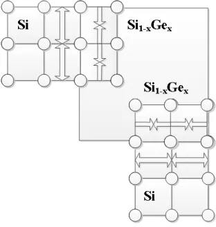
with embedded lattice mismatch stressor is shown in Figure 2.1. Table 2.3 explains the
Figure 2.1: Transistor structure with Lattice Mismatched Stressor for FEM simulation.
Table 2.3: Parameter Explanations for Figure 2.1.
Parameter Name Parameter Type Explanation
LS/D Layout Parameter Active Area or diffusion length
LSTI Layout Parameter STI length nearby the device
LLMS Process Parameter Spacing between source and drain stressors
ΔLMS Process Parameter Spacing between LMS and device channel
dLMS Process Parameter Recess depth of the LMS
hLMS LGATE hGATE Process Parameter Process Parameter Process Parameter
Fill height of the LMS above the Si-Gate
Oxide interface
Gate Length. 𝐿𝐺𝐴𝑇𝐸= 𝐿𝐿𝑀𝑆−2.𝛥𝐿𝑀𝑆
Gate height
LSPACER Process Parameter Spacer width of the device
U-shaped LMS Process Parameter Physical shape of the LMS
Σ-shaped LMS Process Parameter Physical shape of the LMS
GOX Process Parameter Gate Oxide of the device
In addition, device width, which in y-direction in Figure 2.1, also has an effect on channel
stress which cannot be captured from 2-D simulations. Therefore, the device structure in
Furthermore, there are other process parameter which are not geometrical but affecting the
layout sensitivity of channel stress which will be analyzed in upcoming sections.
2.2.1.1 Modeling LMS-Si Interface
Both LMS materials, Si1-xGex and Si1-yCy, are grown on etched recessed S/D junction areas
by epitaxial growth [2.12]. To get maximum benefits from stressors, epitaxial growth should
not have any misfit dislocations [2.13]. In other words, the growth should be pseudomorphic,
where both materials get strained without having dislocation defects [2.7]. The
Pseudomorphic growth is visualized in Figure 2.2.
Figure 2.2: Si - Si1-xGex Interface.
2.2.1.2 Mesh and Boundary Conditions
In FEM simulations, nonuniform mesh grid sizes, which are as small as 0.33 nm in the region
of high stress gradient, are employed. For 2-D simulations, 4-node bilinear quadrilateral
plane strain and for 3-D simulations, 8-nodal tri-linear hexahedral solid elements were used
[2.14].
Bottom of the shape shown in Figure 2.1 is constrained in every direction and right side is
constrained in x-direction, which means there is no horizontal displacement. The left side has
a symmetry boundary condition as shown in the Figure 2.1. No other loads, other than
aforementioned temperature rise, are applied to the free surfaces [2.5], [2.6].
2.3 Simulation and Modeling Results of Layout Sensitivity in an Isolated
Transistor
In this section, simulation and modeling results of layout sensitivity in an isolated transistor
will be presented under different process conditions. Transistor active area is bounded by the
shallow trench isolation as visualized in Figure 2.1. The directions of stress, which will be
Figure 2.3: Directions of Stress.
Lattice mismatched stressor (LMS) types and resulting stresses in all directions (for wide
transistors) are given in Table 2.4.
Table 2.4: LMS types and resulting Stress Types for all directions.
Stress Direction Si1-xGex Stress Direction Si1-yCy
Parallel Compressive Parallel Tensile
Perpendicular Compressive Perpendicular Tensile
Although simulations and modeling are achieved for both Si1-xGex and Si1-yCy, stress
sensitivity for different process and layout parameters will mostly be presented for Si1-xGex
since the results are valid for both stressor types, except the sign of the stress.
Perpendicular Stress (SYY) and Vertical Stress (SZZ) are generally less than 30% of the
Parallel Stress (SXX) in absolute value but simulation and modeling results for stress values
in all three directions will be presented throughout the chapter for completeness and
accuracy. However, parallel stress is the main focus of the study.
Stress varies along the transistor channel and the most critical position for carrier mobility
improvement is non-trivial; therefore, the stress is averaged along the transistor channel 2nm
under the gate oxide in this study [2.5], [2.17].
Stress is higher in Si-LMS interface and gradually decreases towards the channel center.
Stress variation is the largest for the longest stressor spacing (for Figure 2.4, LMS= Si1-xGex)
and it gradually decreases as channel length gets shorter. For LLMS=150nm, variation is
around 4X and it drops to 1.4X for LLMS=14nm.
Below, different process conditions and their effect on layout sensitivity will be discussed.
Layout sensitivity for an isolated transistor will be analyzed as follows.
i) By varying the active area length (LS/D): Larger active area means more stressor
material nearby the channel hence more stress. In addition, LS/D changes the
distance of STI to the channel, hence increasing LS/D will reduce STI effect on
ii) By varying the STI length (LSTI): SiO2 is a softer material than Si and it relaxes the
stress transferred to the transistor channel generated by the LMS material [2.17],
[2.18]. Longer STI length creates more stress relaxation and hence lower channel
stress.
Figure 2.4: Parallel Stress Distribution along Transistor Channel for different Si1-xGex
Figure 2.5: Simulated and Modeled Parallel Stress vs. Diffusion Length (LS/D) for different
STI Lengths (LSTI). (For simulations: LLMS=50nm, dLMS=100nm, hLMS=0nm, hGATE=100nm,
LSPACER=20nm, ΔLMS=10nm. Wide transistors with poly gate, nitride spacers and U-shaped
junctions with 25% Ge and 0 Boron concentrations.)
Figure 2.6: Simulated and Modeled Parallel Stress vs. STI Length (LSTI) for different
Diffusion Lengths (LS/D). (For simulations: LLMS=50nm, dLMS=30nm, hLMS=0nm,
hGATE=100nm, LSPACER=20nm, ΔLMS=10nm. Wide transistors with poly gate, nitride
![Figure 1.5: Mobility Enhancement (μ/μ0) vs. Parallel Stress σ11 (=SXX) for Uniaxial compression in the direction of [110] on (001) Si wafer [1.19]](https://thumb-us.123doks.com/thumbv2/123dok_us/1583081.1194980/30.612.182.454.190.405/figure-mobility-enhancement-parallel-stress-uniaxial-compression-direction.webp)