University of South Carolina
Scholar Commons
Theses and Dissertations
2017
Study of Mos2 and Graphene-Based
Heterojunctions for Electronic and Sensing
Applications
Ifat Jahangir
University of South Carolina
Follow this and additional works at:https://scholarcommons.sc.edu/etd Part of theElectrical and Computer Engineering Commons
This Open Access Dissertation is brought to you by Scholar Commons. It has been accepted for inclusion in Theses and Dissertations by an authorized administrator of Scholar Commons. For more information, please [email protected].
Recommended Citation
Study of MoS
2and graphene-based heterojunctions for
electronic and sensing applications
byIfat Jahangir
Bachelor of Science
Bangladesh University of Engineering and Technology, 2011
Master of Science
University of South Carolina, 2015
Submitted in Partial Fulfillment of the Requirements
For the Degree of Doctor of Philosophy in
Electrical Engineering
College of Engineering and Computing
University of South Carolina
2017
Accepted by:
MVS Chandrashekhar, Major Professor
Mohammod Ali, Committee Member
Guoan Wang, Committee Member
Goutam Koley, Committee Member
Dedication
Acknowledgements
I would like to thank my Supervisor Dr. MVS Chandrashekhar for supporting me
during these three years. Working with Dr. Chandra, in my opinion, is the best thing that
a Ph.D student can wish for. He perfectly translates the character of his students and
provides the best conditions for the development of intellectual qualities and creative
thinking. I am very grateful to him for his scientific advice and knowledge and many
insightful discussions and suggestions he provided me and beyond all his guidance in my
tough times.
I owe my gratitude to Dr. Goutam Koley, my MS advisor, a great mentor,
collaborator and also a member of my dissertation defense committee, for his guidance
and constant support during the last five years. Many of the works I have done during my
MS and Ph.D would not be possible without his support.
Then I would like to thank Dr. Mohammod Ali and Dr. Guoan Wang, members of
my dissertation defense committee, for their valuable suggestions and guidelines, which
not only made me think about my research from diffeent perspectives, but also enabled
me to showcase my work more effectively.
I would like to acknowledge the financial support from NSF grants that funded
my research during these years. I thank to all the present members of Dr. Chandra’s and
Dr. Koley’s groups. I would like to specially thank Anusha Balachandran, Surya Chava,
I wish to express my heartfelt gratitude to my family – my parents and my brother,
for always having faith in me and for bringing me this far. I would also like to thank all
my friends who were very supportive during the entire duration of my stay here in
Columbia, South Carolina. Finally and most importantly, I would like to express my deep
gratitude towoards the Almighty for giving me the ability to finish this work smoothly, I
Abstract
Since the discovery of graphene, there has been an increase in two-dimensional
(2D) materials research for their scalability down to atomic dimensions. Among the
analogs of graphene, transition metal dichalcogenides (TMDs) are attractive due to their
exceptional electronic and optoelectronic properties. MoS2, a TMD, has several
advantages over graphene and the industry workhorse Si, and has been reported to
demonstrate excellent transistor performances. The key obstacle in the commercialization
of MoS2 technology is low carrier mobility over large areas for top-down devices.
Although there were several early reports on synthesis of atomically thin MoS2 with
moderate mobility, transferring large area grown films to a substrate of choice leads to
interface charges that degrade mobility. In our work, a top-down growth technique for
synthesizing large area, 3-5 monolayers (ML) thick MoS2 film have been presented by
pre-oxidation of metallic Mo instead of direct sulfidation. The growth temperature was
significantly reduced in this method, eliminating free sulfur-induced degradation of the
SiO2 gate dielectric. As a result, the leakage current was suppressed by a factor of >108,
when compared to a single step direct sulfidation method. Using these thin films,
back-gated field effect transistors have been demonstrated with accumulation electron
mobility >80 cm2/Vs, on/off >105, and subthreshold swing of 84 mV/dec; which are among the best results for MoS2 based transistors on SiO2 substrate. A hypothesis on
The second part of our work aims at utilizing the best properties both graphene
and MoS2 simultaneously by forming a heterojunction of these two atomically thin
materials. Interestingly, these two materials have certain contrasting properties, for
example, graphene based FETs have poor switching performance while MoS2 based
FETs can outperform many state-of-the-art ultra-low power transistors. Fabricating a
Schottky diode made of graphene and MoS2 allows the unique properties of these two
materials to be combined and has been shown to be useful. A key property of these 2D
heterojunctions is that each constituent of the heterojunction is so thin that it may not be
able to completely screen an electric field from the second constituent, i.e. the Debye
screening length can be greater than the layer thicknesses, so that voltage-induced
interfacial tuning is achievable. This capability is unique to thin layers, most practically
achieved in 2D heterojunctions, and has been exploited in recent “barristors”, which are
3-terminal devices with Schottky diodes where the barrier height can be tuned by an
insulated gate. Such a tunable Schottky diode, similar to a triode vacuum tube is
attractive for applications in RF circuits, photodetection and chemical sensing, analog
and digital electronics, etc, with all the advantages of solid state devices e.g. high speed,
low-cost and compactness. In this work, a graphene/MoS2 heterojunction on SiO2
dielectric has been fabricated to demonstrate a functional barristor device. By varying the
gate bias between -20 V and +10 V, the barrier height could be modulated by >0.65 eV,
potentially enabling current control over 10 orders of magnitude at room temperature.
Using the current-voltage (I-V) and capacitance-voltage (C-V) characteristics of this
device, we have also extracted the Richardson’s coefficient and electronic effective mass
required for proper engineering of these devices. After that, various applications of the
barristor device have also been explored. The high optical response of the barristor has
demonstrated the presence of photoconductive gain, and has been consistent with the
changes in Schottky barrier height caused by the back-gate. The barristor has also been
successful as gate-tunable toxic gas sensors, with lowest level detection lying around 100
ppb (parts per billion) for NO2 and 1 ppm (parts per million) for NH3. These observations
highlight the potential applications of the graphene/MoS2 barristor for various electronic,
optoelectronic and sensing applications.
Finally, a mixed dimensional barristor made of graphene/InN nanowire
heterojunction with a backgate has been demonstrated. The surface passivation of InN
and the tunnel barrier formation at the graphene/NW interface have been achieved
through controlled O2 plasma exposure, which has allowed an otherwise ohmic contact to
turn into a gate tunable Schottky junction with >1 eV barrier height. This device has
been demostrated to perform sub-ppb level trace gas detection, photo-detection with very
high sensitivity and a novel gate-controllable memristive action through longer O2
Table of Contents
Dedication ... iii
Acknowledgements ... iv
Abstract ... vi
List of Figures ... xii
List of Tables ... xxi
Introduction... 1
Chapter 1 1.1 Overview ... 1
1.2 Synthesis of MoS2 and other 2D Materials ... 5
1.3 Electronic Properties and Applications of the TMDs ... 7
1.4 2D Materials in Optoelectronics ... 16
1.5 2D Materials Used for Sensing ... 20
1.6 Dissertation Outline ... 22
References ... 23
Synthesis and Characterization of MoS2 thin Films ... 34
Chapter 2 2.1 Synthesis of MoS2 via pre-oxidation ... 34
2.2 Characterization of MoS2 FET ... 40
Graphene and MoS2 based Heterojunctions ... 59
Chapter 3 3.1 Applications of graphene/semiconductor Schottky diodes: Review ... 60
3.2 Applications of Graphene-based Barristors: Review ... 73
3.3 Graphene/MoS2 Heterojunction Diodes: Review ... 75
References ... 81
Graphene/MoS2 Barristor: Electronic and Optical Characteristics ... 89
Chapter 4 4.1 Growth and Fabrication of the Barristor Devices ... 90
4.2 Electrical Characteristics ... 93
4.3 Band Diagram of the Barristor Device ... 102
4.4 Optical Response ... 105
References ... 109
Graphene/MoS2 Barristor: Sensing Experiments and Results ... 113
Chapter 5 5.1 Types of Sensors ... 113
5.2 Sensing Setup ... 119
5.3 Conductance-based Sensing Experiments ... 120
5.4 Capacitance-based Sensing Experiments ... 125
References ... 127
Graphene/InN Nanowire Based Mixed Dimensional Barristor ... 129
Chapter 6 6.1 Growth and Characterization of InN Nanowires ... 130
6.3 Characterization of Graphene/InN NW Heterojunction ... 138
6.4 Detection of Trace Gases Using Graphene/InN NW Barristor ... 144
6.5 Highly Sensitive Barristor Based Photo Detector ... 151
6.6 Gate Tunable Memristor ... 158
References ... 161
Conclusion ... 164
Chapter 7 7.1 Summary ... 164
7.2 Suggested Future Works ... 165
List of Figures
Figure 1.1: (a) Three-dimensional schematic representation of a typical MX2 structure,
with the chalcogen atoms (X) in yellow and the metal atoms (M) in grey.[18] (b) Schematics of the structural polytypes: 2H (hexagonal symmetry), 3R (rhombohedral symmetry, trigonal prismatic coordination) and 1T (tetragonal symmetry, octahedral coordination).[19]... 2 Figure 1.2: (a) Schematic of CVD of MoS2 from solid S and MoO3 precursors (left) and
resulting MoS2 films on SiO2 (right)[54]. The red dots indicate the heating elements in the
furnace. In this optical microscopy image, the lighter regions are MoS2 and the darker
regions are SiO2. (b) CVD growth of MoS2 from a solid layer of Mo on SiO2 exposed to
S vapour (top left), resulting in MoS2 layers that are visible in optical microscopy
(right)[55]. Bottom left: side-view schematic of an MoS2 layer on the Si/SiO2 substrate. (c)
CVD growth of MoS2 from a dip-coated precursor on the substrate and growth in the
presence of Ar gas and S vapour[56]. ... 5 Figure 1.3: Band structures calculated from first-principles density functional theory (DFT) for bulk (left) and monolayer (right) MoS2. ... 8
Figure 1.4:Schematic illustration of HfO2-top-gated monolayer MoS2 FET device [38]. . 10
Figure 1.5: Source–drain current (Ids) versus top gate voltage (Vtg) curve recorded from
the top-gated device in Figure 5.1 for a bias voltage ranging from 10 mV to 500 mV[38]. Measurements are performed at room temperature with the back gate grounded. Top gate width, 4 mm; top gate length, 500 nm. The device can be completely turned off by changing the top gate bias from −2 to −4 V. For Vds = 10 mV, the Ion/Ioff ratio is >1 × 10⁶.
For Vds = 500 mV, the Ion/Ioff ratio is >1 × 10⁸ in the measured range while the
subthreshold swing S = 74 mV dec−1. ... 11 Figure 1.6: (Left) Integrated circuit based on single-layer MoS2[84]. (Right) Schematic of
electric double-layer transistor (EDLT, a FET gated by ionic liquids)[86]. VDS is the
source–drain voltage and VG is the gate voltage. ... 12
Figure 1.7: Conductivity as a function of top gate voltage for both bulk and thin-flake MoS2 EDLT devices[86]. Thin-flake devices show on/off ratios >102 for both electron and
hole transport. ... 13
Figure 1.8:Simulated device characteristics for a monolayer MoS2 FET device with
2.8-nm-thick HfO2 top-gate oxide, 15-nm gate length, and power supply voltage 0.5 V[98].
Figure 1.9: Proposed TMDC-based high-electron-mobility transistor (HEMT) device with top-gated Schottky contact and TMDC layers with different doping levels[20]. ... 15 Figure 1.10:Atomic force microscopy image of MoS2 monolayer flake (left) and optical
microscopy image of this flake made into a device with metal contacts (right). The white trace in the left panel shows a height profile from AFM along the MoS2 flake edge[114]. 16
Figure 1.11: Photoswitching characteristics of single-layer MoS2 phototransistor at
different optical power (Plight) and drain voltage (Vds)[114]. ... 17
Figure 1.12: Photoswitching rate (left) and stability test (right) of photoswitching behaviour of single-layer MoS2 phototransistor at Vds = 1 V, Plight = 80 μW[114]. ... 18
Figure 1.13: Energy-level diagram of proposed multijunction solar cell made of stacked semiconductors of different bandgaps to absorb different wavelengths from the solar spectrum to reduce thermalization losses. The blue dashed lines represent the quasi-Fermi levels defining the open-circuit voltage, and yellow dots represent electrons in the device[109]. ... 19 Figure 1.14: Proposed solar-cell device with parallel structures that may be fabricated using lift-off and printing techniques for patterning the semiconductor layers and a micro- or nanophotonic spectrum-splitting layer. The various bandgaps available from the different TMDCs are promising for use in such multijunction photovoltaic devices[20]. . 20 Figure 2.1: Tube furnace, temperature and mass flow controller systems used for MoS2
synthesis. ... 35
Figure 2.2: Temperature, pressure and gas flow rates during various stages of the growth of MoS2. The Y-axis is not to scale and the plots are shifted vertically for clear
understanding. ... 36
Figure 2.3: Raman spectra of oxidized pre-growth Mo samples showing peaks for various oxides of Mo.[7] ... 37 Figure 2.4: Raman spectra of MoS2 with E12g peak at 383 cm-1 and A1g peak at 406 cm-1;
the separation of the peaks is 23 cm-1, which is generally observed in 3-5 ML MoS2.[5] All
the peaks from MoOx are undetectable after sulfidation, indicating a total conversion of
all such oxides. ... 38
Figure 2.5: Tapping mode atomic force microscopy image of MoS2 on SiO2 (inset) with a
step height of 1.7 nm along the edge of the MoS2 film, corresponding to ~3ML, in
agreement with the Raman results. ... 39
Figure 2.6: Magnitude of gate leakage current through the SiO2 layer at VDS = 0.5 V,
using current three-step recipe and an alternative recipe with one-step direct sulfidation at high temperature. The insulating property of SiO2 is severely compromised during direct
Figure 2.7: Schematic of the device, showing the electrical test configuration and the pinching-off of the channel by the depletion region at VDS > VDS,sat... 41
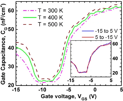
Figure 2.8: Gate capacitance-voltage (C-V) characteristics of a MoS2 FET showing
charge accumulation, depletion and inversion with different gate voltage biases and temperatures. The inset shows C-V curves using alternating sweep directions without any sign of hysteresis. ... 42
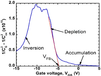
Figure 2.9: Estimation of flat band voltage (VFB) using the 1/C2 vs VGS curve near the
knee point of the depletion region. ... 43
Figure 2.10: Energy band diagrams of the MoS2-based MOS capacitor structure at
different bias ranges. (a) At thermal equilibrium, electrons are pulled near the MoS2/SiO2
interface by the electric field established by the interface charges and the work function difference between Si and MoS2. (b) At VGS > 0 V, more electrons accumulate. (c) The
opposite event takes place at depletion (e.g. VGS = VFB < 0 V) regime where electrons are
repelled and holes are attracted, thus flattening the band. (d) At VGS < VFB inversion
regime takes place, where the energy bands bend to such extent that the material acts like a p-type semiconductor and accumulates holes. ... 44
Figure 2.11: Transfer characteristics of MoS2 based FET with W=20 μm, L = 100 μm and
VDS = 0.5 V, showing drain current as a function of gate voltage
at different temperatures. ... 45
Figure 2.12: The linear ID vs VGS curves for the same data as shown in Figure 2.11,
showing the threshold voltage, VT’s, determined by the X-axis intercept of the
dashed tangent lines . ... 46
Figure 2.13: Transconductance curves at different drain bias voltages (VDS) between
0.5 V and 2.5 V. ... 47
Figure 2.14: Transfer curves at VDS = 2.5 V measured with the gate bias swept from -15V
to 5 V and 5 V to -15 V. The identical transfer curves in both sweep directions indicate the absence of hysteresis. ... 47
Figure 2.15: Transfer characteristics with drain voltages from 0.5 V to 2.5 V to show the effect of VDS at T=300K. ... 48
Figure 2.16: Normalized T=300K ID-VDS characteristics of the back-gated MOS2 FET
with respect to gate voltage VGS, shown in two distinct regimes. The first one ranges from
-8 to 4 V with electrons being the majority carriers. The second regime (dashed curves, VGS = -13 ~ -15 V) shows highly non-linear trends in the inversion regime with holes
being the majority carriers. ... 49
Figure 2.18: Variation of Rc as a function gate bias, measured using transmission line
measurements. ... 51
Figure 2.19: Field effect mobility (μFET) and sheet carrier concentration (ns) as a function
of VGS, with inset showing the weak temperature-dependence of electron μFET. ... 52
Figure 2.20: (a) Energy band diagram of the MoS2 FET at low VDS. At VGS>>VT,
thermionic emission (1) is the dominant mechanism of electron injection in the channel, which is facilitated by the low metal-semiconductor barriers at both ends of the channel by the accumulation of electrons in the channel. (b) At VGS << VT, there are several
possible mechanisms for hole transport in the valence band: (1) thermionic emission, (2) intra-band hole tunneling at both ends of the channel and (3) band-to-band tunneling at the drain end. ... 53
Figure 3.1: Schematic of the monolayer G/Si junction device of Ref. [14]. (b) I–VI–V curves of the device under darkness and weak illumination (P=1.23μW, λ=488nm) showing a conventional photodiode-like behavior. (c) Deviation of the I–V curves from a conventional photodiode response as the incident light power is increased up to P=6.5mW (the red dashed line corresponds to the expected behavior of a conventional M/S diode). (d) Thermal equilibrium energy band diagram in darkness (the Fermi level of n-Si is pinned to the charge neutrality level of its own surface states and ΦB≈0.8eV).
Band diagrams and Fermi level EF in darkness (dashed line), and quasi-Fermi level at
high irradiation power under (e) forward and (f) reverse bias (the subscript S is used for silicon)... 63
Figure 3.2: Spectral responsivity of the device (shown in the inset) of Ref. [14,17] in (a) high-gain mode and (b) photodiode mode. A dramatic difference in their magnitudes is observed, even though the spectral shapes are similar. (c)–(e) Schematics outlining the gain mechanism at the G/Si junction. Electrons and holes are denoted by dark and light circles, respectively. In (c) the dark current Idark is due to intrinsic carriers in graphene. (d)
Incident photons generate e–h pairs in the (lightly n-doped) silicon. Holes are swept into graphene by the built-in electric field of the junction and contribute to the current in the external circuit. Due to the fast transit time of graphene and the low probability of back injection in silicon, a single injected photocarrier can circulate several times (e) and substantially contribute to the current before recombine (f). This mechanism generate an internal quantum gain. ... 64
Figure 3.3: Solar cell with films of graphene on n-Si[37]. (a) Layout and a photograph of the devices. (b) Energy diagram of forward-biased G/n-Si Schottky junction upon illumination (c) I–VI–V characteristics of two devices (0.1 cm2 and 0.5 cm2) showing excellent rectification. The insets show the ideality factor and the series resistance of the 0.1 cm2 cell extrapolated from the forward linear region (d) Solar cell parameters (JSC,
VOC, FF and PCE) vs. light intensity for the 0.1 cm2 G/n-Si cell... 69
Figure 3.4: Solar cell with films of graphene on n-Si[37]. (a) J–V curves of cells
Figure 3.5: (a) Device schematic and biasing of a graphene chemiresistor and a G/Si Schottky diode sensor fabricated on the same chip[40]. (b) I–V characteristics of a G/p-Si (the positive voltage bias is applied to the Si contact). (c–d) Reverse I–V characteristics of G/p-Si diode in dark (solid curve) and under illumination (dotted curve) for different exposure times to (c) NO2 and (d) NH3. The black curves represent pre-exposure
characteristics, while the red and blue curves represent characteristics after 10 min and 30 min of gas exposure. ... 71
Figure 3.6: Layout of a graphene barristor with top gate[42]. (b) I–V characteristic of graphene/p-Si barristor at VGS = 0 V. (c) I–V characteristics of the pp-type barristor for
biases in the range −1.5 V to 1.5 V and gate in the range (−5,5) V by steps of 2 V. (d) SBH and field-effect induced Fermi level change, ΔEF. (e–f) Band diagram of
graphene/n-Si barristor (from left to right: gate–insulator–graphene–silicon) for (e) negative voltage on the gate (Vgate<0V and holes induced in graphene), and (f) positive
voltage on the gate (Vgate>0V and electrons induced in graphene). ... 74
Figure 3.7:Energy band alignment at the graphene/MoS2 interface on MoS2 single crystal
as derived from photoemission studies[53]... 77 Figure 3.8:(a) Schematic of a G/MoS2 back-gated FET (typical channel length and width
are 12 μm and 20 μm)[54]. Graphene is used as source/drain contact while MoS2 is the
FET channel. (b) Source–drain current at 0.5V source–drain bias as function of the back-gate voltage Vg. (c) Richardson plot ln(Id/T3/2) vs. 1000/T at different Vg. (d) Schottky
barrier height as a function of the back gate bias for the G/MoS2 and Ti/MoS2
heterojunctions. (e) Schematic band diagram of G/MoS2 heterostructure at Vg = 0 V and
Vg > 0 V. ... 78
Figure 3.9:(a) Schematic of a gate controlled G/MoS2 heterojunction[55]. The Si substrate
is the back-gate, while the channel includes a G/MoS2 heterojunction. Source and drain,
respectively connected to graphene and MoS2, are contacted by evaporated Cr/Au leads.
(b) Optical image of the device in (a). The MoS2 and graphene are ∼8 nm and ∼3 nm
thick, the overlapping area of graphene and MoS2 is about 1 μm2. (c) Source–drain
current vs. source drain bias (Id−Vd) at Vg = 0 V showing rectifying behavior due to the
Schottky barrier formed at the G/MoS2 interface. (d) Output characteristics Id−Vd at
different gate biases. (e) SBH as a function of Vg at drain bias Vd = 0 V: a sweep of the
gate voltage from −40 V to +40 V results in a variation of 0.34 eV of the SBH (or of the Fermi level of graphene). (f) Transfer characteristic of the G/MoS2 FET of (a). ... 80
Figure 4.1: Schematic of the simultaneously fabricated MoS2 FET, MoS2/graphene
heterojunction device and graphene FET on the same SiO2/n+ Si substrate. ... 91
Figure 4.2: Optical microscopy image of the fabricated device showing the partially overlapping MoS2 and graphene films with their metal contacts. ... 92
Figure 4.3: Raman spectra of graphene and (inset) MoS2. The D, G, 2D peaks of
Figure 4.4: Individual transfer characteristics of the MoS2 and graphene based FETs at
0.1 V drain bias. ... 93
Figure 4.5: I-V characteristics of the MoS2/graphene heterojunction at ~180 K temperature, with ideality factor of 1.12 and reverse saturation current of about 200 fA. 94 Figure 4.6: I-V curves for three different back-gate biases for the MoS2/graphene barristor device at ~180 K (dark), with the drain contact being on graphene... 95
Figure 4.7: Arrhenius plots of J0/T2 as a function of 1/T for different back-gate biases, used for calculating effective Schottky barrier height and Richardson’s coefficient for each case using thermionic emission model. ... 98
Figure 4.8: 1/C2 vs reverse bias for MoS2/graphene barristor at room temperature for three different back-gate biases, with and without illumination. ... 99
Figure 4.9: Calculated dark current at VDS = -1 V and barrier heights from C-V and I-V measurements of MoS2 without illumination for different back-gate biases. ... 99
Figure 4.10: Calculated barrier heights from (top) I-V and (bottom) C-V measurements respectively, as a function of VBG and presence/absence of light (10 W/m2 optical power). ... 100
Figure 4.11: Carrier concentration (n) variation obtained from the C-V measurements in Figure 4.10. ... 101
Figure 4.12: Band diagram of the barristor device in thermal equilibrium (VDS = 0 V), showing the Schottky barrier height (φ) for (a) positive and (b) negative gate biases. The charge balance diagrams are shown below each band diagram. ... 103
Figure 4.13: Photo response of the barristor device at different gate and drain bias voltages. ... 104
Figure 4.14: Transfer curve of the barristor at VDS = -1 V in the dark, which is used to calculate the estimated photo response by taking the photo-induced barrier height lowering. The measured photo response closely matches with it. ... 105
Figure 4.15: Photocurrent at 10 W/m2 optical power, measured for different grate and drain biases... 106
Figure 4.16: Effect of temperature on the photocurrent at fixed bias conditions. ... 107
Figure 5.1 Various applications of chemical sensors... 118
Figure 5.2: VOC sensing setup. ... 119
Figure 5.4: Percentage change in conductance of Graphene/MoS2 heterojunction FET on
100 nm SiO2/Si to 800 ppb of NO2 at various gate biases and for VDS = -1 V (dark). ... 122
Figure 5.5: Percentage change in conductance of Graphene/MoS2 heterojunction FET on
100 nm SiO2/Si to various concentrations of NO2 at VBG = -3 V, VDS = -1 V (dark). ... 123
Figure 5.6: Percentage change in conductance of graphene FET, MoS2 FET and
Graphene/MoS2 heterojunction FET on 100 nm SiO2/Si to various
concentrations of NH3. ... 124
Figure 5.7: Percentage change in conductance of Graphene/MoS2 heterojunction FET on
100 nm SiO2/Si to 5 ppm of NH3 at various gate biases and for VDS = -1 V. ... 124
Figure 5.8: Percentage change in junction capacitance of Graphene/MoS2 heterojunction
FET on 100 nm SiO2/Si to various concentrations of NO2 at VBG = 0 and -5 V,
VDS = -1 V (dark). ... 125
Figure 5.9: 1/C2 vs reverse bias for MoS2/graphene barristor at room temperature for
VBG = -5 V, in UHP N2 ambient and in presence of various concentrations of NO2. The
dashed lines are least square linear fits. The inset shows X-axis intercepts to show the change in barrier heights. ... 126
Figure 5.10: Change in barrier height for Graphene/MoS2 heterojunction FET on 100
nm SiO2/Si to various concentrations of NO2 at VBG = 0 and – 5 V, VDS = -1 V (dark),
calculated from C-V. ... 127
Figure 6.1 Temperature-time curve for InN NW synthesis using a CVD furnace. ... 130
Figure 6.2 HTREM images of single NWs (on 40 nm SiO2 membranes) grown at
different oxygen (3% in balance N2) flow rates: (a) 2 sccm; (b) 4.0 sccm; (c) 10.0 sccm;
(d) 14.0 sccm. Careful observation shows lattice planes in the images. Insets in the images show the respective hexagonal FFT spectra. Bottom left inset of (c) shows a typical SiO2 membrane window with NWs growing from catalyst spots on the Si support
to the SiO2 membrane. ... 132
Figure 6.3 Adjusted EDS spectrum of a thin InN NW with contribution from SiO2
membrane subtracted. Top left inset shows EDS spectra on InN NW and SiO2 membrane.
Top right inset shows TEM image with positions 1 and 2 where EDS spectra were taken. ... 133
Figure 6.4 InN NWs grown out of 2 nm Au catalyst (catalyst pattern dimensions: 5 µm x 100 µm and 5 µm x 200 µm). ... 134
Figure 6.7 Optical images of (top) 2 devices and (bottom) multiple devices, after graphene transfer, graphene etch and resist removal. ... 137
Figure 6.8 The schematic of the graphene/InN NW device. The existence of n+ Si backgate allows this device to be used as a three terminal transistor device. ... 138
Figure 6.9 The I-V characteristics of Gr/InN NW heterojunction at zero gate bias. The samples had NWs with different plasma treatment durations. ... 140
Figure 6.10 The effect of back-gate bias (VBG) on the drain current for Gr/InN NW (OP-5)
barristor device... 140
Figure 6.11 The transfer characteristics of two Gr/InN NW barristors (Pr-InN and OP-5) at VDS = 5 V. ... 141
Figure 6.12 The variation of barrier height with different VBG and plasma dosages,
obtained using thermionic emission model with special considerations for tunneling. . 143
Figure 6.13 The EDX spectra of an OP-4 InN NW. Inset shows the variation of O and N peaks with plasma oxidation time. ... 143
Figure 6.14 Composite plot showing the response (ΔR/R0 %) of the Pr-InN and OP-X
based Gr/InN NW devices to different concentrations of NO2 at VBG = 0 V
and I0 ≈ 50 pA. ... 144
Figure 6.15 Composite plot showing the response (ΔR/R0 %) of the Pr-InN and OP-X
based Gr/InN NW devices to different concentrations of NH3 at
VBG = 0 V, I0 ≈ 50 pA. ... 145
Figure 6.16 Composite plot showing the response (ΔR/R0 %) of the Pr-InN and OP-X
based Gr/InN NW devices to different concentrations of CO at VBG = 0 V and I0 ≈ 50 pA. ... 146
Figure 6.17 Composite plot showing the response (ΔR/R0 %) of the Pr-InN and OP-X
based Gr/InN NW devices to different concentrations of NO2, NH3 and CO at different
gate biases and I0 ≈ 50 pA. ... 147
Figure 6.18 The limit of detection (ppm) of NO2, NH3 and CO, using an OP-5 barristor
operating at different back gate biases. ... 148
Figure 6.19 (Left) Chemical structure of Fe-porphyrin (hemin). (Right) Mechanism of hemin and benzoic acid molecules acting as a functionalization layer. ... 149
Figure 6.20 Response of an OP-5 barristor to NO2 with and without Fe-porphyrin (hemin)
functionalization. ... 149
Figure 6.22 Time resolved photocurrent measurement at 550 nm wavelength
(1 W/m2), at 300 K. ... 151
Figure 6.23 Time resolved photocurrent measurement at 550 nm wavelength (1 W/m2), at 200 K. ... 152
Figure 6.24 The photocurrent vs. optical power curves at different bias configurations, at 550 nm wavelength and 300 K. ... 153
Figure 6.25 The responsivity vs. optical power curves at different bias configurations, from the same data as shown in Figure 6.24. ... 154
Figure 6.26 Ratio of photo-generated carrier and dark carrier concentration vs. optical power at different bias configurations, from the same data as shown in Figure 6.24. ... 154
Figure 6.27 The photocurrent vs. temperature curves at different bias configurations, at 550 nm wavelength. ... 155
Figure 6.28 The photocurrent vs. temperature curves at different bias configurations, at 550 nm wavelength. ... 155
Figure 6.29 The response time constants for the OP-5 barristor device at 550 nm wavelength. ... 156
Figure 6.30 Spectral responsivity of the OP-5 barristor device at a fixed bias condition and Popt = 1 W/m2. The effect of molecular doping by gaseous species is also shown. . 157
Figure 6.31 Pinched hysteresis curves obtained from OP-8 barristor at three different back gate biases... 158
Figure 6.32 Rlow/Rhigh vs. VDS for three different VBG. ... 159
Figure 6.33 Effect of temperature and VBG on ΔV0.1. ... 160
List of Tables
Table 1.1 Summary of TMD materials and properties.[19] ... 3 Table 2.1 Comparison of device parameters with other works on exfoliated and synthetic MoS2. ... 54
Chapter 1
Introduction
1.1
Overview
Since the discovery of graphene, there has been an increase in two-dimensional
(2D) materials research for their scalability down to atomic dimensions.[1],[2] Many other 2D materials are known, such as the TMDs or TMDCs,[3],[4], transition metal oxides including titania- and perovskite-based oxides,[5],[6] and graphene analogues such as boron nitride (BN).[7],[8] To be specific, TMDs exhibit a broad range of electronic, optical, mechanical, chemical and thermal properties that have been subjected to a great deal of
scintific studies for decades.[4],[9],[10] However, the recent scientific and engineering interests are focused towards the atomically thin two dimensional forms of the TMDs
because of the rapid advances in synthesis and fabrication, optical detection, transfer and
manipulation of 2D materials, and better physical understanding of 2D materials resulting
from a decade long study of graphene. The 2D exfoliated versions of TMDs offer
properties that are complementary to graphene while being distinct in manner. Graphene
displays an exceptionally high carrier mobility exceeding 106 cm2V–1s–1 at 2 K (ref. 11) and exceeding 105 cm2V–1s–1 at room temperature for devices encapsulated in BN dielectric layers.[12] Since pristine graphene suffers from the lack of a bandgap, field effect transistors (FETs) made from graphene (GFET) cannot be effectively switched off
bandgaps in graphene using nanostructuring,[13]-[15] chemical functionalization[16] and applying a high electric field to bilayer graphene,[17] unfortunately these methods add complexity to the manufacturing process and significantly diminish the mobility. In
contrast, several 2D TMDs possess satisfactory bandgaps of around 1–2 eV, which is
promising for interesting new FET and optoelectronic devices.
Figure 1.1: (a) Three-dimensional schematic representation of a typical MX2 structure,
with the chalcogen atoms (X) in yellow and the metal atoms (M) in grey.[18] (b) Schematics of the structural polytypes: 2H (hexagonal symmetry), 3R (rhombohedral symmetry, trigonal prismatic coordination) and 1T (tetragonal symmetry, octahedral coordination).[19]
(a)
When a 2D material is combined with graphene to form a heterojunction, the
Schottky barrier device possesses unique properties that cannot be found in bulk
heterjunctions. For instance, since both materials are atomically thin, any electric field
arising from an applied bias or from optical or chemical perturbation cannot be screened
out completely by one material, and therefore affects both simultaneously. This may
result in a batter control of the Schottky barrier height as both sides of the junction can be
modulated at once, which can lead to highly sensitive photodetectors of chemidiodes.
Introduction of a top or bottom gate allows more felxibility in the device design as the
barrier height can then be modulated to fine tune the performance of the device. A device
of such unique features is highly sought after, and is generally called a barristor
(Schottky barrier transistor). In this work, we will start our discussion with TMDs, and
then gradually shift towards the novel applications of the barristors made from them. The
literature review provided in this chapter is adopted from ref. [20].
TMDs are a class of materials with the formula MX2, where M is a transition
metal element from group IV (Ti, Zr, Hf and so on), group V (for instance V, Nb or Ta)
or group VI (Mo, W and so on), and X is a chalcogen (S, Se or Te). These materials form
layered structures of the form X–M–X, with the chalcogen atoms in two hexagonal
planes separated by a plane of metal atoms, as shown in Figure 1.1(a). Adjacent layers
are weakly held together to form the bulk crystal in a variety of polytypes, which vary in
stacking orders and metal atom coordination, as shown in Figure 1.1(b). The overall
symmetry of TMDs is hexagonal or rhombohedral, and the metal atoms have octahedral
or trigonal prismatic coordination. The electronic properties of TMDs range from
metallic to semiconducting, as summarized in Table 1.1.[20]
The relatively high earth abundance of TMDs and their direct bandgaps in the
visible range make them attractive as the light-absorbing material in alternative thin-film
structures.
1.2
Synthesis of MoS
2and other 2D Materials
Atomically thin flakes of TMDCs can be peeled from their parent bulk crystals by
micromechanical cleavage using adhesive tape[32-39], applied to substrates and optically identifid by light interference[40-41], using the same techniques that were developed for graphene. This method is not scalable, however, and does not allow systematic control of
flake thickness and size. Recently, a focused laser spot has been used to thin MoS2 down
to monolayer thickness by thermal ablation with micrometre-scale resolution, but the
requirement for laser raster scanning makes it challenging for scale-up[42].
Figure 1.2: (a) Schematic of CVD of MoS2 from solid S and MoO3 precursors (left) and
resulting MoS2 films on SiO2 (right)[54]. The red dots indicate the heating elements in the
furnace. In this optical microscopy image, the lighter regions are MoS2 and the darker
regions are SiO2. (b) CVD growth of MoS2 from a solid layer of Mo on SiO2 exposed to
S vapour (top left), resulting in MoS2 layers that are visible in optical microscopy
(right)[55]. Bottom left: side-view schematic of an MoS2 layer on the Si/SiO2 substrate. (c)
CVD growth of MoS2 from a dip-coated precursor on the substrate
and growth in the presence of Ar gas and S vapour[56].
(a)
(b)
For obtaining large quantities of exfoliated nanosheets, liquidphase preparations
of TMDCs are very promising. The intercalation of TMDCs by ionic species[43-48] allows the layers to be exfoliated in liquid. The intercalation method was first demonstrated in
the 1970s[48] and the subsequent exfoliation into thin layers by Morrison, Frindt and co-workers in the 1980s[45], and these methods are experiencing renewed interest today[46,47]. The typical procedure involves submerging bulk TMDC powder in a solution of a
lithium-containing compound such as n-butyllithium for more than a day to allow lithium
ions to intercalate, followed by exposing the intercalated material to water. The water
reacts vigorously with the lithium between the layers to evolve H2 gas, which rapidly
separates the layers[44,46]. An alternative method of lithiation that is faster and more controllable uses an electrochemical cell with a lithium foil anode and TMDC-containing
cathode, as recently demonstrated by Zeng et al.[47,49]. Because the intercalation occurs while a galvanic discharge is occurring in the electrochemical cell, the degree of lithiation
can be monitored and controlled. The resulting Li-intercalated material is exfoliated by
sonication in water as before, yielding monolayer TMDC nanosheets. Alternatively,
TMDCs can be exfoliated by ultrasonication in appropriate liquids, including organic
solvents, aqueous surfactant solutions, or solutions of polymers in solvents[50,51,52,53]. Typically, ultrasonication results in the mechanical exfoliation of layered crystals to give
flakes that are a few hundred nanometres in size. The exfoliated nanosheets are stabilized
against re-aggregation either by solvation or by steric or electrostatic repulsion due to the
adsorption of molecules from solution.
Some CVD methods for growing atomically thin fims of MoS2 on insulating
heated to high temperatures: sulphur powder and MoO3 powder vaporized and co
deposited onto a nearby substrate[54,57]; a thin layer of Mo metal deposited onto a wafer heated with solid sulphur[55]; and substrates dip-coated in a solution of (NH4)2MoS4 and
heated in the presence of sulphur gas[56]. These CVD-related methods are summarized in Figure 1.2. In many of these methods, the final MoS2 film thickness is dependent on the
concentration or thickness of the initial precursor, although precise control of the number
of layers over a large area has not yet been achieved. CVD growth of MoS2 has also been
demonstrated using previously CVD-grown graphene on Cu foil as a surface template,
resulting in single-crystal flkes of MoS2 several micrometres in lateral size75. These
CVD reports are still relatively early results but hold promise that further work will lead
to growth of materials other than MoS2, and production of uniform, large-area sheets of
TMDCs with controllable layer number.
1.3
Electronic Properties and Applications of the TMDs
Many TMDCs have band structures that are similar in their general features, as
shown by first principles and tight-binding approximations and measured using a variety
of spectroscopic tools[58-63]. In general, MoX2 and WX2 compounds are semiconducting
whereas NbX2 and TaX2 are metallic[58-63]. The band structures of bulk and monolayer
MoS2 calculated from first principles are shown in Figure 1.3[68]. At the Γ-point, the
bandgap transition is indirect for the bulk material, but gradually shifts to be direct for the
Figure 1.3: Band structures calculated from first-principles density functional theory (DFT) for bulk (left) and monolayer (right) MoS2.
The change in the band structure with layer number is due to quantum
confinement and the resulting change in hybridization between pz orbitals on S atoms and
d orbitals on Mo atoms[59,72,73]. The electronic distributions are also spatially correlated to the atomic structure[73]. For MoS2, density functional theory (DFT) calculations show that
the conduction-band states at the K-point are mainly due to localized d orbitals on the Mo
atoms, located in the middle of the S–Mo–S layer sandwiches and relatively unaffected
by interlayer coupling. However, the states near the Γ-point are due to combinations of
the antibonding pz-orbitals on the S atoms and the d orbitals on Mo atoms, and have a
strong interlayer coupling effect[73]. Therefore, as the layer numbers change, the direct excitonic states near the K-point are relatively unchanged, but the transition at the Γ-point
with decreasing layer numbers, covering the bandgap energy range 1.1–1.9 eV[58-67]. The bulk and monolayer bandgaps for several TMDCs are summarized in Table 1.1.
The bandgap in most semiconducting TMDCs, whether in bulk or monolayer, are
comparable to the 1.1-eV bandgap in silicon, as listed in Table 1.1, making them suitable
for use as digital transistors[74]. The electronic band structure also determines photophysical properties.
One of the most important applications of semiconductors is for transistors in
digital electronics. In the past few decades, progress in the digital electronics industry has
been driven by scaling transistors to ever-smaller dimensions. Currently, state-of-the-art
processors have silicon-based metal–oxide–semiconductor field-effect transistors
(MOSFETs) with feature lengths of 22 nm[75]. Subsequent reductions in scale will soon approach limits due to statistical and quantum effects and difficulty with heat
dissipation[75], motivating the search for new device concepts and materials. In particular, 2D semiconductor materials are attractive for processability and lack of short-channel
effects that can hinder device performance[74].
In the basic FET structure, which has been adapted to 2D TMDCs[38,77], a semiconducting channel region is connected to the source and drain electrodes, and
separated by a dielectric layer from a gate electrode[76]. The current flowing between the source and drain electrodes is controlled by the gate electrode modulating the
conductivity of the channel. Silicon is the primary material that meets the industrial
requirements for performance and manufacturability in digital logic for computing,
although other semiconductors such as SiC, GaN, Ge and GaAs have more specialized
high-temperature electronics, radiofrequency electronics and photovoltaics[78]. Other nanomaterials that are being explored and evaluated include carbon nanotubes[79-80], graphene [79,82,82] and semiconductor nanowires[81].
Figure 1.4:Schematic illustration of HfO2-top-gated monolayer MoS2 FET device [38].
For digital logic transistors, desirable properties are high charge-carrier mobilities
for fast operation, a high on/off ratio (that is, the ratio of on-state to off-state conductance)
for effective switching, and high conductivity (that is, the product of charge density and
mobility) and low off-state conductance for low power consumption during operation. In
most semiconductors, doping can be used to increase the charge density, but can also lead
to decreased mobility owing to scattering[75,81]. For digital logic, on/off ratios of 104–107 are generally required for use as switches [74,79]. Much interest in graphene has centred on electronic device applications because it is two-dimensional, it has exceptionally high
frequencies reaching hundreds of gigahertz, taking advantage of the high carrier
mobilities and high transconductances[74,82,83]. But the lack of bandgap in graphene means that it cannot achieve a low off-state current, limiting its use as a digital logic transistor.
There is a clear need for new nanoelectronic materials with a sizable bandgap to support
high on/off ratios while maintaining high carrier mobilities and scalability to ever-smaller
dimensions.
Figure 1.5: Source–drain current (Ids) versus top gate voltage (Vtg) curve recorded from
the top-gated device in Figure 5.1 for a bias voltage ranging from 10 mV to 500 mV[38]. Measurements are performed at room temperature with the back gate grounded. Top gate width, 4 mm; top gate length, 500 nm. The device can be completely turned off by changing the top gate bias from −2 to −4 V. For Vds = 10 mV, the Ion/Ioff ratio is >1 × 10⁶.
For Vds = 500 mV, the Ion/Ioff ratio is >1 × 10⁸ in the measured range while the
subthreshold swing S = 74 mV dec−1.
Flexibility and transparency are also desirable characteristics for next-generation
electronics. Researchers are now turning to TMDCs as ultrathin materials with tunable
with classical 3D electronic materials: their subnanometre thickness. Coupled with a
bandgap typically in the 1–2-eV range which can result in high on/off ratios, their
extreme thinness allows more efficient control over switching[85] and can help to reduce short-channel effects and power dissipation, the main limiting factors to transistor
miniaturization.
Figure 1.6: (Left) Integrated circuit based on single-layer MoS2[84]. (Right) Schematic of
electric double-layer transistor (EDLT, a FET gated by ionic liquids)[86]. VDS is the
source–drain voltage and VG is the gate voltage.
Semiconducting 2D TMDCs have unique features that make them attractive as a
channel material in FETs such as the lack of dangling bonds, structural stability and
mobility comparable to Si [89]. One of the earliest uses of TMDCs in FETs was reported in 2004, where WSe2 crystals showed mobility comparable to the best single-crystal Si
FETs (up to 500 cm2 V−1 s−1 for p-type conductivity at room temperature), ambipolar behaviour and a 104 on/off ratio at a temperature of 60 K[90]. This result was soon followed by devices based on thin layers of MoS2 with a back-gated configuration,
Figure 1.7: Conductivity as a function of top gate voltage for both bulk and thin-flake MoS2 EDLT devices[86]. Thin-flake devices show on/off ratios >102 for both electron and
hole transport.
The first implementation of a top-gated transistor based on monolayer MoS2 was
reported by Kis and co-workers[38], as shown in Figure 1.4. This device showed excellent on/off current ratio (~108), n-type conduction, room-temperature mobility of >200 cm2 V−1 s−1 and subthreshold swing of 74 mV per decade[38]. Current–voltage curves for this FET are shown in Figure 1.5. The top-gated geometry allows for a reduction in the
voltage necessary to switch the device while allowing the integration of multiple devices
on the same substrate. The high-k dielectric used in this device, HfO2, also gave the
additional benefit of improving the mobility of monolayer MoS2 owing to dielectric
engineering as discussed earlier[87,88,91,92]. Top-gating with a high-k dielectric was also used in a p-type FET with an active channel made of a monolayer flake of WSe2, which
exhibited room-temperature performance of ~250 cm2 V−1 s−1 hole mobility, ~60 mV per
from liquid exfoliation also have similar electrical performance[94], suggesting possibilities for flexible, transparent, 2D electronic applications. The development of
CVD synthesis methods for obtaining large areas of MoS2, as described earlier, is also
important for wafer-scale fabrication of devices.
Figure 1.8:Simulated device characteristics for a monolayer MoS2 FET device with
2.8-nm-thick HfO2 top-gate oxide, 15-nm gate length, and power supply voltage 0.5 V[98].
The source–drain current (ID) is plotted against gate voltage (VG) for 0.05 and 0.5 V drain
voltage (VD) on linear (right axis) and logarithmic (left axis) scales.
Theoretical simulations of single-layer MoS2 transistor performance[60,84] have
quantified the expected resilience of MoS2 to short-channel effects due to its atomic-scale
thickness. These calculations show that top-gated MoS2 transistors with gate lengths of
15 nm could operate in the ballistic regime with on-current as high as 1.6 mA μm−1, subthreshold swing close to 60 mV per dec and current on/off ratio of 1010. Simulated current–voltage curves for a single-layer MoS2 transistor at different operating conditions
transistors on mobility values alone, its attractive electrical performance characteristics,
relatively high Earth abundance and high degree of electrostatic control could make
MoS2 a viable candidate for low-power electronics[84].
Figure 1.9: Proposed TMDC-based high-electron-mobility transistor (HEMT) device with top-gated Schottky contact and TMDC layers with different doping levels[20].
Radisavljevic et al.[31] recently demonstrated that they could build functional electronic circuits based on multiple 2D TMDC transistors capable of performing digital
logic operations. Up to six independently switchable transistors were fabricated on the
same piece of monolayer MoS2 by lithographically patterning multiple sets of electrodes
(Figure 1.6)[39]. An integrated circuit composed of two transistors fabricated on a single flake of MoS2 was operated as a logical inverter, which converts a logical 0 into a logical
1, and as a logical NOR gate [39], which is one of the universal gates that can be built in combinations to form all other logic operations[95]. Wang et al. also recently demonstrated complex integrated circuits built on bilayer MoS2, including an inverter,
Figure 1.10:Atomic force microscopy image of MoS2 monolayer flake (left) and optical
microscopy image of this flake made into a device with metal contacts (right). The white trace in the left panel shows a height profile from AFM along the MoS2 flake edge[114].
Ambipolar transport was demonstrated in a thin (10-nm-thick) MoS2 electric
double-layer transistor (EDTL) using an ionic liquid as the gate (Figure 1.6) to reach
extremely high carrier concentrations of 1 × 1014 cm2 [86]. The demonstration of both n- and p-type transport will be useful for applications like CMOS logic and p–n-junction
optoelectronics. The on/off ratio was >200 in the device, but is much lower than the
single-layer device described above[38], mainly because of the off-current passing through the bulk of the flakes[86]. The transfer curves (source–drain current as a function of gate voltage) for thin-flake and bulk MoS2 ambipolar devices are shown in Figure 1.9.
1.4
2D Materials in Optoelectronics
The relatively high Earth abundance of TMDCs and their direct bandgaps in the
visible range make them attractive as the light-absorbing material in alternative thin-film
solar cells[97], including flexible photovoltaics that could coat buildings and curved structures. The workfunctions and conduction- and valence-band edges of several
[98-100]
. Moreover, the ability to tune the bandgap of TMDCs with various intercalants such
as metal ions and organic molecules[101,102] may allow optical absorbances to be tuned in photovoltaic applications.
Figure 1.11: Photoswitching characteristics of single-layer MoS2 phototransistor at
different optical power (Plight) and drain voltage (Vds)[114].
A variety of roles for TMDCs in photovoltaics and photodetectors has been
demonstrated. Thin films of MoS2 and WS2 are photosensitive[103], and a phototransistor
made from a single layer of MoS2 has shown its potential as a photodetector (Figure 1.10
and Figure 1.12)[114]. The photocurrent in this device depends on the incident light intensity, responds within 50 ms to changes in light levels and has high photoresponsivity.
By using MoS2 layers of different thicknesses, photodetection of different wavelengths
can be tuned. Lee et al.[104] have demonstrated that single- and double-layer MoS2, with
respective bandgap energies of 1.8 and 1.65 eV, are effective for detecting green light,
and triple-layer MoS2 with a bandgap of 1.35 eV is well suited for red light. A bulk
and poly(3-hexylthiophene) (P3HT) was recently demonstrated with 1.3%
photoconversion efficiency[105]. Similarly, electrochemical solar cells with TiO2 were
sensitized with WS2, which acts as a stable, inorganic absorber material[106,107]. TMDCs
have also been demonstrated as conductors and electron-blocking layers in polymer
LEDs[108,113].
Figure 1.12: Photoswitching rate (left) and stability test (right) of photoswitching behaviour of single-layer MoS2 phototransistor at Vds = 1 V, Plight = 80 μW[114].
In Figure 1.13 and Figure 1.14, two proposed devices that incorporate materials
with different bandgaps are shown: multijunction solar cells like these would allow
photons of different energies in the full solar spectrum to be efficiently absorbed,
reducing losses due to thermalization [109]. These structures could potentially be constructed using different TMDCs with varying bandgaps, which range from the visible
to the near-infrared, as summarized in Table 1.1. The layer-dependent photodetector[104] discussed earlier demonstrates how light of different wavelengths can be preferentially
Figure 1.13: Energy-level diagram of proposed multijunction solar cell made of stacked semiconductors of different bandgaps to absorb different wavelengths from the solar spectrum to reduce thermalization losses. The blue dashed lines represent the quasi-Fermi levels defining the open-circuit voltage, and yellow dots represent electrons in the device[109].
Electroluminescence and photoluminescence are two important categories. In
electroluminescence, photons are emitted in response to electrical stimulus; this mode is
useful in optoelectronic devices such as LEDs and diode lasers. In photoluminescence,
the material absorbs a photon and then re-radiates a photon, sometimes at a different
energy. In direct-bandgap semiconductors, the radiative recombination of electrons and
holes produces photons, and occurs much more efficiently than in indirect-bandgap
semiconductors. The direct bandgaps of monolayer semiconducting TMDCs make them
ideal candidates for the active light-emitting layer in future flexible optoelectronics,
unlike graphene, which lacks a bandgap and requires chemical treatments to induce local
bandgaps that photoluminesce [110,111]. Examples of electroluminescence in TMDCs include MoS2 emitting light by electrical excitation through Au nano-contacts [112], and
Figure 1.14: Proposed solar-cell device with parallel structures that may be fabricated using lift-off and printing techniques for patterning the semiconductor layers and a micro- or nanophotonic spectrum-splitting layer. The various bandgaps available from the different TMDCs are promising for use in such multijunction photovoltaic devices[20].
Photoluminescence is seen in monolayer MoS2, which has a direct bandgap, and
the quantum yield of the monolayer photoluminescence is much higher than for bilayer
and bulk MoS2[73,46]. As mentioned earlier, however, the photoluminescent quantum yield
measured so far in MoS2 is much lower than would be expected for a direct-gap
semiconductor, and much work will be required to understand the photoluminescence
emission and quenching processes before many feasible optoelectronic devices can be
made.
1.5
2D Materials Used for Sensing
The electronic, optoelectronic and chemical properties of TMDs suggest
opportunities in molecular sensing applications. As 2D materials, their high
surface-to-volume ratio makes them particularly sensitive to changes in their surroundings. On
intercalation, and shifts in permittivity and lattice vibrations. For example, gas sensors
from a graphene-based FET can perform with high sensitivity and low noise. The
detection mechanism is due to adsorbed molecules transferring charge to the graphene
sheet and changing its resistivity.[21]-[23] Changes to the electronic properties of TMDs caused by the presence of adsorbates can be detected electrically by incorporating the
TMDs into transistor devices and measuring the current–voltage behavior, or optically by
changes in the photoluminescence, absorbance or Raman spectra. For example,
intercalation with Li+ ions causes an upshift in the MoS2 Raman A1g and E12g peak
positions and a decrease in peak intensities, probably owing to strain introduced by the
Li+ entering interstitial sites.[24],[25] The photoluminescence of monolayer MoS2 also
suggests applications in biosensing, where stable fluorescent markers are of importance
for imaging and fluorometric assays.
Transistors made from single- and few-layer MoS2 sheets have been demonstrated
to be sensitive detectors for NO gas.[26] The detection mechanism is probably due to p-doping induced by the adsorbed NO, changing the resistivity of the intrinsically n-doped
MoS2. Similarly, flexible thin-film transistors with active regions composed of MoS2
generated from the electrochemical lithiation and exfoliation technique[27] have been demonstrated as sensitive NO2 gas detectors.[28] Thin-film humidity sensors made from
liquid-phase exfoliated VS2 nanosheets have been incorporated into a sensor array that
can detect the moisture from fingers.[29] The conductivity in these sensors is modulated by the presence of water molecules, which inhibit conduction along V atoms at flake
edges.[29] Transistors made from MoS2 also exhibit humidity-dependent hysteresis in their
hydrophilic MoS2 surface and being polarized by the applied gate voltage.[30] Finally,
MoS2 flakes incorporated into a glassy carbon electrode in an electrochemical cell can be
electrochemically reduced, and this reduced material has been shown to have
electrochemical sensitivity toward glucose and biomolecules such as dopamine.[31]
1.6
Dissertation Outline
In Chapter 1, an overview of the applications of TMDs are given to highlight the
importance of this growing branch materials. The motivation of this work lies in the fact
that heterojunctions of various materials allow us to take advantage of there individual
properties, and that is only possible when the constituents are very thin. This discussion is
resumed in Chapter 3, where heterojunctions with graphene are discussed to demonstrate
how far the field has advanced so far.
In Chapter 2, we start the discussion with a novel transferr-free synthesis
technique of MoS2 thin films. Later on, transistor characterization results are shown to
highlight the performance of this material as a suitable candidate for making high
performance field effect transistors.
Chapter 4 presents a graphene/MoS2 barristor with excellent barrier height
tunability, and its application as high gain phototransistor. The discussion continues to
Chapter 5, where we show chemical/gas sensing results to demonstrate the versatile
applications of this device. In Chapter 6, a graphene/InN nanowire based mixed
dimensional barristor is presented with a wide range of applications – trace gas detection
with sub-ppb detection limit, photo-detection with very high responsivity and gate
References
[1] Butler, S.Z., Hollen, S.M., Cao, L., Cui, Y., Gupta, J.A., Gutierrez, H.R., Heinz,
T.F., Hong, S.S., Huang, J., Ismach, A.F. and Johnston-Halperin, E., 2013. ACS
nano, 7(4), pp.2898-2926.
[2] Xu, M., Liang, T., Shi, M. and Chen, H., 2013. Chemical reviews, 113(5), pp.3766.
[3] Mattheis, L. F. Band structures of transition-metal-dichalcogenide layer
compounds. Phys. Rev. B 8, 3719–3740 (1973).
[4] Wilson, J. A. & Yoffe, A. D. Transition metal dichalcogenides: discussion and
interpretation of observed optical, electrical and structural properties. Adv. Phys.
18, 193–335 (1969).
[5] Osada, M. & Sasaki, T. Two-dimensional dielectric nanosheets: novel
nanoelectronics from nanocrystal building blocks. Adv. Mater. 24, 210–228 (2012).
[6] Ayari, A., Cobas, E., Ogundadegbe, O. & Fuhrer, M. S. Realization and electrical
characterization of ultrathin crystals of layered transition-metal dichalcogenides. J.
Appl. Phys. 101, 014507 (2007).
[7] Dean, C. R. et al. Boron nitride substrates for high-quality graphene electronics.
Nature Nanotech. 5, 722–726 (2010).
[8] Alharbi, F. et al. Abundant non-toxic materials for thin film solar cells: alternative
to conventional materials. Renew. Energy 36, 2753–2758 (2011).
[9] Pacile, D., Meyer, J. C., Girit, C. O. & Zettl, A. The two-dimensional phase of
boron nitride: few-atomic-layer sheets and suspended membranes. Appl. Phys. Lett.
92, (2008).
[11] Yoffe, A. D. Low-dimensional systems: quantum size effects and electronic
properties of semiconductor microcrystallites (zero-dimensional systems) and some
quasi-two-dimensional systems. Adv. Phys. 42, 173–266 (1993).
[12] Mayorov, A. S. et al. Micrometer-scale ballistic transport in encapsulated graphene
at room temperature. Nano Lett. 11, 2396–2399 (2011).
[13] Elias, D. C. et al. Dirac cones reshaped by interaction effects in suspended
graphene. Nature Phys. 7, 701–704 (2011).
[14] Lin, M-W. et al. Room-temperature high on/off ratio in suspended graphene
nanoribbon field-effect transistors. Nanotechnology 22, 265201 (2011).
[15] Li, X., Wang, X., Zhang, L., Lee, S. & Dai, H. Chemically derived, ultrasmooth
graphene nanoribbon semiconductors. Science 319, 1229–1232 (2008).
[16] Han, M. Y., Özyilmaz, B., Zhang, Y. & Kim, P. Energy band-gap engineering of
graphene nanoribbons. Phys. Rev. Lett. 98, 206805 (2007).
[17] Balog, R. et al. Bandgap opening in graphene induced by patterned hydrogen
adsorption. Nature Mater. 9, 315–319 (2010).
[18] Zhang, Y. et al. Direct observation of a widely tunable bandgap in bilayer graphene.
Nature 459, 820–823 (2009).
[19] Radisavljevic, B., Radenovic, A., Brivio, J., Giacometti, V. & Kis, A. Single-layer
MoS2 transistors. Nature Nanotech. 6, 147–150 (2011).
[20] Wang, Q. H., Kalantar-Zadeh, K., Kis, A., Coleman, J. N., & Strano, M. S. (2012).
Electronics and optoelectronics of two-dimensional transition metal
dichalcogenides. Nature nanotechnology, 7(11), 699-712.
![Figure 1.1: (a) Three-dimensional schematic representation of a typical MX2 structure, with the chalcogen atoms (X) in yellow and the metal atoms (M) in grey.[18] (b) Schematics of the structural polytypes: 2H (hexagonal symmetry), 3R (rhombohedral symmetry, trigonal prismatic coordination) and 1T (tetragonal symmetry, octahedral coordination).[19]](https://thumb-us.123doks.com/thumbv2/123dok_us/8382960.1384788/24.612.111.513.214.615/dimensional-representation-schematics-structural-rhombohedral-coordination-tetragonal-coordination.webp)
![Table 1.1 Summary of TMD materials and properties.[20]](https://thumb-us.123doks.com/thumbv2/123dok_us/8382960.1384788/25.612.163.493.442.723/table-summary-tmd-materials-properties.webp)
![Figure 1.2: (a) Schematic of CVD of MoS2 from solid S and MoO3 precursors (left) and resulting MoS2 films on SiO2 (right)[54]](https://thumb-us.123doks.com/thumbv2/123dok_us/8382960.1384788/27.612.102.516.343.587/figure-schematic-cvd-solid-precursors-resulting-films-right.webp)
![Figure 1.4: Schematic illustration of HfO2-top-gated monolayer MoS2 FET device [38].](https://thumb-us.123doks.com/thumbv2/123dok_us/8382960.1384788/32.612.151.464.157.388/figure-schematic-illustration-hfo-gated-monolayer-mos-device.webp)
![Figure 1.5: Source–drain current (Ids) versus top gate voltage (Vtg) curve recorded from the top-gated device in Figure 5.1 for a bias voltage ranging from 10 mV to 500 mV[38]](https://thumb-us.123doks.com/thumbv2/123dok_us/8382960.1384788/33.612.140.471.239.493/figure-source-current-voltage-recorded-figure-voltage-ranging.webp)
![Figure 1.9: Proposed TMDC-based high-electron-mobility transistor (HEMT) device with top-gated Schottky contact and TMDC layers with different doping levels[20]](https://thumb-us.123doks.com/thumbv2/123dok_us/8382960.1384788/37.612.139.499.170.382/figure-proposed-electron-mobility-transistor-schottky-contact-different.webp)
![Figure 1.11: Photoswitching characteristics of single-layer MoS2 phototransistor at different optical power (Plight) and drain voltage (Vds)[114]](https://thumb-us.123doks.com/thumbv2/123dok_us/8382960.1384788/39.612.148.464.153.392/figure-photoswitching-characteristics-phototransistor-different-optical-plight-voltage.webp)