Article
Multiple Transitions in Half-Ring Chains with
Varying Linewidth
Cheng-Yi Wu 1* and Shiow-Kang Yen 2
1 Department of Materials Engineering, National Chung Hsing University, Taichung, 40227, Taiwan; [email protected]
2 Department of Materials Engineering, National Chung Hsing University, Taichung, 40227, Taiwan; [email protected]
* Correspondence: [email protected]; Tel.: +886-04-2284-0500 ext609
Abstract: Six Half-ring with varying linewidth from 120nm to 370nm were connected in series on five corners. The magnetization reversal processes were investigated by the measurement of anisotropic magnetoresistances (AMR). The number of switching jumps in the AMR loops, from zero to five, varied with the longitudinal applied field. These discrete jumps result from domain wall nucleating and depinning on the corners. The larger external field applied the fewer number of jumps in the MR curve. This reproducible and particular-respondence of domain wall device in pattern of half-ring wire might be the new promising magnetoelectronic devices.
Keywords: anisotropic magnetoresistances; domain wall; magnetoelectronic devices.
1. Introduction
Nowadays, the issue of energy consumption is crucial for every aspect. Modern electronic devices for information storage (such as DRAM) and logic processor (such as MOSFET) are basically in form of capacitors. Inevitably, capacitors must be recharged constantly to maintain their electric state, and not even to mention about overheating as size scale down. Magnetoelectronic or spin-dependent spintronic devices can offer a better solution compared with the conventional semiconductor devices [1, 2]. For these magnetic devices have the advantages of low electric power consumption, nonvolatile data retention, higher integration density, more data processing speed, radiation hardness and easier manufacture process. To utilize giant magnetoresistance (GMR) or tunneling magnetoresistance (TMR) effects for hard disk driver’s read-head or magnetic random-access memories (MRAM) have already on the way of commercial application. However, these magnetoelectronic or spintronic devices are mainly used as storage media, it would be a block for developing spintronic devices. Recently, several developments of logic operation by magnetic structures, such as AND gate, NOT gate, shift register, and domain wall magnetic diode have been reported [3-7]. To fully take advantage of magnetic logic or spintronic devices, many other magnetic logic devices are wanted, such as analogue-digital converters (ADC). More studies are also demanded to measure the information carried by up or down magnetic moment, and then convert into electronic signals for compatible with conventional electronic devices, not just by the magneto-optical signals (MOKE).
Generally, there are two kinds of magnetoelectronic devices [8]: single domain device (MRAM) and domain wall device [3-7]. Recently, interest has been attracted on the domain wall devices for advance lithography patterned structure to manipulate domain wall more controllable. The half-ring or semicircular wire [9] offer a good approach to create a domain wall by external field. Therefore, we utilize this feature to design a domain wall device in half-ring pattern. In this paper, submicron to nanometer permalloy (Ni80Fe20) half-ring in series wires were fabricated and the
depinning of domain walls were measured as a function of applied fields in longitudinal direction. The numbers of jumps in the MR loop decrease as the starting external fields increase. Using this
2 of 6
relation, jumps versus starting external field, half-ring wires may not only act as magnetometer but also act as analogue (external field)-digital (number of jumps) converter.
2. Materials and Methods
Half-ring wires were patterned by electron-beam lithography and fabricated by lift-off technique. Permalloy (Ni80Fe20) films, 30 nm thick, were deposited on SiO2/Si substrate by dc-magnetron
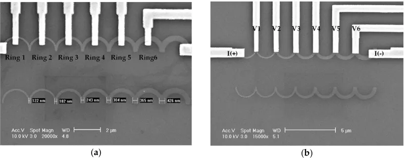
sputtering with collimator to reduce side wall effect. After cleaned the surface of specimens by Ar ion-milling, the I/V (Cu (75nm)/Au (5nm)) contact leads were also deposited by dc-magnetron sputtering in situ. The outer diameter of each half-ring is 2µm. The linewidth of half-ring corners is 120 nm to 370 nm with step ~50-60 nm. Two kind of voltage contact layouts were designed, one is in the middle of two corners another is on the corners, as shown in Figure 1. We name these two half-ring wires as middle-contact half-ring and corner-contact half-ring wires in the following text. In the MR measurements, the applied current was 10 µA, which was small enough to avoid thermal activation. We also used the micromagnet simulation software OOMMF [10] to simulate the spin configurations of all the samples.
(a) (b)
Figure 1. SEM micrograph of half-ring wires with I/V leads. (a) middle-contact half-ring wire; (b) corner-contact half-ring wire.
3. Results
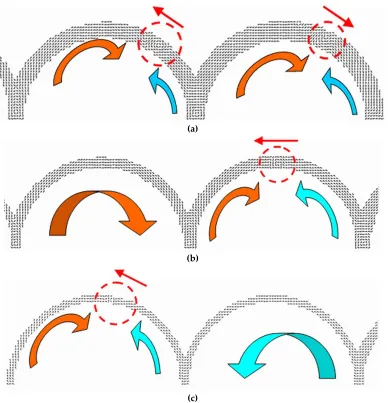
The longitudinal and transverse MR loops of two kinds of I/V contact half-ring wires, measuring from voltage contact 1 and 6, are shown in Figure 2. Apparently, in Figure 2 (a), there are five distinct jumps appeared in the longitudinal MR of middle-contact half-ring wire. In Figure 2 (c), six straight wires, 120 nm to 370 nm wide 30 nm thick and 3.0 µm long, connected in series were also fabricated, but no distinct jump appeared in this longitudinal MR loop. And in Figure 2 (b) and (d), there are no varied jumps appeared in the transverse MR of both middle- and corner-contact half-ring wires. To investigate these five jumps come from, we measured the MR by change different two voltage contacts, such as 1-5, 1-4 … to 1-2 (Figure 2 (e)), or 2-6, 3-6 … to 5-6. And two neighbor voltage contacts 1-2, 2-3 … to 5-6 were also measured. Figure 2 shows the maximum number of jumps is equal to the corners between the voltage contact leads. By all these measurements, we may infer these five jumps are resulting from domain wall nucleation, propagation, and annihilation on the five corners between six voltage contact leads during the magnetization reversal process. For the discontinuity of half-ring geometry and shape anisotropy, it costs less energy to nucleate domain wall on the corners. To reconfirm our explanation, the spin configuration of half-ring wire was simulated by micromagnet simulation program OOMMF. The simulations were based on the integration of the Landau-Lifshitz-Gilbert equation. The magnetic material Py parameters used for the simulations were a saturation magnetization Ms = 8.0×10⁵ A/m and an exchange constant A =
domain wall nucleation was taken place on the corner of widest corner between voltage contact 5 and 6 (or ring 5 and ring 6).
(a)
(b)
(c)
(d) (e)
Figure 2. Room temperature MR loops: (a)longitudinal (b) transverse MR of middle-contact half-ring wire; (c) longitudinal (d) transverse MR of corner-contact half-ring wire; (e) longitudinal MR of middle-contact half-ring wire with different voltage contact.
4 of 6
manifest jumps in the longitudinal MR loop of corner-contact half-ring wire as the middle-contact half-ring wire.
(a)
(b)
(c)
Figure 3. Simulation spin configuration around the switching of (a) ring 5 and 6, (b) ring 3 and 4, (c) ring 1 and 2, the small arrows indicate the propagation direction of domain wall (inside the dash circle), the orientation of magnetization is illustrated by the arrow under the rings.
The reasons are as follows. First, for the majority of electric current flow in the voltage contact lead rather than the corner of permalloy beneath, thus, to reduce the anisotropy magnetoresistance (AMR) contributed by the corner. Second, when the vortex wall propagates along the half-ring the change of resistance is very little. The negative AMR ratio is proportion to the regime where local magnetization is not parallel to the current. Obviously, the magnetization transient regime of domain wall is smaller than the corner. Third, the time for a domain wall pass through a half-ring is less than 1 ns calculated by domain wall mobility 31 ms-1Oe-1 [11], so it’s not easy to detect the AMR
4. Discussion
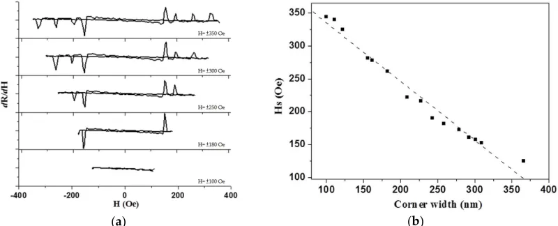
Figure 4 (a) shows the longitudinal minor loop of a differential MR (dR/dH) of a wider half-ring wire (corner width 150 nm – 370 nm) with voltage contact 1-6. The number of discrete jumps, like the digital signal, depends on the analogue signal of external field. Therefore, the half-ring wire can act like an ADC (analogue-digital converter) by transforming analogue signal (external field) into digital signal (number of jumps in differential MR loop). Figure 4 (b) shows the switching field versus linewidth of corner of 4 half-ring wires. Between the corner width from 100nm to 370nm, we made a simple linear fit from these data and obtained Hs = -0.89*(corner width in nm) + 427 ±10 (Oe). It’s reasonable as the width of corner become narrow (or sharp) the nucleation field of domain wall become large. We may interpret the magnetization reversal process of half-ring wires as the domain wall (soliton) [3] propagates through the ring (channel or path) then traps on the corner (pinning center or energy barrier), as the external field (driving force) reach to the switching field of this corner and the domain wall propagates again, and so on. Compare with the magnetization reversal, head-head onion state to vortex state to tail-tail onion state, of micromagnet in ring pattern [12,13].
The half-ring wires are six head to head semi-onion states in remanence from positive saturation. As the negative field increase, a jump in MR loop means one tail to tail semi-onion state increase and one head to head semi-onion state decrease. The corner of half-ring plays a role as the lock or notch for reverse the onion state, and the switching field is the key to open this lock.
(a) (b)
Figure 4. (a) The differential value of dR/dH versus H for the minor loop of wider half-ring wire with maximum 4 jumps; (b) The switching field versus corner width, the dash line is the result of a linear fit.
5. Conclusions
In summary, we present different width in-series half-ring wires in which the switching field or domain wall depinning field depends linearly on the corner width between 100nm to 370nm. This phenomenon of half-ring wire can be used as a micro- ADC- digital micro- magnetic meter. The energy consumption by this 5-bit half-ring digital micro- magnetic meter is about 1mW (p= I2/R) and
the reaction time is about 6 ns. We may expect that if this half-ring wire is fabricated in spin valve structure or the domain wall is driven by spin polarized current, the signal/noise ratio will increase, and the function will be versatile.
Funding: This work was supported by NCHU and Academia Sinica.
Acknowledgments: The authors would like to thank Dr. K. W. Cheng, Mr. Y. S. Chen, and M. T. Lin at Academia Sinica, for their assistance during the experimental measurements.
References
1. S. A. Wolf, D. D. Awschalom, R. A. Buhrman, J. M. Daughton, S. von Molnár, M.L. Roukes, A. Y. Chtchelkanova, and D. M. Treger, Science, 2001; 294, 1488.
2. T. Jungwirth, X. Marti, P. Wadley & J. Wunderlich, Nature Nanotechnology, 2016; 11, 231–241 3. D. A. Allwood, G. Xiong, and R. P. Cowburn, Appl. Phys. Lett, 2004; 85, 2848.
4. D. A. Allwood, Gang Xiong, C. C. Faulkner, D. Atkinson, D. Petit, and R. P. Cowburn, Science, 2005; 309, 1688.
5. D. A. Allwood, G. Xiong, and R. P. Cowburn, Appl. Phys. Lett, 2006; 89, 102504.
6. Yoko Yoshimura, Kab-Jin Kim, Takuya Taniguchi, Takayuki Tono, Kohei Ueda, Ryo Hiramatsu, Takahiro Moriyama, Keisuke Yamada, Yoshinobu Nakatani & Teruo Ono, Nature Physics, 2016; 12, 157–161. 7. Sasikanth Manipatruni, Dmitri E. Nikonov & Ian A. Young, Nature Physics, 2018; 14, 338–343 8. R. P. Cowburn, D. A. Allwood, Gang Xiong and M .D. Cooke, J.Appl.Phys, 2002; 91, 6949. 9. Eiji Saitoh, Hideki Miyajima, Takehiro Yamaoka, and Gen Tatara, Nature, 2004; 432, 203.
10. A 2-d code to calculate the magnetization configuration and its field evolution is described on http:/math.nist.gov/oommf.
11. D.Atkinson, D. A. Allwood, Gang Xiong, M .D. Cooke, C. C. Faulkner, and R. P. Cowburn, Nature Mater, 2003; 2, 85.
12. M. Kläui, C. A. F. Vaz J. A. C. Bland,L. J. Heyderman, F. Nolting, A. Pavlovska, E. Bauer, S. Cherifi, S. Heun and A. Locatelli, Appl. Phys. Lett, 2004; 85, 5637.