Influence on Structural, Optical & Solid
State Properties of Nickel Doped Cadmium
Sulfide Thin Films
V. B. Sanap1
Assistant Professor, Dept. of Physics, Yeshwantrao Chavan College, Sillod, Dist. Aurangabad (M.S.), India. 1
ABSTRACT- Nanocrystalline Cd1-xNixS thin films were prepared at 70±2ºC by a simple and inexpensive chemical
bath deposition (CBD) technique. These films have been deposited on commercial glass substrate for various nickel concentrations (i.e. x= 0, 0.3, 0.5. 0.7, 1). The effect of nickel content (x value) on structural, morphological, optical and solid state properties have been studied. The as-deposited films were characterized using X-ray diffractometer (X-PERT PRO), SEM and UV-VIS spectrophotometer. The obtained film shows good crystallinity with hexagonal structure. The average grain size estimated is 4.22nm. The values of energy bandgap, optical and solid state constants have been evaluated for varying Ni content for the study of various optoelectronic applications.
KEYWORDS: CdNiS, chemical bath deposition, thin films.
I. INTRODUCTION
In last few years, considerable interest has been shown in the synthesis of semiconducting nanocrystalline thin films for optoelectronic applications. Nanostructured materials based on II-VI group compounds have long been known to be suitable materials for photovoltaic device applications because of their high optical absorption coefficients [1]. The synthesis of ternary metal chalcogenides of group II-VI semiconductors in nanocrystalline form has been a rapidly growing area of research due to their important non-linear optical properties, luminescent properties, quantum confinement effect and other important chemical and physical properties.
Doped semiconductor nano-materials have attracted research interests in the recent years. These materials exhibit novel size dependent properties. Thus they are under active consideration as potential candidates for various optoelectronic applications. Nickel doped cadmium sulfide (Cd1-xNixS) have properties in between CdS and NiS.
CdNiS films have low resistivity in light and also have high transmittance in the visible region [2].
II. LITERATURE SURVEY
Addition of Ni to the most widely used CdS buffer layer material enhances the electronic and optical properties of optoelectronic devices. From the analysis, due to high bandgap Cd1-xNixS films were found to possess favorable
properties for solar and industrial applications such as antireflection coating in the solar collectors [3-4], solar control coatings, warming coatings as well as solar absorber layer of a solar cell [5]. Keeping these aspects in view, more attention is being given in producing good quality CdNiS thin films for comprehensive structural, optical studies and their various applications.
Cd1-xNixS thin film have been prepared using various techniques such as, spray pyrolysis, sputtering, electro
deposition, vacuum evaporation, chemical vapour deposition, chemical bath deposition (CBD), etc. Among these techniques, chemical bath deposition is simple, cost effective which yields uniform, adherent, stable and hard nanocrystalline films with good reproducibility as compared to the others for large-area solar cell fabrication [6-9]. In this study, we were prepared the Cd1-xNixS thin films for varying Ni content by simple CBD technique. The
III. EXPERIMENTAL DETAILS
The Cd1-xNixS thin films were prepared by CBD technique on commercial glass slide for various nickel
concentration (x= 0, 0.3, 0.5, 0.7, 1). The starting materials used were CdCl2 (1M) as a Cd2+ ion source, NiCl2 (x=
0, 0.3, 0.5, 0.7, 1M) as Ni2+ ion source, thiourea (1M) as an S2- ion source. An alkaline solution of ammonia was used to adjust pH of the reaction mixture. All the chemicals used were of Analytical Reagent grade. The process involving a controllable chemical reaction at a low rate, by adjusting the pH value and temperature of the working solution allows maintaining the stoichiometry constant for any ratio of anions and cations. The experimental arrangement consists of a special substrate holder which is attached to a motor having a constant speed of 60 r.p.m. The temperature of chemical bath was adjusted with a hot plate and temperature controller (72±2ºC), while magnetic stirrer is applied to promote ion-by-ion heterogeneous growth on the substrate. The Cd1-xNixS samples
were prepared on carefully cleaned glass substrates. Cleaning of substrate is important in deposition of thin films, cleaning steps and growth procedure is reported elsewhere [10-11]. As-deposited thin films were rinsed with distilled water and allowed to dry in air.
The grown films were characterized by (XPERT-PRO) X-ray diffractometer using Cu-Kα radiation with wavelength, 1.5418Å for the study of crystallographic structure. The thickness of thin film was measured by the weight difference method at room temperature. The average grain size in the deposited films was obtained from a Debye-Scherrer formula. Surface morphology was examined by JEOL model JSM-6400 scanning electron microscope (SEM). Optical properties were measured at room temperature by using Perklin-Elmer UV-VIS lambda-35 spectrometer in the wavelength range 300-1100nm.
IV. RESULTS AND DISCUSSIONS
1. Structural & Morphological properties
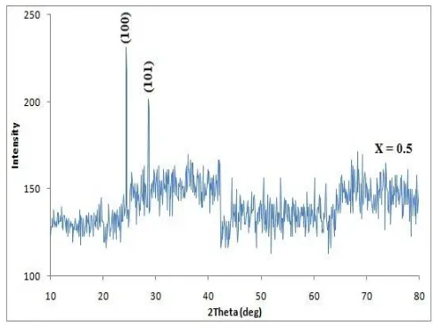
Figure 1 shows the XRD pattern of Cd1-xNixS films for Ni content x=0.5 A comparison of the peak position (2θ
values) of the JCPDS XRD spectra data suggests that the as-deposited films have hexagonal structure. The 2θ value of 24.54° (d= 3.6179 Å) and 28.72° (d = 3.0998 Å) correspond to the diffraction lines produced by (100) and (101) planes respectively [12].
Fig.1 XRD pattern of Cd1-xNixS films for x = 0.5
g = Kλ / β cosθ (1)
Where,
K = constant taken to be 0.94, λ = wavelength of X-ray used (1.542Å), β = FWHM of the peak and θ = Bragg’s angle.
The calculated average grain size of the film is about 4.22 nm.
Fig. 2 SEM of Cd1-xNixS films at x = 0.5
The SEM micrograph shows smoother and more uniform films (Figure 2). It is observed that the average grain size obtained from XRD matches with SEM and is about 4.22 nm.
2. Optical & Solid State properties
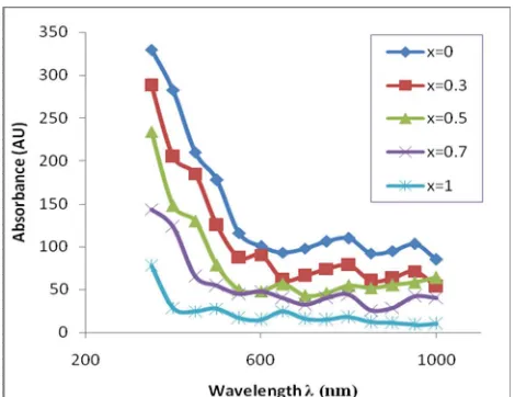
Figure 3 shows the plot of spectral absorbance of Cd1-xNixS thin films for varying Ni content. From the plot, it is
observed that the absorbance of Cd1-xNixS thin film decreases as the content of nickel in the film increases. This
high absorbing material is used for window coating, since it is capable of absorbing the harmful UV radiations and leaving the inside surface cool. It acts as convectional air-conditioner.
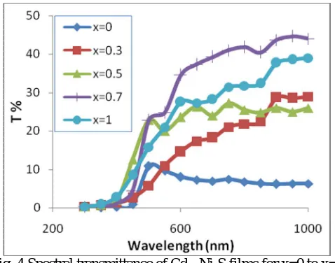
Fig. 4 Spectral transmittance of Cd1-xNixS films for x=0 to x=1
Figure 4 shows the plot of spectral transmittance of Cd1-xNixS thin film grown. From the plot it is observed that
CdNiS thin film has a high transmittance value in near infrared region (NIR) region whereas it is almost 0% in UV region. Plot shows, the value of transmittance for the deposited film increases as the Ni concentration increases. This makes the films suitable in the construction of poultry farms because it allows much infrared radiation to warm the chicks.
Figure 5 shows the plot of spectral reflectance of Cd1-xNixS thin film grown. From the plot, it is observed that the
reflectance is low across the UV, visible and near IR regions. This makes the film suitable for anti-reflection thin films which when used, improves the efficiency of the solar collector plates.
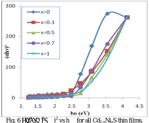
Fig. 6 Plot of (αh
)2 vs h
for all Cd1-xNixS thin films.The band gap energy was determined from absorbance data by plotting (αh
)2 versus h
(figure 6) and then extrapolating the straight line portion to the energy axis at α=0. The band gap energy Eg obtained for each Ni content is different. For higher Ni content (x=1) the band gap is 2.75 eV and for lower Ni content (x=0) it is 2.48 eV. The band gap of other films is intermediate.Table 1. Optical & solid state constants of Cd1-xNixS thin films prepared at various Ni content (x= 0 to 1)
Ni content
Energy bandgap
Eg (eV)
Average R.I.
n
Extinction coefficient
k
Dielectric
constants conductivity Optical σ x1013 S-1
Ɛr Ɛi
X=0 2.48 2.57 0.18 7.02 0.92 14.74
X=0.3 2.52 2.69 0.11 7.32 0.61 9.87
X=0.5 2.7 2.42 0.10 6.04 0.48 7.89
X=0.7 2.6 2.19 0.08 4.91 0.36 6.30
X=1 2.75 2.14 0.09 5.03 0.38 6.24
The optical and solid state constants of Cd1-xNixS films prepared at varying Ni content were evaluated. The
observed optical and solid state constants such as refractive index (n), extinction coefficient (k), dielectric constants (Ɛr , Ɛi ) as well as optical conductivity (σ) of the films were illustrated by table 1.
V. CONCLUSION
In this study, Cd1-xNixS nano-crystalline thin films have been grown successfully onto glass substrates using
4.22nm. The optical and solid state studies showed that the films have high absorbance in the UV region. This property makes the film for window coatings. The band gap energy obtained is in between 2.48eV and 2.72eV. The wider bandgap of the deposited films makes them suitable for optoelectronic devices, for instance window/absorber layer in solar cells.
REFERENCES
1. Ragesh Chandran, G.Suresh, Chalcogenide Letters Vol. 8, No. 11, p. 689 – 694, 2011
2. T PremKumar, S. Saravanakumar, K. Sankaranarayanan, Appl. Surf. Sci. 257, 1923–1927, 2011. 3. Theye M. Optical Properties of Thin Film (Butterworth’s and Co. London, UK) p 255, 1983.
4. Chopra K.L. and Malhotra, L.K. Thin Film Technology and Applications (Tata McGraw Hill: New Delhi, India) 3 p 237-249, 1985. 5. Ezema, F.I. “Effect of Deposition Time on the Band Gap and Optical Properties of Chemical Bath Deposited CdNiS Thin Films”,
Optoelectronics and Advanced Material-Rapid Communications 3 (2) p 141-144, 2009. 6. J.M. Dona, J. Herrero Thin Solid Films p 5-12, 1995.
7. Saliha Ilican, Muhsin Zor et al Optica Applicata, XXXVI 1, 2006.
8. D.N. Okoli, A.J. Ekpunobi and C.E. Okeke ,Academic Open Internet Journal, 18, 2006. 9. P.K.Nair, M.T.S. Nair et al, J. Phys D22 p 829, 1989.
10. V.B.Sanap, B.H.Pawar, “Growth and characterization of nanostructured Cds thin films by chemical bath deposition technique”, Chalcogenide Letters 6(8) p 415-419, 2009.
11. V.B.Sanap, B.H.Pawar, “Optical study of effect of cadmium sources on nanocrystalline cds thin films”,Chalcogenide Letters 7(3) p 227-231, 2010.
12. Ates, M. A. Yildirim, M. Kundaki, M. Yildirim, Chinese J. of Phys 45, 2, 2001. 13. Jiyon Song, Sheng S Li et al, IEEE p 449-452, 2005.
14. S. C. Ezugwu, F. I. Ezema, et al, Optoelectronics And Advanced Materials – Rapid Communications 3(2) p 141 – 144, 2009.
15. Ottih, I.E. and A.J. Ekpunobi, “Fabrication and Characterization of High Efficiency Solar Cell Thin Films (CdNiS)”, Pacific Journal of Science and Technology 12(1) p 351-355, 2011.