ABSTRACT
BAE, CHOELHWYI. GaN-dielectric interface formation for gate dielectrics and passivation layers using remote plasma processing. (Under the direction of Professor Gerald Lucovsky)
In previous studies, device quality Si-SiO2 interfaces and dielectric bulk films
(SiO2) were prepared using a two-step process; i) remote plasma-assisted oxidation
(RPAO) to form a superficially interfacial oxide (~0.6 nm) and ii) remote plasma
enhanced chemical vapor deposition (RPECVD) to deposit the oxide film. The same
approach has been applied to the GaN-SiO2 system. After a 300 oC remote N2/He plasma
treatment of the GaN surface, residual C and Cl were reduced below Auger electron
spectroscopy (AES) detection, and the AES peak ratio of O KLL and N KLL was ~0.06 or
~0.1 monolayer of oxygen. RPAO of GaN surfaces using O2, N2O, and N2O in N2 source
gases were investigated by on-line AES to determine the oxidation kinetics and chemical
composition of the interfacial oxide. Without an RPAO step, subcutaneous oxidation of
GaN takes place during RPECVD deposition of SiO2, and on-line AES indicates a ~0.7
nm subcutaneous oxide. Compared to single step SiO2 deposition, significantly reduced
interface state density (Dit) was obtained at the GaN-SiO2 interface by independent
control of GaN-Ga2O3 interface formation by thin RPAO oxide (~1 nm) and SiO2 film
deposition by RPECVD. High-low frequency method and conductance method indicate
that Dit of GaN Metal-Oxide-Semiconductor (MOS) sample without RPAO is ~5 times
larger than that of the sample with RPAO. For the GaN MOS structure with remote
plasma-assisted oxidation and nitridation, determined values of Dit were in the range of
low-to-mid x 1011 cm-2eV-1. Also, we report on high temperature and photo-assisted
GaN-DIELECTRIC INTERFACE FORMATION
FOR GATE DIELECTRICS AND PASSIVATION LAYERS
USING REMOTE PLASMA PROCESSING
by
CHOELHWYI BAE
A dissertation submitted to the Graduate Faculty of
North Carolina State University
in partial fulfillment of the requirements for
the Degree of Doctor of Philosophy
ELECTRICAL AND COMPUTER ENGINEERING
Raleigh, North Carolina
May 2003
Approved by:
Prof. V. Misra
Prof. C. M. Osburn Prof. R. F. Davis
Prof. J. R. Hauser Prof. G. Lucovsky
BIOGRAPHY
Choelhwyi Bae was born in Seoul, South Korea on May 21, 1970 to Sun-Tae Bae and
Sook-Jae Oh. He obtained his B. S. degree in Metallurgical Engineering, Hanyang
University, Seoul, South Korea in 1995. After his undergraduate study, he joined the joint
program between the Korea Institute of Science and Technology (KIST), Seoul, South
Korea and Hanyang University, Seoul, South Korea. He studied about “abnormal grain
growth of Nb-doped SrTiO3” in Dielectric Research Laboratory, Division of Ceramics,
KIST, and obtained his M. S. degree in Surface Science Laboratory, Metallurgical
Engineering, Hanyang University in 1997. From March 1997 to August 1998, he worked
at Thin Film Technology Research Center, KIST, Seoul, South Korea. He assembled R.F.
magnetron sputtering cluster and investigated about “abnormal grain growth and oriented
growth of SrBi2Ta2O9 thin films fabricated by R.F. magnetron sputtering”. In August
1998, he proceeded to the United States and enrolled in the Ph. D. program at North
Carolina State University, Raleigh. He designed and assembled “ultra high vacuum
(UHV) wafer bonding chamber” in Surface Science Laboratory, Material Science and
Engineering. After he joined the Electrical and Computer Engineering program in
January 2000, he investigated “GaN-dielectric interface formation for gate dielectrics and
passivation layers using remote plasma processing” under the guidance of Professor
ACKNOWLEDGEMENTS
First I would like to express my appreciation to my advisor, Professor G. Lucovsky. His
knowledge makes me work with confidence, and his endurance makes me play this
research as my own game. I also remember and believe his encouragement “student
usually shows exponential growth in his research and you already turned corner”.
I would like to thank Professor J. R. Hauser (co-chair) for his helpful comments and
efforts in reading this manuscript. I am grateful to Professor C. Osburn, Professor R. F.
Davis, and Professor V. Misra for serving on my Ph. D. advisory committee.
I want to thank to the former and current Professor G. Lucovsky students. In particular, I
would like to express my gratitude to Dr. S. Hattangady and Dr. H. Nimi who assembled
‘2-inch cluster tool for remote plasma processing’. Also, I am grateful to S.-J. Oh for his
helpful proofreading of this manuscript.
Of course, I would like to thank to the staff of the NCSU Microelectronics Laboratory. I
really appreciate all the advice of my ‘vice-advisor’ J. O’Sullivan who helped me button
by button to use clean room equipment, especially antique R-H evaporator.
Finally, my deepest thanks go to my parent who miss their lovely son across the Pacific
TABLE OF CONTENTS
LIST OF TABLES ⋅⋅⋅⋅⋅⋅⋅⋅⋅⋅⋅⋅⋅⋅⋅⋅⋅⋅⋅⋅⋅⋅⋅⋅⋅⋅⋅⋅⋅⋅⋅⋅⋅⋅⋅⋅⋅⋅⋅⋅⋅⋅⋅⋅⋅⋅⋅⋅⋅⋅⋅⋅⋅⋅⋅⋅⋅⋅⋅⋅⋅⋅⋅⋅⋅⋅⋅⋅⋅⋅⋅⋅⋅⋅⋅⋅⋅⋅⋅⋅⋅⋅⋅⋅⋅⋅⋅⋅⋅⋅⋅⋅⋅⋅⋅⋅⋅⋅⋅⋅ vii
LIST OF FIGURES ⋅⋅⋅⋅⋅⋅⋅⋅⋅⋅⋅⋅⋅⋅⋅⋅⋅⋅⋅⋅⋅⋅⋅⋅⋅⋅⋅⋅⋅⋅⋅⋅⋅⋅⋅⋅⋅⋅⋅⋅⋅⋅⋅⋅⋅⋅⋅⋅⋅⋅⋅⋅⋅⋅⋅⋅⋅⋅⋅⋅⋅⋅⋅⋅⋅⋅⋅⋅⋅⋅⋅⋅⋅⋅⋅⋅⋅⋅⋅⋅⋅⋅⋅⋅⋅⋅⋅⋅⋅⋅⋅⋅⋅⋅⋅⋅⋅⋅ viii
1. INTRODUCTION 1.1 INTRODUCTION ⋅⋅⋅⋅⋅⋅⋅⋅⋅⋅⋅⋅⋅⋅⋅⋅⋅⋅⋅⋅⋅⋅⋅⋅⋅⋅⋅⋅⋅⋅⋅⋅⋅⋅⋅⋅⋅⋅⋅⋅⋅⋅⋅⋅⋅⋅⋅⋅⋅⋅⋅⋅⋅⋅⋅⋅⋅⋅⋅⋅⋅⋅⋅⋅⋅⋅⋅⋅⋅⋅⋅⋅⋅⋅⋅⋅⋅⋅⋅⋅⋅⋅⋅⋅⋅⋅⋅⋅⋅⋅⋅⋅ 1
1.1.1 Remote plasma processing for gate dielectric insulators ⋅⋅⋅⋅⋅⋅⋅⋅⋅⋅⋅⋅⋅⋅⋅⋅⋅⋅⋅⋅⋅⋅⋅⋅ 1
1.1.2 Compatibility of remote plasma-assisted oxidation with GaN ⋅⋅⋅⋅⋅⋅⋅⋅⋅⋅⋅⋅⋅⋅⋅ 2
1.1.3 GaN-dielectric insulator interface for gate dielectrics/passivation ⋅⋅⋅⋅⋅⋅⋅⋅ 3
1.2 APPROACH ⋅⋅⋅⋅⋅⋅⋅⋅⋅⋅⋅⋅⋅⋅⋅⋅⋅⋅⋅⋅⋅⋅⋅⋅⋅⋅⋅⋅⋅⋅⋅⋅⋅⋅⋅⋅⋅⋅⋅⋅⋅⋅⋅⋅⋅⋅⋅⋅⋅⋅⋅⋅⋅⋅⋅⋅⋅⋅⋅⋅⋅⋅⋅⋅⋅⋅⋅⋅⋅⋅⋅⋅⋅⋅⋅⋅⋅⋅⋅⋅⋅⋅⋅⋅⋅⋅⋅⋅⋅⋅⋅⋅⋅⋅⋅⋅⋅⋅⋅⋅⋅ 5
1.2.1 Apparatus ⋅⋅⋅⋅⋅⋅⋅⋅⋅⋅⋅⋅⋅⋅⋅⋅⋅⋅⋅⋅⋅⋅⋅⋅⋅⋅⋅⋅⋅⋅⋅⋅⋅⋅⋅⋅⋅⋅⋅⋅⋅⋅⋅⋅⋅⋅⋅⋅⋅⋅⋅⋅⋅⋅⋅⋅⋅⋅⋅⋅⋅⋅⋅⋅⋅⋅⋅⋅⋅⋅⋅⋅⋅⋅⋅⋅⋅⋅⋅⋅⋅⋅⋅⋅⋅⋅⋅⋅⋅⋅⋅⋅⋅⋅⋅⋅ 6
1.2.2 Two (or multi)-step process ⋅⋅⋅⋅⋅⋅⋅⋅⋅⋅⋅⋅⋅⋅⋅⋅⋅⋅⋅⋅⋅⋅⋅⋅⋅⋅⋅⋅⋅⋅⋅⋅⋅⋅⋅⋅⋅⋅⋅⋅⋅⋅⋅⋅⋅⋅⋅⋅⋅⋅⋅⋅⋅⋅⋅⋅⋅⋅⋅⋅⋅⋅⋅⋅⋅⋅⋅⋅ 7
1.3 OVERVIEW OF DISSERTATION ⋅⋅⋅⋅⋅⋅⋅⋅⋅⋅⋅⋅⋅⋅⋅⋅⋅⋅⋅⋅⋅⋅⋅⋅⋅⋅⋅⋅⋅⋅⋅⋅⋅⋅⋅⋅⋅⋅⋅⋅⋅⋅⋅⋅⋅⋅⋅⋅⋅⋅⋅⋅⋅⋅⋅⋅⋅⋅⋅⋅⋅⋅⋅⋅⋅⋅ 7
1.4 REFERENCES ⋅⋅⋅⋅⋅⋅⋅⋅⋅⋅⋅⋅⋅⋅⋅⋅⋅⋅⋅⋅⋅⋅⋅⋅⋅⋅⋅⋅⋅⋅⋅⋅⋅⋅⋅⋅⋅⋅⋅⋅⋅⋅⋅⋅⋅⋅⋅⋅⋅⋅⋅⋅⋅⋅⋅⋅⋅⋅⋅⋅⋅⋅⋅⋅⋅⋅⋅⋅⋅⋅⋅⋅⋅⋅⋅⋅⋅⋅⋅⋅⋅⋅⋅⋅⋅⋅⋅⋅⋅⋅⋅⋅⋅⋅⋅⋅⋅ 8
2. REVIEW OF n-GaN METAL-INSULATOR-SEMICONDUCTROR (MIS) SYSTEMS AND PROPER ANALYSIS 2.1 REVIEW OF n-GAN MIS CAPACITORS ⋅⋅⋅⋅⋅⋅⋅⋅⋅⋅⋅⋅⋅⋅⋅⋅⋅⋅⋅⋅⋅⋅⋅⋅⋅⋅⋅⋅⋅⋅⋅⋅⋅⋅⋅⋅⋅⋅⋅⋅⋅⋅⋅⋅⋅⋅⋅⋅⋅⋅⋅⋅ 12
2.1.1 SiO2 ⋅⋅⋅⋅⋅⋅⋅⋅⋅⋅⋅⋅⋅⋅⋅⋅⋅⋅⋅⋅⋅⋅⋅⋅⋅⋅⋅⋅⋅⋅⋅⋅⋅⋅⋅⋅⋅⋅⋅⋅⋅⋅⋅⋅⋅⋅⋅⋅⋅⋅⋅⋅⋅⋅⋅⋅⋅⋅⋅⋅⋅⋅⋅⋅⋅⋅⋅⋅⋅⋅⋅⋅⋅⋅⋅⋅⋅⋅⋅⋅⋅⋅⋅⋅⋅⋅⋅⋅⋅⋅⋅⋅⋅⋅⋅⋅⋅⋅⋅⋅⋅⋅⋅ 12
2.1.2 Si3N4 ⋅⋅⋅⋅⋅⋅⋅⋅⋅⋅⋅⋅⋅⋅⋅⋅⋅⋅⋅⋅⋅⋅⋅⋅⋅⋅⋅⋅⋅⋅⋅⋅⋅⋅⋅⋅⋅⋅⋅⋅⋅⋅⋅⋅⋅⋅⋅⋅⋅⋅⋅⋅⋅⋅⋅⋅⋅⋅⋅⋅⋅⋅⋅⋅⋅⋅⋅⋅⋅⋅⋅⋅⋅⋅⋅⋅⋅⋅⋅⋅⋅⋅⋅⋅⋅⋅⋅⋅⋅⋅⋅⋅⋅⋅⋅⋅⋅⋅⋅⋅⋅ 13
2.1.3 Ga2O3/SiO2 and SiO2/Si3N4/SiO2 ⋅⋅⋅⋅⋅⋅⋅⋅⋅⋅⋅⋅⋅⋅⋅⋅⋅⋅⋅⋅⋅⋅⋅⋅⋅⋅⋅⋅⋅⋅⋅⋅⋅⋅⋅⋅⋅⋅⋅⋅⋅⋅⋅⋅⋅⋅⋅⋅⋅⋅⋅⋅⋅⋅⋅⋅⋅ 14
2.1.4 Ga2O3 ⋅⋅⋅⋅⋅⋅⋅⋅⋅⋅⋅⋅⋅⋅⋅⋅⋅⋅⋅⋅⋅⋅⋅⋅⋅⋅⋅⋅⋅⋅⋅⋅⋅⋅⋅⋅⋅⋅⋅⋅⋅⋅⋅⋅⋅⋅⋅⋅⋅⋅⋅⋅⋅⋅⋅⋅⋅⋅⋅⋅⋅⋅⋅⋅⋅⋅⋅⋅⋅⋅⋅⋅⋅⋅⋅⋅⋅⋅⋅⋅⋅⋅⋅⋅⋅⋅⋅⋅⋅⋅⋅⋅⋅⋅⋅⋅⋅⋅⋅⋅ 14
2.1.5 Other dielectric insulators ⋅⋅⋅⋅⋅⋅⋅⋅⋅⋅⋅⋅⋅⋅⋅⋅⋅⋅⋅⋅⋅⋅⋅⋅⋅⋅⋅⋅⋅⋅⋅⋅⋅⋅⋅⋅⋅⋅⋅⋅⋅⋅⋅⋅⋅⋅⋅⋅⋅⋅⋅⋅⋅⋅⋅⋅⋅⋅⋅⋅⋅⋅⋅⋅⋅⋅⋅⋅ 15
2.2 REVIEW OF n-GaN MISFETs ⋅⋅⋅⋅⋅⋅⋅⋅⋅⋅⋅⋅⋅⋅⋅⋅⋅⋅⋅⋅⋅⋅⋅⋅⋅⋅⋅⋅⋅⋅⋅⋅⋅⋅⋅⋅⋅⋅⋅⋅⋅⋅⋅⋅⋅⋅⋅⋅⋅⋅⋅⋅⋅⋅⋅⋅⋅⋅⋅⋅⋅⋅⋅⋅⋅⋅⋅⋅⋅⋅ 16
2.3 MIS SYSTEM ANALYSIS IN WIDE BAND GAP SEMICONDUCTOR ⋅⋅ 17
2.3.1 Deepest measurable interface state and response time of interface ⋅⋅⋅⋅⋅⋅ 17
2.3.2 Limitation of high frequency C-V method at room temperature ⋅⋅⋅⋅⋅⋅⋅⋅⋅⋅ 19
2.3.3 Photo-assisted C-V method at room temperature ⋅⋅⋅⋅⋅⋅⋅⋅⋅⋅⋅⋅⋅⋅⋅⋅⋅⋅⋅⋅⋅⋅⋅⋅⋅⋅⋅⋅⋅⋅⋅⋅⋅⋅ 20
2.3.4 Conductance method at high temperature ⋅⋅⋅⋅⋅⋅⋅⋅⋅⋅⋅⋅⋅⋅⋅⋅⋅⋅⋅⋅⋅⋅⋅⋅⋅⋅⋅⋅⋅⋅⋅⋅⋅⋅⋅⋅⋅⋅⋅⋅⋅⋅⋅⋅ 22
2.4 REFERENCES ⋅⋅⋅⋅⋅⋅⋅⋅⋅⋅⋅⋅⋅⋅⋅⋅⋅⋅⋅⋅⋅⋅⋅⋅⋅⋅⋅⋅⋅⋅⋅⋅⋅⋅⋅⋅⋅⋅⋅⋅⋅⋅⋅⋅⋅⋅⋅⋅⋅⋅⋅⋅⋅⋅⋅⋅⋅⋅⋅⋅⋅⋅⋅⋅⋅⋅⋅⋅⋅⋅⋅⋅⋅⋅⋅⋅⋅⋅⋅⋅⋅⋅⋅⋅⋅⋅⋅⋅⋅⋅⋅⋅⋅⋅⋅ 22
3. REMOTE PLASMA-ASSISTED OXIDATION OF GaN FOR LOW DEFECT DENSITY GaN-SiO2 INTERFACES 3.1 INTRODUCTION ⋅⋅⋅⋅⋅⋅⋅⋅⋅⋅⋅⋅⋅⋅⋅⋅⋅⋅⋅⋅⋅⋅⋅⋅⋅⋅⋅⋅⋅⋅⋅⋅⋅⋅⋅⋅⋅⋅⋅⋅⋅⋅⋅⋅⋅⋅⋅⋅⋅⋅⋅⋅⋅⋅⋅⋅⋅⋅⋅⋅⋅⋅⋅⋅⋅⋅⋅⋅⋅⋅⋅⋅⋅⋅⋅⋅⋅⋅⋅⋅⋅⋅⋅⋅⋅⋅⋅⋅⋅⋅ 26
3.2 EXPERIMENTAL ⋅⋅⋅⋅⋅⋅⋅⋅⋅⋅⋅⋅⋅⋅⋅⋅⋅⋅⋅⋅⋅⋅⋅⋅⋅⋅⋅⋅⋅⋅⋅⋅⋅⋅⋅⋅⋅⋅⋅⋅⋅⋅⋅⋅⋅⋅⋅⋅⋅⋅⋅⋅⋅⋅⋅⋅⋅⋅⋅⋅⋅⋅⋅⋅⋅⋅⋅⋅⋅⋅⋅⋅⋅⋅⋅⋅⋅⋅⋅⋅⋅⋅⋅⋅⋅⋅⋅⋅⋅⋅ 29
3.3.1 Subcutaneous oxidation of GaN during deposition of SiO2 ⋅⋅⋅⋅⋅⋅⋅⋅⋅⋅⋅⋅⋅⋅⋅⋅⋅ 31
3.3.2 GaN MOS system with/ without RPAO ⋅⋅⋅⋅⋅⋅⋅⋅⋅⋅⋅⋅⋅⋅⋅⋅⋅⋅⋅⋅⋅⋅⋅⋅⋅⋅⋅⋅⋅⋅⋅⋅⋅⋅⋅⋅⋅⋅⋅⋅⋅⋅⋅⋅⋅⋅ 33
3.3.3 High temperature and photo-assisted C-V measurements ⋅⋅⋅⋅⋅⋅⋅⋅⋅⋅⋅⋅⋅⋅⋅⋅⋅⋅⋅⋅ 38
3.4 SUMMARY ⋅⋅⋅⋅⋅⋅⋅⋅⋅⋅⋅⋅⋅⋅⋅⋅⋅⋅⋅⋅⋅⋅⋅⋅⋅⋅⋅⋅⋅⋅⋅⋅⋅⋅⋅⋅⋅⋅⋅⋅⋅⋅⋅⋅⋅⋅⋅⋅⋅⋅⋅⋅⋅⋅⋅⋅⋅⋅⋅⋅⋅⋅⋅⋅⋅⋅⋅⋅⋅⋅⋅⋅⋅⋅⋅⋅⋅⋅⋅⋅⋅⋅⋅⋅⋅⋅⋅⋅⋅⋅⋅⋅⋅⋅⋅⋅⋅⋅⋅ 39
3.5 REFERENCES ⋅⋅⋅⋅⋅⋅⋅⋅⋅⋅⋅⋅⋅⋅⋅⋅⋅⋅⋅⋅⋅⋅⋅⋅⋅⋅⋅⋅⋅⋅⋅⋅⋅⋅⋅⋅⋅⋅⋅⋅⋅⋅⋅⋅⋅⋅⋅⋅⋅⋅⋅⋅⋅⋅⋅⋅⋅⋅⋅⋅⋅⋅⋅⋅⋅⋅⋅⋅⋅⋅⋅⋅⋅⋅⋅⋅⋅⋅⋅⋅⋅⋅⋅⋅⋅⋅⋅⋅⋅⋅⋅⋅⋅⋅⋅ 40
4. REMOTE PLASMA-ASSISTED OXIDATION OF GaN AND NITROGEN INCORPORATION 4.1 INTRODUCTION ⋅⋅⋅⋅⋅⋅⋅⋅⋅⋅⋅⋅⋅⋅⋅⋅⋅⋅⋅⋅⋅⋅⋅⋅⋅⋅⋅⋅⋅⋅⋅⋅⋅⋅⋅⋅⋅⋅⋅⋅⋅⋅⋅⋅⋅⋅⋅⋅⋅⋅⋅⋅⋅⋅⋅⋅⋅⋅⋅⋅⋅⋅⋅⋅⋅⋅⋅⋅⋅⋅⋅⋅⋅⋅⋅⋅⋅⋅⋅⋅⋅⋅⋅⋅⋅⋅⋅⋅⋅⋅ 61
4.2 EXPERIMENTAL ⋅⋅⋅⋅⋅⋅⋅⋅⋅⋅⋅⋅⋅⋅⋅⋅⋅⋅⋅⋅⋅⋅⋅⋅⋅⋅⋅⋅⋅⋅⋅⋅⋅⋅⋅⋅⋅⋅⋅⋅⋅⋅⋅⋅⋅⋅⋅⋅⋅⋅⋅⋅⋅⋅⋅⋅⋅⋅⋅⋅⋅⋅⋅⋅⋅⋅⋅⋅⋅⋅⋅⋅⋅⋅⋅⋅⋅⋅⋅⋅⋅⋅⋅⋅⋅⋅⋅⋅⋅ 62
4.3 OXIDATION RATE USING ON-LINE AES ⋅⋅⋅⋅⋅⋅⋅⋅⋅⋅⋅⋅⋅⋅⋅⋅⋅⋅⋅⋅⋅⋅⋅⋅⋅⋅⋅⋅⋅⋅⋅⋅⋅⋅⋅⋅⋅⋅⋅⋅⋅⋅⋅⋅⋅⋅⋅⋅ 64
4.4 RESULTS AND DISCUSSION ⋅⋅⋅⋅⋅⋅⋅⋅⋅⋅⋅⋅⋅⋅⋅⋅⋅⋅⋅⋅⋅⋅⋅⋅⋅⋅⋅⋅⋅⋅⋅⋅⋅⋅⋅⋅⋅⋅⋅⋅⋅⋅⋅⋅⋅⋅⋅⋅⋅⋅⋅⋅⋅⋅⋅⋅⋅⋅⋅⋅⋅⋅⋅⋅⋅⋅⋅⋅⋅ 66
4.4.1 Remote O2/He plasma oxidation: pure GaOx/GaN system ⋅⋅⋅⋅⋅⋅⋅⋅⋅⋅⋅⋅⋅⋅⋅⋅⋅⋅ 66
4.4.2 Remote N2O/He (or N2/N2O/He) plasma oxidation: nitrogen incorporation ⋅⋅⋅⋅⋅⋅⋅⋅⋅⋅⋅⋅⋅⋅⋅⋅⋅⋅⋅⋅⋅⋅⋅⋅⋅⋅⋅⋅⋅⋅⋅⋅⋅⋅⋅⋅⋅⋅⋅⋅⋅⋅⋅⋅⋅⋅⋅⋅⋅⋅⋅⋅⋅⋅⋅⋅⋅⋅⋅⋅⋅⋅⋅⋅⋅⋅⋅⋅⋅⋅⋅⋅⋅⋅⋅⋅⋅⋅⋅⋅⋅⋅⋅⋅⋅⋅⋅ 67
4.4.3 Remote N2/He plasma nitridation of GaOx: enhanced nitrogen incorporation ⋅⋅⋅⋅⋅⋅⋅⋅⋅⋅⋅⋅⋅⋅⋅⋅⋅⋅⋅⋅⋅⋅⋅⋅⋅⋅⋅⋅⋅⋅⋅⋅⋅⋅⋅⋅⋅⋅⋅⋅⋅⋅⋅⋅⋅⋅⋅⋅⋅⋅⋅⋅⋅⋅⋅⋅⋅⋅⋅⋅⋅⋅⋅⋅⋅⋅⋅⋅⋅⋅⋅⋅⋅⋅⋅⋅⋅⋅⋅⋅⋅⋅⋅⋅⋅⋅ 69
4.4.4 Interface quality of GaN MOS system ⋅⋅⋅⋅⋅⋅⋅⋅⋅⋅⋅⋅⋅⋅⋅⋅⋅⋅⋅⋅⋅⋅⋅⋅⋅⋅⋅⋅⋅⋅⋅⋅⋅⋅⋅⋅⋅⋅⋅⋅⋅⋅⋅⋅⋅⋅⋅⋅⋅ 70
4.5 SUMMARY ⋅⋅⋅⋅⋅⋅⋅⋅⋅⋅⋅⋅⋅⋅⋅⋅⋅⋅⋅⋅⋅⋅⋅⋅⋅⋅⋅⋅⋅⋅⋅⋅⋅⋅⋅⋅⋅⋅⋅⋅⋅⋅⋅⋅⋅⋅⋅⋅⋅⋅⋅⋅⋅⋅⋅⋅⋅⋅⋅⋅⋅⋅⋅⋅⋅⋅⋅⋅⋅⋅⋅⋅⋅⋅⋅⋅⋅⋅⋅⋅⋅⋅⋅⋅⋅⋅⋅⋅⋅⋅⋅⋅⋅⋅⋅⋅⋅⋅⋅⋅ 71
4.6 REFERENCES ⋅⋅⋅⋅⋅⋅⋅⋅⋅⋅⋅⋅⋅⋅⋅⋅⋅⋅⋅⋅⋅⋅⋅⋅⋅⋅⋅⋅⋅⋅⋅⋅⋅⋅⋅⋅⋅⋅⋅⋅⋅⋅⋅⋅⋅⋅⋅⋅⋅⋅⋅⋅⋅⋅⋅⋅⋅⋅⋅⋅⋅⋅⋅⋅⋅⋅⋅⋅⋅⋅⋅⋅⋅⋅⋅⋅⋅⋅⋅⋅⋅⋅⋅⋅⋅⋅⋅⋅⋅⋅⋅⋅⋅⋅⋅⋅ 72
5. LOW TEMPERATURE REMOTE N2/He PLASMA-ASSISTED CLEANING OF GaN SURFACE 5.1 INTRODUCTION ⋅⋅⋅⋅⋅⋅⋅⋅⋅⋅⋅⋅⋅⋅⋅⋅⋅⋅⋅⋅⋅⋅⋅⋅⋅⋅⋅⋅⋅⋅⋅⋅⋅⋅⋅⋅⋅⋅⋅⋅⋅⋅⋅⋅⋅⋅⋅⋅⋅⋅⋅⋅⋅⋅⋅⋅⋅⋅⋅⋅⋅⋅⋅⋅⋅⋅⋅⋅⋅⋅⋅⋅⋅⋅⋅⋅⋅⋅⋅⋅⋅⋅⋅⋅⋅⋅⋅⋅⋅⋅ 93
5.2 EXPERIMENTAL ⋅⋅⋅⋅⋅⋅⋅⋅⋅⋅⋅⋅⋅⋅⋅⋅⋅⋅⋅⋅⋅⋅⋅⋅⋅⋅⋅⋅⋅⋅⋅⋅⋅⋅⋅⋅⋅⋅⋅⋅⋅⋅⋅⋅⋅⋅⋅⋅⋅⋅⋅⋅⋅⋅⋅⋅⋅⋅⋅⋅⋅⋅⋅⋅⋅⋅⋅⋅⋅⋅⋅⋅⋅⋅⋅⋅⋅⋅⋅⋅⋅⋅⋅⋅⋅⋅⋅⋅⋅ 95
5.3 RESULTS AND DISCUSSION ⋅⋅⋅⋅⋅⋅⋅⋅⋅⋅⋅⋅⋅⋅⋅⋅⋅⋅⋅⋅⋅⋅⋅⋅⋅⋅⋅⋅⋅⋅⋅⋅⋅⋅⋅⋅⋅⋅⋅⋅⋅⋅⋅⋅⋅⋅⋅⋅⋅⋅⋅⋅⋅⋅⋅⋅⋅⋅⋅⋅⋅⋅⋅⋅⋅⋅⋅⋅⋅ 97
5.3.1 Low temperature remote plasma-assisted cleaning of GaN surface ⋅⋅⋅⋅ 97
5.3.2 Effect of surface cleaning method on interface state density ⋅⋅⋅⋅⋅⋅⋅⋅⋅⋅⋅⋅⋅⋅⋅ 99
5.4 SUMMARY ⋅⋅⋅⋅⋅⋅⋅⋅⋅⋅⋅⋅⋅⋅⋅⋅⋅⋅⋅⋅⋅⋅⋅⋅⋅⋅⋅⋅⋅⋅⋅⋅⋅⋅⋅⋅⋅⋅⋅⋅⋅⋅⋅⋅⋅⋅⋅⋅⋅⋅⋅⋅⋅⋅⋅⋅⋅⋅⋅⋅⋅⋅⋅⋅⋅⋅⋅⋅⋅⋅⋅⋅⋅⋅⋅⋅⋅⋅⋅⋅⋅⋅⋅⋅⋅⋅⋅⋅⋅⋅⋅⋅⋅⋅⋅⋅⋅⋅ 101
5.5 REFERENCES ⋅⋅⋅⋅⋅⋅⋅⋅⋅⋅⋅⋅⋅⋅⋅⋅⋅⋅⋅⋅⋅⋅⋅⋅⋅⋅⋅⋅⋅⋅⋅⋅⋅⋅⋅⋅⋅⋅⋅⋅⋅⋅⋅⋅⋅⋅⋅⋅⋅⋅⋅⋅⋅⋅⋅⋅⋅⋅⋅⋅⋅⋅⋅⋅⋅⋅⋅⋅⋅⋅⋅⋅⋅⋅⋅⋅⋅⋅⋅⋅⋅⋅⋅⋅⋅⋅⋅⋅⋅⋅⋅⋅⋅⋅ 102
6. INTERFACE PROPERTIES OF n-GaN/SiO2 MOS STRUCTURE WITH REMOTE PLASMA-ASSISTED OXIDATION AND NITRIDATION 6.1 INTRODUCTION ⋅⋅⋅⋅⋅⋅⋅⋅⋅⋅⋅⋅⋅⋅⋅⋅⋅⋅⋅⋅⋅⋅⋅⋅⋅⋅⋅⋅⋅⋅⋅⋅⋅⋅⋅⋅⋅⋅⋅⋅⋅⋅⋅⋅⋅⋅⋅⋅⋅⋅⋅⋅⋅⋅⋅⋅⋅⋅⋅⋅⋅⋅⋅⋅⋅⋅⋅⋅⋅⋅⋅⋅⋅⋅⋅⋅⋅⋅⋅⋅⋅⋅⋅⋅⋅⋅⋅⋅ 116
6.2 EXPERIMENTAL ⋅⋅⋅⋅⋅⋅⋅⋅⋅⋅⋅⋅⋅⋅⋅⋅⋅⋅⋅⋅⋅⋅⋅⋅⋅⋅⋅⋅⋅⋅⋅⋅⋅⋅⋅⋅⋅⋅⋅⋅⋅⋅⋅⋅⋅⋅⋅⋅⋅⋅⋅⋅⋅⋅⋅⋅⋅⋅⋅⋅⋅⋅⋅⋅⋅⋅⋅⋅⋅⋅⋅⋅⋅⋅⋅⋅⋅⋅⋅⋅⋅⋅⋅⋅⋅⋅⋅ 116
6.3 RESULTS AND DISCUSSION ⋅⋅⋅⋅⋅⋅⋅⋅⋅⋅⋅⋅⋅⋅⋅⋅⋅⋅⋅⋅⋅⋅⋅⋅⋅⋅⋅⋅⋅⋅⋅⋅⋅⋅⋅⋅⋅⋅⋅⋅⋅⋅⋅⋅⋅⋅⋅⋅⋅⋅⋅⋅⋅⋅⋅⋅⋅⋅⋅⋅⋅⋅⋅⋅⋅⋅ 117
6.3.1 High frequency C-V at room temperature in the dark ⋅⋅⋅⋅⋅⋅⋅⋅⋅⋅⋅⋅⋅⋅⋅⋅⋅⋅⋅⋅⋅⋅⋅⋅ 118
6.3.2 Estimation of interface state density at room temperature in the dark ⋅⋅ 119
6.3.3 High frequency C-V with large bias ⋅⋅⋅⋅⋅⋅⋅⋅⋅⋅⋅⋅⋅⋅⋅⋅⋅⋅⋅⋅⋅⋅⋅⋅⋅⋅⋅⋅⋅⋅⋅⋅⋅⋅⋅⋅⋅⋅⋅⋅⋅⋅⋅⋅⋅⋅⋅⋅⋅⋅⋅ 122
6.3.4 High temperature C-V ⋅⋅⋅⋅⋅⋅⋅⋅⋅⋅⋅⋅⋅⋅⋅⋅⋅⋅⋅⋅⋅⋅⋅⋅⋅⋅⋅⋅⋅⋅⋅⋅⋅⋅⋅⋅⋅⋅⋅⋅⋅⋅⋅⋅⋅⋅⋅⋅⋅⋅⋅⋅⋅⋅⋅⋅⋅⋅⋅⋅⋅⋅⋅⋅⋅⋅⋅⋅⋅⋅⋅⋅ 123
6.4 SUMMARY ⋅⋅⋅⋅⋅⋅⋅⋅⋅⋅⋅⋅⋅⋅⋅⋅⋅⋅⋅⋅⋅⋅⋅⋅⋅⋅⋅⋅⋅⋅⋅⋅⋅⋅⋅⋅⋅⋅⋅⋅⋅⋅⋅⋅⋅⋅⋅⋅⋅⋅⋅⋅⋅⋅⋅⋅⋅⋅⋅⋅⋅⋅⋅⋅⋅⋅⋅⋅⋅⋅⋅⋅⋅⋅⋅⋅⋅⋅⋅⋅⋅⋅⋅⋅⋅⋅⋅⋅⋅⋅⋅⋅⋅⋅⋅⋅⋅ 126
6.5 REFERENCES ⋅⋅⋅⋅⋅⋅⋅⋅⋅⋅⋅⋅⋅⋅⋅⋅⋅⋅⋅⋅⋅⋅⋅⋅⋅⋅⋅⋅⋅⋅⋅⋅⋅⋅⋅⋅⋅⋅⋅⋅⋅⋅⋅⋅⋅⋅⋅⋅⋅⋅⋅⋅⋅⋅⋅⋅⋅⋅⋅⋅⋅⋅⋅⋅⋅⋅⋅⋅⋅⋅⋅⋅⋅⋅⋅⋅⋅⋅⋅⋅⋅⋅⋅⋅⋅⋅⋅⋅⋅⋅⋅⋅ 126
7. SUMMARY AND SUGGESTIONS FOR FUTURE RESEARCH
7.1 SUMMARY ⋅⋅⋅⋅⋅⋅⋅⋅⋅⋅⋅⋅⋅⋅⋅⋅⋅⋅⋅⋅⋅⋅⋅⋅⋅⋅⋅⋅⋅⋅⋅⋅⋅⋅⋅⋅⋅⋅⋅⋅⋅⋅⋅⋅⋅⋅⋅⋅⋅⋅⋅⋅⋅⋅⋅⋅⋅⋅⋅⋅⋅⋅⋅⋅⋅⋅⋅⋅⋅⋅⋅⋅⋅⋅⋅⋅⋅⋅⋅⋅⋅⋅⋅⋅⋅⋅⋅⋅⋅⋅⋅⋅⋅⋅⋅⋅⋅⋅ 143 7.2 SUGGESTIONS FOR FUTURE RESEARCH ⋅⋅⋅⋅⋅⋅⋅⋅⋅⋅⋅⋅⋅⋅⋅⋅⋅⋅⋅⋅⋅⋅⋅⋅⋅⋅⋅⋅⋅⋅⋅⋅⋅⋅⋅⋅⋅⋅⋅⋅⋅⋅⋅ 145
APPENDICES
A. THEORETICAL C-V CURVES OF GAN MIS CAPACITOR ⋅⋅⋅⋅⋅⋅⋅⋅⋅⋅⋅⋅⋅⋅⋅⋅⋅⋅⋅⋅ 147
LIST OF TABLES
5. LOW TEMPERATURE REMOTE N2/He PLASMA-ASSISTED CLEANING OF GaN SURFACE
Table I AES peak ratios of varied wet chemical and N2/He plasma treated GaN
surfaces at 0.02-0.3 Torr. O/N, Ga/N and C/N are O KLL/N KLL, Ga LMM/N KLL, and C
KLL/ N KLL, respectively. ⋅⋅⋅⋅⋅⋅⋅⋅⋅⋅⋅⋅⋅⋅⋅⋅⋅⋅⋅⋅⋅⋅⋅⋅⋅⋅⋅⋅⋅⋅⋅⋅⋅⋅⋅⋅⋅⋅⋅⋅⋅⋅⋅⋅⋅⋅⋅⋅⋅⋅⋅⋅⋅⋅⋅⋅⋅⋅⋅⋅⋅⋅⋅⋅⋅⋅⋅⋅⋅⋅⋅⋅⋅⋅⋅⋅⋅⋅⋅⋅⋅⋅⋅⋅⋅⋅⋅⋅⋅ 107
Table II Oxygen coverage (Θox) of N2/He plasma treated GaN surface at (i) 0.02, (ii)
0.1 and (iii) 0.3 Torr. Θox is determined using integrated Auger intensities (IN, Iox and IGa
are the area of each N(E)-E spectrum shown in Fig. 2) and Iox/IGa = 0.21 for Θox = 1
monolayer (ML) [5]. ⋅⋅⋅⋅⋅⋅⋅⋅⋅⋅⋅⋅⋅⋅⋅⋅⋅⋅⋅⋅⋅⋅⋅⋅⋅⋅⋅⋅⋅⋅⋅⋅⋅⋅⋅⋅⋅⋅⋅⋅⋅⋅⋅⋅⋅⋅⋅⋅⋅⋅⋅⋅⋅⋅⋅⋅⋅⋅⋅⋅⋅⋅⋅⋅⋅⋅⋅⋅⋅⋅⋅⋅⋅⋅⋅⋅⋅⋅⋅⋅⋅⋅⋅⋅⋅⋅⋅⋅⋅⋅⋅⋅⋅⋅⋅⋅⋅⋅ 107
LIST OF FIGURES
1. INTRODUCTION
Figure 1.1 Schematic of multi-chamber integrated processing system (After S.V. Hattangady). ⋅⋅⋅⋅⋅⋅⋅⋅⋅⋅⋅⋅⋅⋅⋅⋅⋅⋅⋅⋅⋅⋅⋅⋅⋅⋅⋅⋅⋅⋅⋅⋅⋅⋅⋅⋅⋅⋅⋅⋅⋅⋅⋅⋅⋅⋅⋅⋅⋅⋅⋅⋅⋅⋅⋅⋅⋅⋅⋅⋅⋅⋅⋅⋅⋅⋅⋅⋅⋅⋅⋅⋅⋅⋅⋅⋅⋅⋅⋅⋅⋅⋅⋅⋅⋅⋅⋅⋅⋅⋅⋅⋅⋅⋅⋅⋅⋅⋅⋅⋅⋅⋅⋅⋅⋅⋅⋅⋅⋅⋅⋅⋅ 10
Figure 1.2 Cross sectional view of remote plasma processing system (After S.V. Hattangady). ⋅⋅⋅⋅⋅⋅⋅⋅⋅⋅⋅⋅⋅⋅⋅⋅⋅⋅⋅⋅⋅⋅⋅⋅⋅⋅⋅⋅⋅⋅⋅⋅⋅⋅⋅⋅⋅⋅⋅⋅⋅⋅⋅⋅⋅⋅⋅⋅⋅⋅⋅⋅⋅⋅⋅⋅⋅⋅⋅⋅⋅⋅⋅⋅⋅⋅⋅⋅⋅⋅⋅⋅⋅⋅⋅⋅⋅⋅⋅⋅⋅⋅⋅⋅⋅⋅⋅⋅⋅⋅⋅⋅⋅⋅⋅⋅⋅⋅⋅⋅⋅⋅⋅⋅⋅⋅⋅⋅⋅⋅⋅⋅ 11
2. REVIEW OF n-GaN METAL-INSULATOR-SEMICONDUCTROR (MIS) SYSTEMS AND PROPER ANALYSIS
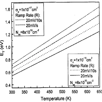
Figure 2.1 Temperature dependence of the deepest interface states that can be accurately measured. The interface state as deep as 1.57 eV can be measured at 623 K if
σp is equal to 10-17 cm2 and a very low ramp rate, 20 mV/10 s, is used [32]. ⋅⋅⋅⋅⋅⋅⋅⋅⋅⋅⋅⋅ 18
Figure 2.2 (a) Trace of gate-controlled Si MOS diode at low temperature, 79 K. First ledge is due to minority carrier injection, second is due to surface-state filling [33]. (b) Photo assisted C-V curves on a p-type 6H SiC MOS capacitor at room temperature. [34].
⋅⋅⋅⋅⋅⋅⋅⋅⋅⋅⋅⋅⋅⋅⋅⋅⋅⋅⋅⋅⋅⋅⋅⋅⋅⋅⋅⋅⋅⋅⋅⋅⋅⋅⋅⋅⋅⋅⋅⋅⋅⋅⋅⋅⋅⋅⋅⋅⋅⋅⋅⋅⋅⋅⋅⋅⋅⋅⋅⋅⋅⋅⋅⋅⋅⋅⋅⋅⋅⋅⋅⋅⋅⋅⋅⋅⋅⋅⋅⋅⋅⋅⋅⋅⋅⋅⋅⋅⋅⋅⋅⋅⋅⋅⋅⋅⋅⋅⋅⋅⋅⋅⋅⋅⋅⋅⋅⋅⋅⋅⋅⋅⋅⋅⋅⋅⋅⋅⋅⋅⋅⋅⋅⋅⋅⋅⋅⋅⋅⋅⋅⋅⋅⋅⋅⋅ 21
3. REMOTE PLASMA-ASSISTED OXIDATION OF GaN FOR LOW DEFECT DENSITY GaN-SiO2 INTERFACES
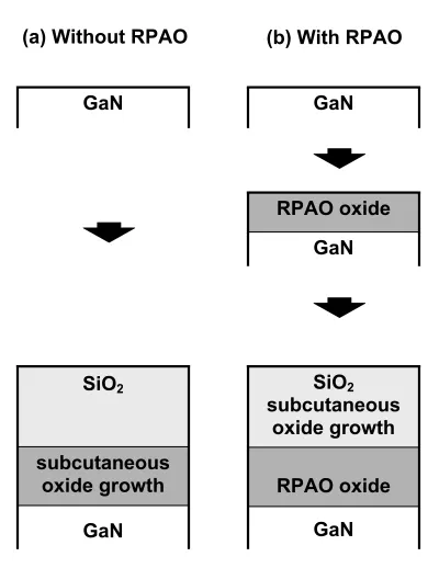
Figure 3.1 Two different process sequences were used to demonstrate the presence of subcutaneous oxidation of GaN during deposition of SiO2. (a) a direct deposition of SiO2
on GaN using RPECVD process and (b) two-step process, i.e., RPAO process to form a superficially thin RPAO oxide layer (~1.0 nm), or GaOx with x ~ 1.5 and deposition of
SiO2 on GaN using RPECVD process. ⋅⋅⋅⋅⋅⋅⋅⋅⋅⋅⋅⋅⋅⋅⋅⋅⋅⋅⋅⋅⋅⋅⋅⋅⋅⋅⋅⋅⋅⋅⋅⋅⋅⋅⋅⋅⋅⋅⋅⋅⋅⋅⋅⋅⋅⋅⋅⋅⋅⋅⋅⋅⋅⋅⋅⋅⋅⋅⋅⋅⋅⋅⋅⋅⋅⋅⋅⋅⋅⋅⋅ 43
Figure 3.2 Differential AES spectra for (i) the in situ N2/He plasma cleaned GaN
sample followed by (ii) – (vi) the SiO2 deposition on GaN sample for 20-160 s. Initial
oxide thickness (tox) prior to SiO2 film deposition on GaN sample was below 0.1 nm.
⋅⋅⋅⋅⋅⋅⋅⋅⋅⋅⋅⋅⋅⋅⋅⋅⋅⋅⋅⋅⋅⋅⋅⋅⋅⋅⋅⋅⋅⋅⋅⋅⋅⋅⋅⋅⋅⋅⋅⋅⋅⋅⋅⋅⋅⋅⋅⋅⋅⋅⋅⋅⋅⋅⋅⋅⋅⋅⋅⋅⋅⋅⋅⋅⋅⋅⋅⋅⋅⋅⋅⋅⋅⋅⋅⋅⋅⋅⋅⋅⋅⋅⋅⋅⋅⋅⋅⋅⋅⋅⋅⋅⋅⋅⋅⋅⋅⋅⋅⋅⋅⋅⋅⋅⋅⋅⋅⋅⋅⋅⋅⋅⋅⋅⋅⋅⋅⋅⋅⋅⋅⋅⋅⋅⋅⋅⋅⋅⋅⋅⋅⋅⋅⋅⋅ 44
Figure 3.3 Differential AES spectra for (i) the RPAO process of GaN sample using O2
source gas followed by (ii) – (vi) the SiO2 deposition on GaN sample for 20-160 s. Initial
oxide thickness (tox) prior to SiO2 film deposition on GaN sample was ~1.0 nm.
⋅⋅⋅⋅⋅⋅⋅⋅⋅⋅⋅⋅⋅⋅⋅⋅⋅⋅⋅⋅⋅⋅⋅⋅⋅⋅⋅⋅⋅⋅⋅⋅⋅⋅⋅⋅⋅⋅⋅⋅⋅⋅⋅⋅⋅⋅⋅⋅⋅⋅⋅⋅⋅⋅⋅⋅⋅⋅⋅⋅⋅⋅⋅⋅⋅⋅⋅⋅⋅⋅⋅⋅⋅⋅⋅⋅⋅⋅⋅⋅⋅⋅⋅⋅⋅⋅⋅⋅⋅⋅⋅⋅⋅⋅⋅⋅⋅⋅⋅⋅⋅⋅⋅⋅⋅⋅⋅⋅⋅⋅⋅⋅⋅⋅⋅⋅⋅⋅⋅⋅⋅⋅⋅⋅⋅⋅⋅⋅⋅⋅⋅⋅⋅⋅⋅⋅ 45
Figure 3.4 Comparison of determined oxide thickness (tox) of both GaN sample, shown
Figure 3.5 Peak shift of non-differentiated AES spectra by the SiO2 deposition for (ii)
20, (iii) 40, (iv) 60, (v) 80 and (vi) 180 s on GaN samples (a) without RPAO and (b) with RPAO. ⋅⋅⋅⋅⋅⋅⋅⋅⋅⋅⋅⋅⋅⋅⋅⋅⋅⋅⋅⋅⋅⋅⋅⋅⋅⋅⋅⋅⋅⋅⋅⋅⋅⋅⋅⋅⋅⋅⋅⋅⋅⋅⋅⋅⋅⋅⋅⋅⋅⋅⋅⋅⋅⋅⋅⋅⋅⋅⋅⋅⋅⋅⋅⋅⋅⋅⋅⋅⋅⋅⋅⋅⋅⋅⋅⋅⋅⋅⋅⋅⋅⋅⋅⋅⋅⋅⋅⋅⋅⋅⋅⋅⋅⋅⋅⋅⋅⋅⋅⋅⋅⋅⋅⋅⋅⋅⋅⋅⋅⋅⋅⋅⋅⋅⋅⋅⋅⋅⋅⋅⋅⋅⋅ 47
Figure 3.6 Conductance-voltage (G-V) characteristics of GaN MOS capacitors (i) without RPAO before/after PMA and (ii) with RPAO measured at room temperature and 1 MHz in the dark. ⋅⋅⋅⋅⋅⋅⋅⋅⋅⋅⋅⋅⋅⋅⋅⋅⋅⋅⋅⋅⋅⋅⋅⋅⋅⋅⋅⋅⋅⋅⋅⋅⋅⋅⋅⋅⋅⋅⋅⋅⋅⋅⋅⋅⋅⋅⋅⋅⋅⋅⋅⋅⋅⋅⋅⋅⋅⋅⋅⋅⋅⋅⋅⋅⋅⋅⋅⋅⋅⋅⋅⋅⋅⋅⋅⋅⋅⋅⋅⋅⋅⋅⋅⋅⋅⋅⋅⋅⋅⋅⋅⋅⋅⋅⋅⋅⋅⋅⋅⋅⋅⋅⋅⋅ 48
Figure 3.7 Calculated and measured C-V curve of the GaN capacitor with RPAO at room temperature and 1 MHz. Also shown is the measured conductance. ⋅⋅⋅⋅⋅⋅⋅⋅⋅⋅⋅⋅⋅⋅⋅⋅⋅ 49
Figure 3.8 1/C2 characteristics as a function of gate voltage. Net doping concentration (ND) obtained from the slope was 1.5 x 1018 cm-3 and 1.7 x 1018 cm-3. ⋅⋅⋅⋅⋅⋅⋅⋅⋅⋅⋅⋅⋅⋅⋅⋅⋅⋅⋅⋅⋅⋅⋅ 50
Figure 3.9 Distribution of the density of interface state (Dit) of GaN MOS capacitor with RPAO using Terman method. ⋅⋅⋅⋅⋅⋅⋅⋅⋅⋅⋅⋅⋅⋅⋅⋅⋅⋅⋅⋅⋅⋅⋅⋅⋅⋅⋅⋅⋅⋅⋅⋅⋅⋅⋅⋅⋅⋅⋅⋅⋅⋅⋅⋅⋅⋅⋅⋅⋅⋅⋅⋅⋅⋅⋅⋅⋅⋅⋅⋅⋅⋅⋅⋅⋅⋅⋅⋅⋅⋅⋅⋅⋅⋅⋅⋅⋅ 51
Figure 3.10 Calculated and measured C-V curve of the GaN capacitors without RPAO before/after PMA at room temperature and 1 MHz. ⋅⋅⋅⋅⋅⋅⋅⋅⋅⋅⋅⋅⋅⋅⋅⋅⋅⋅⋅⋅⋅⋅⋅⋅⋅⋅⋅⋅⋅⋅⋅⋅⋅⋅⋅⋅⋅⋅⋅⋅⋅⋅⋅⋅⋅⋅⋅⋅⋅⋅⋅ 52
Figure 3.11 Frequency dependence (1 kHz to 1 MHz) of the C-V characteristics of GaN MOS capacitors (i) without RPAO after PMA and (ii) with RPAO. ⋅⋅⋅⋅⋅⋅⋅⋅⋅⋅⋅⋅⋅⋅⋅⋅⋅⋅⋅⋅⋅⋅⋅⋅⋅⋅ 53
Figure 3.12 Density of interface state (Dit) of GaN MOS capacitors (i) without RPAO and (ii) with RPAO using high-low frequency method. The minimum Dit was determined at the gate voltage where low and high C-V curves showed the maximum capacitance difference (∆Cmax). Then, minimum Dit of (i) without and (ii) with RPAO was ~4 x 1012 cm-2eV-1 at –2.5 V and ~7 x 1011 cm-2eV-1 at –4.1 V, respectively. ⋅⋅⋅⋅⋅⋅⋅⋅⋅⋅⋅⋅⋅⋅⋅⋅⋅⋅⋅⋅⋅⋅⋅⋅⋅⋅⋅⋅ 54
Figure 3.13 Distribution of the density of interface state (Dit) of GaN MOS capacitor with RPAO using Terman method and high-low frequency method. ⋅⋅⋅⋅⋅⋅⋅⋅⋅⋅⋅⋅⋅⋅⋅⋅⋅⋅⋅⋅⋅⋅⋅⋅⋅ 55
Figure 3.14 Parallel conductance loss (Gp/ω) versus angular frequency (ω) curves measured at 25 oC for GaN MOS capacitor without RPAO after PMA. The graphically determined standard deviation of band bending (σs) was 0.5-0.9 (in the unit of kT/q). ⋅⋅⋅⋅⋅⋅⋅⋅⋅⋅⋅⋅⋅⋅⋅⋅⋅⋅⋅⋅⋅⋅⋅⋅⋅⋅⋅⋅⋅⋅⋅⋅⋅⋅⋅⋅⋅⋅⋅⋅⋅⋅⋅⋅⋅⋅⋅⋅⋅⋅⋅⋅⋅⋅⋅⋅⋅⋅⋅⋅⋅⋅⋅⋅⋅⋅⋅⋅⋅⋅⋅⋅⋅⋅⋅⋅⋅⋅⋅⋅⋅⋅⋅⋅⋅⋅⋅⋅⋅⋅⋅⋅⋅⋅⋅⋅⋅⋅⋅⋅⋅⋅⋅⋅⋅⋅⋅⋅⋅⋅⋅⋅⋅⋅⋅⋅⋅⋅⋅⋅⋅⋅⋅ 56
Figure 3.15 Parallel conductance loss (Gp/ω) versus angular frequency (ω) curves measured at 25 oC for GaN MOS capacitor with RPAO. The graphically determined standard deviation of band bending (σs) was 1.7-1.9 (in the unit of kT/q). ⋅⋅⋅⋅⋅⋅⋅⋅⋅⋅⋅⋅⋅⋅⋅⋅ 57
Figure 3.17 C-V characteristics of GaN MOS capacitors with RPAO measured at 25-200 oC in the dark. Also shown is the change in polarization charge (∆Q) by increasing temperatuere [23]. ⋅⋅⋅⋅⋅⋅⋅⋅⋅⋅⋅⋅⋅⋅⋅⋅⋅⋅⋅⋅⋅⋅⋅⋅⋅⋅⋅⋅⋅⋅⋅⋅⋅⋅⋅⋅⋅⋅⋅⋅⋅⋅⋅⋅⋅⋅⋅⋅⋅⋅⋅⋅⋅⋅⋅⋅⋅⋅⋅⋅⋅⋅⋅⋅⋅⋅⋅⋅⋅⋅⋅⋅⋅⋅⋅⋅⋅⋅⋅⋅⋅⋅⋅⋅⋅⋅⋅⋅⋅⋅⋅⋅⋅⋅⋅⋅⋅⋅⋅⋅⋅⋅⋅⋅ 59
Figure 3.18 Photo-assisted C-V characteristics of GaN MOS capacitors measured at room temperature and 1 MHz. ⋅⋅⋅⋅⋅⋅⋅⋅⋅⋅⋅⋅⋅⋅⋅⋅⋅⋅⋅⋅⋅⋅⋅⋅⋅⋅⋅⋅⋅⋅⋅⋅⋅⋅⋅⋅⋅⋅⋅⋅⋅⋅⋅⋅⋅⋅⋅⋅⋅⋅⋅⋅⋅⋅⋅⋅⋅⋅⋅⋅⋅⋅⋅⋅⋅⋅⋅⋅⋅⋅⋅⋅⋅⋅⋅⋅⋅⋅⋅⋅⋅⋅⋅⋅⋅ 60
4. REMOTE PLASMA-ASSISTED OXIDATION OF GaN AND NITROGEN INCORPORATION
Figure 4.1 Schematic representation of three samples; (a) clean GaN substrate, (b) thick pure GaOx and (c) thin pure GaOx on GaN substrate. IoN (or IN) is N KLL Auger
electron intensity from the clean GaN substrate (or from the GaN substrate with thin oxide). IoO (or IO) is O KLL Auger electron intensity from the thick GaOx layer (or from
the thin GaOx layer). ⋅⋅⋅⋅⋅⋅⋅⋅⋅⋅⋅⋅⋅⋅⋅⋅⋅⋅⋅⋅⋅⋅⋅⋅⋅⋅⋅⋅⋅⋅⋅⋅⋅⋅⋅⋅⋅⋅⋅⋅⋅⋅⋅⋅⋅⋅⋅⋅⋅⋅⋅⋅⋅⋅⋅⋅⋅⋅⋅⋅⋅⋅⋅⋅⋅⋅⋅⋅⋅⋅⋅⋅⋅⋅⋅⋅⋅⋅⋅⋅⋅⋅⋅⋅⋅⋅⋅⋅⋅⋅⋅⋅⋅⋅⋅⋅⋅⋅⋅⋅ 75
Figure 4.2 Differential AES spectra from (i) clean GaN, (ii) thick RPAO oxide and (iii) thin RPAO oxide on GaN substrate. N2/He plasma cleaned GaN sample (300
o
C, 0.02 Torr, 30 W and 15 min) was used as a reference sample for a clean GaN, and O2/He
plasma oxidized GaN sample (300 oC, 0.3 Torr, 60 W and 30 min) was used as a reference sample for a thick pure GaOx. ⋅⋅⋅⋅⋅⋅⋅⋅⋅⋅⋅⋅⋅⋅⋅⋅⋅⋅⋅⋅⋅⋅⋅⋅⋅⋅⋅⋅⋅⋅⋅⋅⋅⋅⋅⋅⋅⋅⋅⋅⋅⋅⋅⋅⋅⋅⋅⋅⋅⋅⋅⋅⋅⋅⋅⋅⋅⋅⋅⋅⋅⋅⋅⋅⋅⋅⋅⋅⋅ 76
Figure 4.3 Schematic representation of thin RPAO oxide, or GaOxNy with
non-negligible nitrogen content, on GaN substrate. When the nitrogen content in the oxide does not negligible, total intensity of N KLL (IN) consists of i) intensity of N KLL from
the substrate (IN, sub) and ii) intensity of N KLL from oxide film (IN, film).
⋅⋅⋅⋅⋅⋅⋅⋅⋅⋅⋅⋅⋅⋅⋅⋅⋅⋅⋅⋅⋅⋅⋅⋅⋅⋅⋅⋅⋅⋅⋅⋅⋅⋅⋅⋅⋅⋅⋅⋅⋅⋅⋅⋅⋅⋅⋅⋅⋅⋅⋅⋅⋅⋅⋅⋅⋅⋅⋅⋅⋅⋅⋅⋅⋅⋅⋅⋅⋅⋅⋅⋅⋅⋅⋅⋅⋅⋅⋅⋅⋅⋅⋅⋅⋅⋅⋅⋅⋅⋅⋅⋅⋅⋅⋅⋅⋅⋅⋅⋅⋅⋅⋅⋅⋅⋅⋅⋅⋅⋅⋅⋅⋅⋅⋅⋅⋅⋅⋅⋅⋅⋅⋅⋅⋅⋅⋅⋅⋅⋅⋅⋅⋅⋅⋅⋅ 77
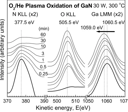
Figure 4.4 Time evolution of differential AES spectra from (i) N2/He plasma cleaned
GaN sample and (ii)-(vi) O2/He plasma oxidation processing of GaN surface for 0.5 to 30
min. ⋅⋅⋅⋅⋅⋅⋅⋅⋅⋅⋅⋅⋅⋅⋅⋅⋅⋅⋅⋅⋅⋅⋅⋅⋅⋅⋅⋅⋅⋅⋅⋅⋅⋅⋅⋅⋅⋅⋅⋅⋅⋅⋅⋅⋅⋅⋅⋅⋅⋅⋅⋅⋅⋅⋅⋅⋅⋅⋅⋅⋅⋅⋅⋅⋅⋅⋅⋅⋅⋅⋅⋅⋅⋅⋅⋅⋅⋅⋅⋅⋅⋅⋅⋅⋅⋅⋅⋅⋅⋅⋅⋅⋅⋅⋅⋅⋅⋅⋅⋅⋅⋅⋅⋅⋅⋅⋅⋅⋅⋅⋅⋅⋅⋅⋅⋅⋅⋅⋅⋅⋅⋅⋅⋅⋅⋅ 78
Figure 4.5 Log-log plots of the oxide thickness (tox) as a function of oxidation time (t)
for the RPAO process using O2 source gas at 250 and 300 oC, respectively. The straight
lines connecting the data points represent a power-law dependence, i.e., tox = τotβ, where
τo and β are fitting parameters. The oxide thickness is determined from Eq. (4.3) using
IO/IN with an assumption of a homogeneous overlayer/substrate (GaOx/GaN) system
⋅⋅⋅⋅⋅⋅⋅⋅⋅⋅⋅⋅⋅⋅⋅⋅⋅⋅⋅⋅⋅⋅⋅⋅⋅⋅⋅⋅⋅⋅⋅⋅⋅⋅⋅⋅⋅⋅⋅⋅⋅⋅⋅⋅⋅⋅⋅⋅⋅⋅⋅⋅⋅⋅⋅⋅⋅⋅⋅⋅⋅⋅⋅⋅⋅⋅⋅⋅⋅⋅⋅⋅⋅⋅⋅⋅⋅⋅⋅⋅⋅⋅⋅⋅⋅⋅⋅⋅⋅⋅⋅⋅⋅⋅⋅⋅⋅⋅⋅⋅⋅⋅⋅⋅⋅⋅⋅⋅⋅⋅⋅⋅⋅⋅⋅⋅⋅⋅⋅⋅⋅⋅⋅⋅⋅⋅⋅⋅⋅⋅⋅⋅⋅⋅⋅⋅ 79
Figure 4.6 Log-log plots of the oxide thickness (tox), determined from Eq. (4.4) using
IO/IGa and taking λΟas 1.14 nm, as a function of oxidation time (t) for the same RPAO
Figure 4.7 Time evolution of non-differential AES spectra from in-situ N2/He plasma
cleaned GaN sample and O2/He plasma oxidation processing of GaN surface for 0.25 to
60 min. ⋅⋅⋅⋅⋅⋅⋅⋅⋅⋅⋅⋅⋅⋅⋅⋅⋅⋅⋅⋅⋅⋅⋅⋅⋅⋅⋅⋅⋅⋅⋅⋅⋅⋅⋅⋅⋅⋅⋅⋅⋅⋅⋅⋅⋅⋅⋅⋅⋅⋅⋅⋅⋅⋅⋅⋅⋅⋅⋅⋅⋅⋅⋅⋅⋅⋅⋅⋅⋅⋅⋅⋅⋅⋅⋅⋅⋅⋅⋅⋅⋅⋅⋅⋅⋅⋅⋅⋅⋅⋅⋅⋅⋅⋅⋅⋅⋅⋅⋅⋅⋅⋅⋅⋅⋅⋅⋅⋅⋅⋅⋅⋅⋅⋅⋅⋅⋅⋅⋅⋅⋅ 81
Figure 4.8 Relative change in composition of oxidized GaN sample as a function of oxidation time, where, [Ga], [O] and [N] are Ga, O and N atomic fraction in the film (at. %). ⋅⋅⋅⋅⋅⋅⋅⋅⋅⋅⋅⋅⋅⋅⋅⋅⋅⋅⋅⋅⋅⋅⋅⋅⋅⋅⋅⋅⋅⋅⋅⋅⋅⋅⋅⋅⋅⋅⋅⋅⋅⋅⋅⋅⋅⋅⋅⋅⋅⋅⋅⋅⋅⋅⋅⋅⋅⋅⋅⋅⋅⋅⋅⋅⋅⋅⋅⋅⋅⋅⋅⋅⋅⋅⋅⋅⋅⋅⋅⋅⋅⋅⋅⋅⋅⋅⋅⋅⋅⋅⋅⋅⋅⋅⋅⋅⋅⋅⋅⋅⋅⋅⋅⋅⋅⋅⋅⋅⋅⋅⋅⋅⋅⋅⋅⋅⋅⋅⋅⋅⋅⋅⋅⋅⋅⋅⋅⋅ 82
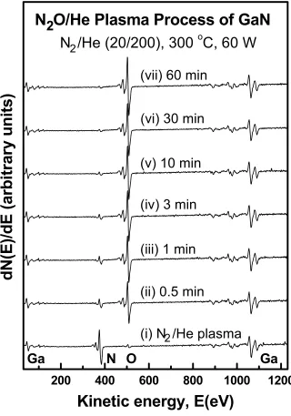
Figure 4.9 Time evolution of differential AES spectra from (i) N2/He plasma cleaned
GaN sample and (ii)-(vii) N2O/He plasma oxidation processing of GaN surface for 0.5 to
60 min. The notation (20/200) in the figure refers to the flow rates of N2O and He,
respectively, in units of standard cubic centimeters per second (sccm). ⋅⋅⋅⋅⋅⋅⋅⋅⋅⋅⋅⋅⋅⋅⋅⋅⋅⋅⋅⋅⋅ 83
Figure 4.10 Log-log plots of the oxide thickness (tox) as a function of oxidation time (t)
for the RPAO process using N2O source gas at 300 oC with 30 and 60 W, respectively.
The oxide thickness is determined from Eq. (3) using IO/IN. The oxide thickness and
fitting data using O2 source gas are also included as references. ⋅⋅⋅⋅⋅⋅⋅⋅⋅⋅⋅⋅⋅⋅⋅⋅⋅⋅⋅⋅⋅⋅⋅⋅⋅⋅⋅⋅⋅⋅⋅ 84
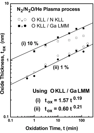
Figure 4.11 Log-log plots of the oxide thickness (tox), determined from Eq. (4) using
IO/IGa and taking λΟas 1.14 nm as a function of oxidation time (t). The notation 10 % and
1 % in the figure refer to 10 % N2O in N2 and 1 % N2O in N2. ⋅⋅⋅⋅⋅⋅⋅⋅⋅⋅⋅⋅⋅⋅⋅⋅⋅⋅⋅⋅⋅⋅⋅⋅⋅⋅⋅⋅⋅⋅⋅⋅⋅⋅ 85
Figure 4.12 Relative change in composition of oxidized GaN sample as a function of oxidation time, where, [Ga], [O] and [N] are Ga, O and N atomic fraction in the film (at. %). ⋅⋅⋅⋅⋅⋅⋅⋅⋅⋅⋅⋅⋅⋅⋅⋅⋅⋅⋅⋅⋅⋅⋅⋅⋅⋅⋅⋅⋅⋅⋅⋅⋅⋅⋅⋅⋅⋅⋅⋅⋅⋅⋅⋅⋅⋅⋅⋅⋅⋅⋅⋅⋅⋅⋅⋅⋅⋅⋅⋅⋅⋅⋅⋅⋅⋅⋅⋅⋅⋅⋅⋅⋅⋅⋅⋅⋅⋅⋅⋅⋅⋅⋅⋅⋅⋅⋅⋅⋅⋅⋅⋅⋅⋅⋅⋅⋅⋅⋅⋅⋅⋅⋅⋅⋅⋅⋅⋅⋅⋅⋅⋅⋅⋅⋅⋅⋅⋅⋅⋅⋅⋅⋅⋅⋅⋅⋅⋅ 86
Figure 4.13 Time evolution of differential AES spectra from (i) O2/He plasma oxidized
GaN sample (GaOx, ~3.5 nm) and (ii)-(vi) N2/He plasma nitridation processing of GaOx
for 5 to 150 min. ⋅⋅⋅⋅⋅⋅⋅⋅⋅⋅⋅⋅⋅⋅⋅⋅⋅⋅⋅⋅⋅⋅⋅⋅⋅⋅⋅⋅⋅⋅⋅⋅⋅⋅⋅⋅⋅⋅⋅⋅⋅⋅⋅⋅⋅⋅⋅⋅⋅⋅⋅⋅⋅⋅⋅⋅⋅⋅⋅⋅⋅⋅⋅⋅⋅⋅⋅⋅⋅⋅⋅⋅⋅⋅⋅⋅⋅⋅⋅⋅⋅⋅⋅⋅⋅⋅⋅⋅⋅⋅⋅⋅⋅⋅⋅⋅⋅⋅⋅⋅⋅⋅⋅⋅⋅⋅ 87
Figure 4.14 Time evolution of non-differential AES spectra from O2/He plasma
oxidized GaN sample (GaOx, ~3.5 nm) and N2/He plasma nitridation processing of
GaOx. ⋅⋅⋅⋅⋅⋅⋅⋅⋅⋅⋅⋅⋅⋅⋅⋅⋅⋅⋅⋅⋅⋅⋅⋅⋅⋅⋅⋅⋅⋅⋅⋅⋅⋅⋅⋅⋅⋅⋅⋅⋅⋅⋅⋅⋅⋅⋅⋅⋅⋅⋅⋅⋅⋅⋅⋅⋅⋅⋅⋅⋅⋅⋅⋅⋅⋅⋅⋅⋅⋅⋅⋅⋅⋅⋅⋅⋅⋅⋅⋅⋅⋅⋅⋅⋅⋅⋅⋅⋅⋅⋅⋅⋅⋅⋅⋅⋅⋅⋅⋅⋅⋅⋅⋅⋅⋅⋅⋅⋅⋅⋅⋅⋅⋅⋅⋅⋅⋅⋅⋅⋅⋅⋅ 88
Figure 4.15 Relative change in composition of GaOx as a function of nitridation time,
where, [Ga], [O] and [N] are Ga, O and N atomic fraction in the film (at. %). ⋅⋅⋅⋅⋅⋅⋅⋅⋅⋅ 89
Figure 4.16 Frequency dependence (3 kHz, 10 kHz, 100 kHz, and 1 MHz) of the C-V
characteristics of GaN MOS capacitors. The RPAO process using O2 source gas was
Figure 4.17 Frequency dependence (3 kHz, 10 kHz, 100 kHz, and 1 MHz) of the C-V
characteristics of GaN MOS capacitors. (a) the RPAO process using 1% N2O in N2
source gas and (b) the RPAO process using O2 source gas with followed nitridation using
N2/He plasma. The minimum Dit of each GaN MOS capacitor was determined at the gate
voltage where C-V curves measured at 3 kHz and 1 Mhz showed the maximum capacitance difference (∆Cmax). ⋅⋅⋅⋅⋅⋅⋅⋅⋅⋅⋅⋅⋅⋅⋅⋅⋅⋅⋅⋅⋅⋅⋅⋅⋅⋅⋅⋅⋅⋅⋅⋅⋅⋅⋅⋅⋅⋅⋅⋅⋅⋅⋅⋅⋅⋅⋅⋅⋅⋅⋅⋅⋅⋅⋅⋅⋅⋅⋅⋅⋅⋅⋅⋅⋅⋅⋅⋅⋅⋅⋅⋅⋅⋅⋅⋅⋅⋅⋅⋅⋅⋅⋅ 91
Figure 4.18 Minimum density of interface state (Dit) of GaN MOS capacitors with RPAO process using (i) O2 source gas for 30 s, (ii) O2 source gas for 180 s, (iii) 1% N2O
in N2 source gas for 600 s and (iv) O2 source gas for 30 s with followed nitridation using
N2/He plasma for 90 s. ⋅⋅⋅⋅⋅⋅⋅⋅⋅⋅⋅⋅⋅⋅⋅⋅⋅⋅⋅⋅⋅⋅⋅⋅⋅⋅⋅⋅⋅⋅⋅⋅⋅⋅⋅⋅⋅⋅⋅⋅⋅⋅⋅⋅⋅⋅⋅⋅⋅⋅⋅⋅⋅⋅⋅⋅⋅⋅⋅⋅⋅⋅⋅⋅⋅⋅⋅⋅⋅⋅⋅⋅⋅⋅⋅⋅⋅⋅⋅⋅⋅⋅⋅⋅⋅⋅⋅⋅⋅⋅⋅⋅⋅⋅⋅⋅⋅ 92
5. LOW TEMPERATURE REMOTE N2/He PLASMA-ASSISTED CLEANING OF GaN SURFACE
Figure 5.1 Differential AES spectra of (i) as-loaded (after etching in 1:5 NH4OH:H2O),
and N2/He plasma treated GaN surface at 300 oC for 15 min at (ii) 0.02, (iii) 0.1 and (iv)
0.3 Torr, respectively. ⋅⋅⋅⋅⋅⋅⋅⋅⋅⋅⋅⋅⋅⋅⋅⋅⋅⋅⋅⋅⋅⋅⋅⋅⋅⋅⋅⋅⋅⋅⋅⋅⋅⋅⋅⋅⋅⋅⋅⋅⋅⋅⋅⋅⋅⋅⋅⋅⋅⋅⋅⋅⋅⋅⋅⋅⋅⋅⋅⋅⋅⋅⋅⋅⋅⋅⋅⋅⋅⋅⋅⋅⋅⋅⋅⋅⋅⋅⋅⋅⋅⋅⋅⋅⋅⋅⋅⋅⋅⋅⋅⋅⋅⋅⋅⋅ 104
Figure 5.2 Differential AES spectra of GaN surface after etching in (a) 1:1 HCl:H2O
(RT), (b) 1:1 HCl:H2O (90 oC) and (c) 3:1 HCl:HNO3 (90 oC). After in situ N2/He plasma
treatment at 0.02 Torr, C and Cl were reduced below AES detection and O KLL/N KLL
reduce to ~0.06 regardless of varied wet chemical treatments. ⋅⋅⋅⋅⋅⋅⋅⋅⋅⋅⋅⋅⋅⋅⋅⋅⋅⋅⋅⋅⋅⋅⋅⋅⋅⋅⋅⋅⋅⋅⋅⋅⋅⋅⋅⋅⋅⋅⋅⋅⋅⋅⋅⋅⋅⋅⋅⋅⋅⋅⋅⋅⋅⋅⋅⋅⋅⋅⋅⋅⋅⋅⋅⋅⋅⋅⋅⋅⋅⋅⋅⋅⋅⋅⋅⋅⋅⋅⋅⋅⋅⋅⋅⋅⋅⋅⋅⋅⋅⋅⋅⋅⋅⋅⋅⋅⋅⋅⋅⋅⋅⋅⋅⋅⋅⋅⋅⋅⋅⋅⋅⋅⋅⋅ 105
Figure 5.3 Non-differential AES spectra, after subtracting inelastic background, of N2/He plasma treated GaN surface at (i) 0.02, (ii) 0.1 and (iii) 0.3 Torr, respectively.
⋅⋅⋅⋅⋅⋅⋅⋅⋅⋅⋅⋅⋅⋅⋅⋅⋅⋅⋅⋅⋅⋅⋅⋅⋅⋅⋅⋅⋅⋅⋅⋅⋅⋅⋅⋅⋅⋅⋅⋅⋅⋅⋅⋅⋅⋅⋅⋅⋅⋅⋅⋅⋅⋅⋅⋅⋅⋅⋅⋅⋅⋅⋅⋅⋅⋅⋅⋅⋅⋅⋅⋅⋅⋅⋅⋅⋅⋅⋅⋅⋅⋅⋅⋅⋅⋅⋅⋅⋅⋅⋅⋅⋅⋅⋅⋅⋅⋅⋅⋅⋅⋅⋅⋅⋅⋅⋅⋅⋅⋅⋅⋅⋅⋅⋅⋅⋅⋅⋅⋅⋅⋅⋅⋅⋅⋅⋅⋅⋅⋅⋅⋅⋅⋅ 106
Figure 5.4 Differential AES spectra of 0.02 Torr N2/He plasma treated GaN surface
followed by the He plasma exposure at 300 oC for 15 min at (i) 0.03 Torr and (ii) 0.3 Torr, respectively. ⋅⋅⋅⋅⋅⋅⋅⋅⋅⋅⋅⋅⋅⋅⋅⋅⋅⋅⋅⋅⋅⋅⋅⋅⋅⋅⋅⋅⋅⋅⋅⋅⋅⋅⋅⋅⋅⋅⋅⋅⋅⋅⋅⋅⋅⋅⋅⋅⋅⋅⋅⋅⋅⋅⋅⋅⋅⋅⋅⋅⋅⋅⋅⋅⋅⋅⋅⋅⋅⋅⋅⋅⋅⋅⋅⋅⋅⋅⋅⋅⋅⋅⋅⋅⋅⋅⋅⋅⋅⋅⋅⋅⋅⋅⋅⋅⋅⋅⋅⋅⋅⋅⋅⋅⋅⋅⋅⋅⋅⋅⋅ 108
Figure 5.5 Proposed plasma cleaning mechanism. The bond energy difference between NO+ and N2+ is 93 kcal/mol, or ~4 eV, and the bond energy difference between Ga-N and
Ga-O is thought less than ~1-2 eV. Therefore, N2+ can react with electronegative O on
GaN surface and diffuse out as gaseous molecules such as NO+ by the following reaction, N2+ + Ga-O → Ga-N + NO+. ⋅⋅⋅⋅⋅⋅⋅⋅⋅⋅⋅⋅⋅⋅⋅⋅⋅⋅⋅⋅⋅⋅⋅⋅⋅⋅⋅⋅⋅⋅⋅⋅⋅⋅⋅⋅⋅⋅⋅⋅⋅⋅⋅⋅⋅⋅⋅⋅⋅⋅⋅⋅⋅⋅⋅⋅⋅⋅⋅⋅⋅⋅⋅⋅⋅⋅⋅⋅⋅⋅⋅⋅⋅⋅⋅⋅⋅⋅⋅⋅⋅⋅⋅⋅⋅ 109
Figure 5.6 Frequency dependence of C-V characteristics of GaN MOS capacitors. SiO2
film (~35 nm) was deposited on GaN substrate after (i) wet chemical (or NH4OH:H2O)
etching of native oxide, and (ii) wet chemical (or NH4OH:H2O) etching of native oxide
Figure 5.7 Frequency dependence of C-V characteristics of GaN MOS capacitors. SiO2
film (~35 nm) was deposited on GaN substrate after wet chemical (or NH4OH:H2O2:H2O)
growing of native oxide. ⋅⋅⋅⋅⋅⋅⋅⋅⋅⋅⋅⋅⋅⋅⋅⋅⋅⋅⋅⋅⋅⋅⋅⋅⋅⋅⋅⋅⋅⋅⋅⋅⋅⋅⋅⋅⋅⋅⋅⋅⋅⋅⋅⋅⋅⋅⋅⋅⋅⋅⋅⋅⋅⋅⋅⋅⋅⋅⋅⋅⋅⋅⋅⋅⋅⋅⋅⋅⋅⋅⋅⋅⋅⋅⋅⋅⋅⋅⋅⋅⋅⋅⋅⋅⋅⋅⋅⋅⋅⋅⋅⋅ 111
Figure 5.8 Frequency dependence of C-V characteristics of GaN MOS capacitors. SiO2
film (~35 nm) was deposited on GaN substrate after in situ N2/He plasma cleaning at 0.02
Torr of wet chemical (or NH4OH:H2O) treated GaN surface and followed RPAO process
to form ~1.0 nm of the RPAO oxide. ⋅⋅⋅⋅⋅⋅⋅⋅⋅⋅⋅⋅⋅⋅⋅⋅⋅⋅⋅⋅⋅⋅⋅⋅⋅⋅⋅⋅⋅⋅⋅⋅⋅⋅⋅⋅⋅⋅⋅⋅⋅⋅⋅⋅⋅⋅⋅⋅⋅⋅⋅⋅⋅⋅⋅⋅⋅⋅⋅⋅⋅⋅⋅⋅⋅⋅⋅⋅⋅⋅⋅⋅ 112
Figure 5.9 Capacitance difference (∆C) between the capacitance measured at 3 kHz and the capacitance measured at 1 MHz. ⋅⋅⋅⋅⋅⋅⋅⋅⋅⋅⋅⋅⋅⋅⋅⋅⋅⋅⋅⋅⋅⋅⋅⋅⋅⋅⋅⋅⋅⋅⋅⋅⋅⋅⋅⋅⋅⋅⋅⋅⋅⋅⋅⋅⋅⋅⋅⋅⋅⋅⋅⋅⋅⋅⋅⋅⋅⋅⋅⋅⋅⋅⋅⋅⋅⋅ 113
Figure 5.10 Distribution of Dit as a function of gate voltage. The determined minimum
Dit of each GaN MOS capacitor of (i) subcutaneous oxide (at –2.5 V), (ii) RPAO oxide (at –4.1 V), (iii) wet oxide (at –3.2) and (iv) in situ cleaning and RPAO oxide (at –5.0 V) was ~4 x 10¹², ~7 x 10¹¹, ~1 x 10¹², and ~2 x 1012 cm-2eV-1, respectively. The energy
levels for these minimum Dit were located at ~0.3 eV below conduction band edge.
⋅⋅⋅⋅⋅⋅⋅⋅⋅⋅⋅⋅⋅⋅⋅⋅⋅⋅⋅⋅⋅⋅⋅⋅⋅⋅⋅⋅⋅⋅⋅⋅⋅⋅⋅⋅⋅⋅⋅⋅⋅⋅⋅⋅⋅⋅⋅⋅⋅⋅⋅⋅⋅⋅⋅⋅⋅⋅⋅⋅⋅⋅⋅⋅⋅⋅⋅⋅⋅⋅⋅⋅⋅⋅⋅⋅⋅⋅⋅⋅⋅⋅⋅⋅⋅⋅⋅⋅⋅⋅⋅⋅⋅⋅⋅⋅⋅⋅⋅⋅⋅⋅⋅⋅⋅⋅⋅⋅⋅⋅⋅⋅⋅⋅⋅⋅⋅⋅⋅⋅⋅⋅⋅⋅⋅⋅⋅⋅⋅⋅⋅⋅⋅⋅ 114
Figure 5.11 When the 0.02 Torr N2/He plasma treated GaN / RPAO / SiO2 (~30 nm)
sample was annealed at 900 oC for 30 min, the frequency dependence of C-V
characteristics was reduced. The determined minimum Dit was ~9 x 1011 cm-2eV-1 at –3.9 V. ⋅⋅⋅⋅⋅⋅⋅⋅⋅⋅⋅⋅⋅⋅⋅⋅⋅⋅⋅⋅⋅⋅⋅⋅⋅⋅⋅⋅⋅⋅⋅⋅⋅⋅⋅⋅⋅⋅⋅⋅⋅⋅⋅⋅⋅⋅⋅⋅⋅⋅⋅⋅⋅⋅⋅⋅⋅⋅⋅⋅⋅⋅⋅⋅⋅⋅⋅⋅⋅⋅⋅⋅⋅⋅⋅⋅⋅⋅⋅⋅⋅⋅⋅⋅⋅⋅⋅⋅⋅⋅⋅⋅⋅⋅⋅⋅⋅⋅⋅⋅⋅⋅⋅⋅⋅⋅⋅⋅⋅⋅⋅⋅⋅⋅⋅⋅⋅⋅⋅⋅⋅⋅⋅⋅⋅⋅ 115
6. INTERFACE PROPERTIES OF n-GaN/SiO2 MOS STRUCTURE WITH REMOTE PLASMA-ASSISTED OXIDATION AND NITRIDATION
Figure 6.1 Calculated and measured C-V curve of the GaN capacitor with remote plasma oxidation and nitridation. The C-V curve was measured at 1 MHz and 25 oC in the dark. Also shown is the measured conductance. ⋅⋅⋅⋅⋅⋅⋅⋅⋅⋅⋅⋅⋅⋅⋅⋅⋅⋅⋅⋅⋅⋅⋅⋅⋅⋅⋅⋅⋅⋅⋅⋅⋅⋅⋅⋅⋅⋅⋅⋅⋅⋅⋅⋅⋅⋅⋅⋅⋅⋅⋅⋅⋅⋅⋅ 129
Figure 6.2 1/C2 characteristics as a function of gate voltage. Net doping concentration (ND) obtained from the slope was 4.0 x 1017 cm-3. ⋅⋅⋅⋅⋅⋅⋅⋅⋅⋅⋅⋅⋅⋅⋅⋅⋅⋅⋅⋅⋅⋅⋅⋅⋅⋅⋅⋅⋅⋅⋅⋅⋅⋅⋅⋅⋅⋅⋅⋅⋅⋅⋅⋅⋅⋅⋅⋅⋅⋅⋅⋅ 130
Figure 6.3 Hysteresis of C-V curves as the gate voltage was varied from +3 to –15 V and then back to +3 V. The small hysteresis of 0.1 V was reduced to negligible value at -5 V in the retrace. ⋅⋅⋅⋅⋅⋅⋅⋅⋅⋅⋅⋅⋅⋅⋅⋅⋅⋅⋅⋅⋅⋅⋅⋅⋅⋅⋅⋅⋅⋅⋅⋅⋅⋅⋅⋅⋅⋅⋅⋅⋅⋅⋅⋅⋅⋅⋅⋅⋅⋅⋅⋅⋅⋅⋅⋅⋅⋅⋅⋅⋅⋅⋅⋅⋅⋅⋅⋅⋅⋅⋅⋅⋅⋅⋅⋅⋅⋅⋅⋅⋅⋅⋅⋅⋅⋅⋅⋅⋅⋅⋅⋅⋅⋅⋅⋅⋅⋅⋅⋅⋅⋅ 131
Figure 6.4 Frequency dependence (1 kHz, 3 kHz, 10 kHz, 100 kHz and 1 MHz) of the
C-V characteristics measured at 25 oC in the dark. ⋅⋅⋅⋅⋅⋅⋅⋅⋅⋅⋅⋅⋅⋅⋅⋅⋅⋅⋅⋅⋅⋅⋅⋅⋅⋅⋅⋅⋅⋅⋅⋅⋅⋅⋅⋅⋅⋅⋅⋅⋅⋅⋅⋅⋅⋅⋅⋅⋅⋅⋅⋅ 132
at –3.7 V. The inset shows the distribution of Dit as a function of energy from conduction band edge. ⋅⋅⋅⋅⋅⋅⋅⋅⋅⋅⋅⋅⋅⋅⋅⋅⋅⋅⋅⋅⋅⋅⋅⋅⋅⋅⋅⋅⋅⋅⋅⋅⋅⋅⋅⋅⋅⋅⋅⋅⋅⋅⋅⋅⋅⋅⋅⋅⋅⋅⋅⋅⋅⋅⋅⋅⋅⋅⋅⋅⋅⋅⋅⋅⋅⋅⋅⋅⋅⋅⋅⋅⋅⋅⋅⋅⋅⋅⋅⋅⋅⋅⋅⋅⋅⋅⋅⋅⋅⋅⋅⋅⋅⋅⋅⋅⋅⋅⋅⋅⋅⋅⋅⋅⋅⋅⋅⋅⋅⋅⋅⋅⋅⋅ 133
Figure 6.6 Parallel conductance loss (Gp/ω) versus angular frequency (ω) curves measured at 25 oC. The graphically determined standard deviation of band bending (σs)
was ~1.5-2.4 (in the unit of kT/q). ⋅⋅⋅⋅⋅⋅⋅⋅⋅⋅⋅⋅⋅⋅⋅⋅⋅⋅⋅⋅⋅⋅⋅⋅⋅⋅⋅⋅⋅⋅⋅⋅⋅⋅⋅⋅⋅⋅⋅⋅⋅⋅⋅⋅⋅⋅⋅⋅⋅⋅⋅⋅⋅⋅⋅⋅⋅⋅⋅⋅⋅⋅⋅⋅⋅⋅⋅⋅⋅⋅⋅⋅⋅⋅⋅⋅⋅ 134
Figure 6.7 Density of interface state (Dit) using conductance method and high-low frequency method. ⋅⋅⋅⋅⋅⋅⋅⋅⋅⋅⋅⋅⋅⋅⋅⋅⋅⋅⋅⋅⋅⋅⋅⋅⋅⋅⋅⋅⋅⋅⋅⋅⋅⋅⋅⋅⋅⋅⋅⋅⋅⋅⋅⋅⋅⋅⋅⋅⋅⋅⋅⋅⋅⋅⋅⋅⋅⋅⋅⋅⋅⋅⋅⋅⋅⋅⋅⋅⋅⋅⋅⋅⋅⋅⋅⋅⋅⋅⋅⋅⋅⋅⋅⋅⋅⋅⋅⋅⋅⋅⋅⋅⋅⋅⋅⋅⋅⋅⋅⋅⋅ 135
Figure 6.8 Frequency dependence (1 kHz, 3 kHz, 10 kHz, 100 kHz and 1 MHz) of the
C-V characteristics after PMA performed at 400 oC for 30 min in forming gas (N2/H2).
There are no significant changes in ND and Dit except –0.5 V shift in Vfb. ⋅⋅⋅⋅⋅⋅⋅⋅⋅⋅⋅⋅⋅⋅⋅ 136
Figure 6.9 Shift of C-V curves toward positive voltage and increased hysteresis window with increasing bias range from +5/-15 to +20/-20 V. ⋅⋅⋅⋅⋅⋅⋅⋅⋅⋅⋅⋅⋅⋅⋅⋅⋅⋅⋅⋅⋅⋅⋅⋅⋅⋅⋅⋅⋅⋅⋅⋅ 137
Figure 6.10 C-V characteristics measured at 25-300 oC in the dark. Also shown is the change in polarization charge (∆Q) by increasing temperatuere [15]. ⋅⋅⋅⋅⋅⋅⋅⋅⋅⋅⋅⋅⋅⋅⋅⋅⋅⋅⋅⋅⋅⋅ 138
Figure 6.11 Hysteresis in C-V traces with increasing temperatuere. ⋅⋅⋅⋅⋅⋅⋅⋅⋅⋅⋅⋅⋅⋅⋅⋅⋅⋅⋅⋅⋅⋅⋅ 139
Figure 6.12 Photo-assisted C-V characteristics measured at room temperature and 1 MHz. From ND of ~4.0 x 1017 cm-3, the threshold voltage (Vth) was determined as about -12 V. While the bias remained at –15 V, the sample was illuminated by ultraviolet lamp (365 nm) until the measured capacitance saturated. ⋅⋅⋅⋅⋅⋅⋅⋅⋅⋅⋅⋅⋅⋅⋅⋅⋅⋅⋅⋅⋅⋅⋅⋅⋅⋅⋅⋅⋅⋅⋅⋅⋅⋅⋅⋅⋅⋅⋅⋅⋅⋅⋅⋅⋅⋅⋅⋅⋅⋅ 140
Figure 6.13 Photo-assisted C-V characteristics where the GaN MOS sample was illuminated at –15 V until the measured capacitance arrived at the expected inversion capacitance (~19.5 pF). ⋅⋅⋅⋅⋅⋅⋅⋅⋅⋅⋅⋅⋅⋅⋅⋅⋅⋅⋅⋅⋅⋅⋅⋅⋅⋅⋅⋅⋅⋅⋅⋅⋅⋅⋅⋅⋅⋅⋅⋅⋅⋅⋅⋅⋅⋅⋅⋅⋅⋅⋅⋅⋅⋅⋅⋅⋅⋅⋅⋅⋅⋅⋅⋅⋅⋅⋅⋅⋅⋅⋅⋅⋅⋅⋅⋅⋅⋅⋅⋅⋅⋅⋅⋅⋅⋅⋅⋅⋅⋅⋅⋅⋅⋅ 141
Figure 6.14 Photo-assisted C-V characteristics of GaN MOS capacitors shown in CHAPTER THREE. ND was ~1.0 x 1018 cm-3, and Dit determined at ∆Cmax was ~7 x 1011 cm-2eV-1. During the retrace sweep after the sample was illuminated at deep depletion (i) until the measured capacitance saturated and (ii) until the measured capacitance arrived at the expected inversion capacitance. ⋅⋅⋅⋅⋅⋅⋅⋅⋅⋅⋅⋅⋅⋅⋅⋅⋅⋅⋅⋅⋅⋅⋅⋅⋅⋅⋅⋅⋅⋅⋅⋅⋅⋅⋅⋅⋅⋅⋅⋅⋅⋅⋅⋅⋅⋅⋅⋅⋅⋅⋅⋅⋅⋅⋅⋅⋅⋅⋅⋅⋅⋅⋅⋅⋅⋅⋅⋅⋅⋅⋅⋅⋅⋅⋅ 142
APPENDICES
Figure A.1 (a) Comparison of the C-V behavior measured at 10 kHz as the gate voltage is swept at 100 mV/s from +5 to –12 V and then back to +5 V with the theoretical C-V
Figure B.1 Equivalent circuit of the MOS capacitor in depletion (a) for a single-level interface traps, (b) for a distribution of single-level interface traps. CT is the trap capacitance and Gn is the capture conductance by electron. Cit (ω) and Gp (ω) are equivalent parallel interface trap capacitance and conductance, respectively. (c) The approximate equivalent circuit of the MOS capacitor with small-scale interfacial charge non-uniformities. Cs(vs) is the capacitance per unit area corresponding to the band bending for the average interface charge density, and < is the interface trap admittance per unit area corresponding to the average band bending [1]. ⋅⋅⋅⋅⋅⋅⋅⋅⋅⋅⋅⋅⋅⋅⋅⋅ 155
> it
Y
Figure B.2 All curves have the same Dit of 1 x 1011 cm-2 eV-1. (a) A; Plot of (B.2) for a
single-level interface trap. B; Plot of (B.6) for an interface trap level continuum of constant density and capture probability. C; Plot of Gp /ω versus log ωτn corresponding to
a measured curve illustrating the observed interface trap time constant dispersion. All curves corresponding to the same interface trap density of 1 x 1011 cm-2ev-1. After Nicollian and Goetzberger [1]. (b) Plot of (B.11) with different values of the standard deviation of band bending, σS. ⋅⋅⋅⋅⋅⋅⋅⋅⋅⋅⋅⋅⋅⋅⋅⋅⋅⋅⋅⋅⋅⋅⋅⋅⋅⋅⋅⋅⋅⋅⋅⋅⋅⋅⋅⋅⋅⋅⋅⋅⋅⋅⋅⋅⋅⋅⋅⋅⋅⋅⋅⋅⋅⋅⋅⋅⋅⋅⋅⋅⋅⋅⋅⋅⋅⋅⋅⋅⋅⋅⋅⋅⋅⋅⋅⋅⋅⋅⋅⋅⋅ 156 Figure B.3 After Nicollian et al [1]. Each equation is solved numerically with
05 . 0
=
∆σs and ∆ξp=0.001, and redrawn. (a) Plot of ξp as a function of σs from
(B.16). (b) Plot of Gp /ω versus frequency. fp is the frequency corresponding to the peak
value of Gp /ω. The points at 1/5 fp and 5 fp define the width of the curve on the low and
high frequency side of fp, respectively. (c) Plot of
(
) (
)
p
f
ω p n p
f
p G
G /ω / / / and
(
p) (
nfp p)
fpG
G /ω / /ω as the single-valued functions of σs(choosing n = 5) calculated from
(B.11). (d) Plot of fD(σs) as a function of σs from (B.19). ⋅⋅⋅⋅⋅⋅⋅⋅⋅⋅⋅⋅⋅⋅⋅⋅⋅⋅⋅⋅⋅⋅⋅⋅⋅⋅⋅⋅⋅⋅⋅⋅⋅⋅⋅⋅ 157 Figure B.4 Conductance loss versus frequency of Si MOS capacitors of (a) an Si/RPAO/SiO2 on p-type Si substrate with Al gate, before PMA, and (b) thermal oxide of p-type Si substrate with P+-poly gate, after PMA. Peak points from system noise at specific frequency were masked before Gaussian fitting. If capacitors with large area (>3002µm2) and thick oxide (>10 nm) are used, the values of D
it up to 1 x 1011 cm-2eV-1
or less (equal to the conductance loss of ~10 pF) will be easily determined. ⋅⋅⋅⋅⋅⋅⋅⋅⋅⋅⋅⋅ 158
CHAPTER ONE
INTRODUCTION
1.1 INTRODUCTION
For the last 40 years, the miniaturization of metal-oxide-semiconductor (MOS)
field effect transistors (FET) has been successfully accomplished based on the unique
features of Si-SiO2 system. There have been innumerous researches to obtain another gate
dielectric insulator comparable to the thermally grown SiO2, but the superior position of
Si-SiO2 system in the MOS technology has never been replaced. Currently, however,
alternative gate dielectric insulators with high dielectric constants are urgently seeking
because the aggressive scaling of Si MOSFET limits the use of SiO2 as a gate dielectric
insulator. The elaborated researches for alternative gate dielectrics of Si MOS technology
have been extending basic understandings of semiconductor-dielectric insulator interface.
These understandings also can be applied to semiconductors other than Si that cannot
realize acceptable MOSFET due to the lack of a stable semiconductor-insulator interface.
The objective of this research is the extension of remote plasma processing [1-8],
including oxidation, nitridation, oxide and nitride depositions, to the formation of
GaN-dielectric insulator interface with low interface state density (Dit).
1.1.1 Remote plasma processing for gate dielectric insulators
Our group has extensively investigated the application of remote plasma
processing, which offers wide process windows for oxidation, nitridation, and oxide,
oxinitride and nitride film deposition [1-4]. A subcutaneous oxidation process, which
assisted deposition of an SiO2 film [1]. The presence of a poor quality, highly strained
subcutaneous oxide could lead to degraded device performance. To prepare device
quality Si-SiO2 interface and dielectric bulk film (SiO2), the superficially thin oxide layer
(~0.6 nm) is formed on silicon substrate by a remote plasma-assisted oxidation (RPAO)
process, and the remainder of the oxide layer is deposited by a remote plasma enhanced
chemical vapor deposition (RPECVD) process [2-4]. The RPAO process also provides an
in situ surface cleaning by removing residual levels of carbon and fluorine interface
contaminants from otherwise hydrogen terminated Si surface. This independent control
of interface formation and dielectric bulk film deposition has been also successfully
applied to the incorporation of nitrogen atoms, and nitride-oxide (ONO) or
oxide-nitride (ON) composite structures. For these cases, the RPAO process has one more key
role in the reduced net oxide charges, which was explained by extending constraint
theory [4]. The Si-SiO2 interface nitridation is demonstrated by i) an RPAO process that
uses excited species from a remote N2O/He plasma and ii) a post-RPAO process that uses
two separate interface formation steps: RPAO process by O2/He plasma and followed
remotely activated N2/He plasma nitridation step. From the consideration of chemical
bonding constraints, the substitution of alternative high-k gate dielectrics of SiO2 possibly
needs an interfacial SiO2 or nitrided SiO2 buffer layers [5]. The same RPAO-RPECVD
process has been applied to SiC [6], Ge [7], and GaN [8] and yielded
semiconductor-dielectric interface with reduced net oxide charges compared with the direct deposition of
SiO2 film on semiconductor substrate.
The growth of native oxide on the III-V semiconductors is far more complex than
on Si because one element may diffuse, evaporate, or dissolve faster than the other. Thus,
the chemical composition of bulk oxide layer or its interface may be highly nonuniform.
It is not readily apparent whether a thin native oxide is desirable or not for insulator/III-V
semiconductors. Most of the research indicates that native oxides do more harm than
good. The oxides of the column V elements, As2O3, Sb2O3, and P2O5 are volatile, and
some oxides are water-soluble. Preferential evaporation of column V element can create
vacancy defects and leave a metallic residue. The initial oxide may be the source of oxide
traps which could cause Fermi-level pinning and electrical interface instabilities (charge
injection into the interface) [9].
For n-type GaN metal-insulator-semiconductor (MIS) systems, interface state
densities (Dit) in the range of low-to-mid 1011 cm-2eV-1 have been obtained without in-situ
native oxide removal and thin intermediate layer (or sacrificial layer) preparation [10].
These results are remarkably different from the other compound semiconductors where
surface passivation has been an important issue to avoid thin native oxide formation. The
main difference of GaN from other III-V semiconductors, such as GaAs and GaP, is the
volatility of N oxide species, e.g., NO, N2O, etc. This suggests that a thin native oxide of
GaN prepared by RPAO process can be used to control semiconductor-deposited
dielectrics interface.
1.1.3 GaN-dielectric insulator interface for gate dielectrics/passivation
The intrinsic carrier density (ni) of a semiconductor is given by [11]
(
)
E kT dedh i
g
e m m h
kT
n 3/4 /2
2 / 3 2
2
2 −
where k and h are Boltzmann’s and Plank’s constants, T is the absolute temperature, mde
and mdh are the electron and hole density of state effective masses, and Eg is the bandgap.
Since intrinsic carrier density depends on temperature and the bandgap energy of the
semiconductor, the intrinsic carrier density of wide bandgap semiconductors exceed the
dopant density at higher temperature compared to conventional semiconductors. Wide
bandgap power devices can operate with less cooling and fewer high cost processing
steps associated with complicated structures designed to maximize heat extraction.
Conventional application limits for semiconductor devices have been –55 to 125 oC.
Temperature usually refers to the environment (air or heat sink) of the electronic devices.
Si (or silicon-on-insulator) will be used up to ~ 300 oC for signal-processing (low-power)
applications. For high power application, where junction temperature rises above
environment, the wide bandgap materials are promising. High temperature (>150 oC)
electronics are especially needed for applications, such as data gathering instrumentation
for oil/gas well, engine control system in automobiles/aircraft, and dense phase arrays for
radar [12]. Wurtzite GaN (hexagonal, α−phase) has a direct bandgap energy of 3.4 eV. GaN based FETs are promising devices for high temperatures and high power
applications, due to lower thermal generation rates and higher breakdown fields inherent
in wide-bandgap materials.
The GaN MISFETs with a gate dielectric insulator would provide lower gate
leakage current and reduce power consumption. To fabricate GaN MISFETs, it is a
primary requirement to find GaN-dielectric insulator interface with a low interface defect
density for a stable threshold and transconductance as well as a high mobility and charge
still not possible to grow a high-quality thermal oxide on GaN. The in-situ deposition of
lattice-matched heterojunctions with other group III-nitride materials, including AlN or
AlGaN, could support a GaN-based MIS technology. Another approach is to deposit
dielectric insulators that have a good interface quality. Deposited SiO2 and Al2O3 have
been the two most promising insulators for III-V semiconductor, mainly because of their
wide band gaps. Although Si3N4 is the other choice when the substrate oxidation should
be avoided completely, Si3N4 appears to be a worse candidate for the application to wide
band gap semiconductor due to small band offset and several trap levels in the lower half
of the band gap.
For GaN based hetero-structure FET (HFET) in applications requiring high power
at microwave frequencies, a significant frequency-dependent slump or even collapse in
drain current has been the major obstacle in the development of reliable high power
devices. Green et al. attribute this frequency dependent current degradation in
AlGaN/GaN high electron mobility transistors (HEMT’s) to the presence of slow-acting
trapping states between gate and drain of the device [13]. The cause of current collapse is
a charging up of a second virtual gate, physically located in the gate drain access region.
Due to the large bias voltages present on the device during a microwave power
measurement, surface states in the vicinity of the gate trap electrons, thus acting as a
negatively charged virtual gate [14]. Passivated devices using Si3N4 layers show almost
no current collapse, thus demonstrating that proper surface passivation prevents the
formation of the virtual gate [13,14].
1.2.1 Apparatus [3,4]
The implementation of remote plasma processing chambers into multichamber
cluster systems has made it possible to interrupt plasma assisted oxidation, nitridation,
and/or film deposition and then, without removing the sample from an ultrahigh vacuum
(UHV) compatible environment, perform on-line chemical analysis by Auger electron
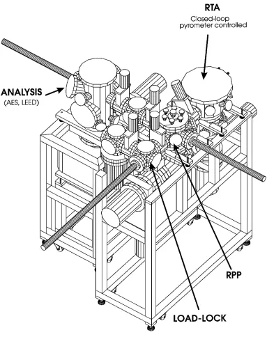
spectroscopy (AES). Figure 1.1 illustrates a top view of UHV multichamber system. This
research-level cluster tool consists of five chambers: i) a load-lock chamber for sample
introduction, ii) a remote plasma processing chamber (RPP) for (a) interface and/or top
surface oxidation/nitridation and (b) film depositions, iii) a rapid thermal annealing
(RTA) chamber for a post-oxide deposition anneal, iv) a surface analysis chamber with
AES and v) a buffer chamber for wafer transfer between analysis chamber and remote
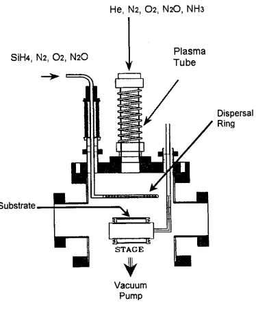
plasma processing chamber. Figure 1.2 shows a cross sectional view of the remote
plasma processing chamber. The system configuration includes three components: i) a
quartz tube which connects to an RF generator to produce localized plasma, ii) two gas
dispersal rings and iii) a heater stage to heat the wafer to temperatures up to 300 oC. The
wafer is isolated from the plasma excitation region and grounded.
The main differences for remote plasma processing from conventional or direct
plasma processing are that i) source and carrier gases are selectively excited and ii)
deposition substrate is outside of the plasma glow region. The advantages for the remote
plasma processing are i) low temperature process, ii) low plasma damage and iii)
restricted or controlled chemical pathways. In RPECVD, a high density of reactant
species is created by impact ionization in the plasma region of the reactor structure. One
diluted with He, are directly injected into the plasma tube, or upstream, except SiH4 used
for deposition of oxides, nitrides and oxynitrides. The downstream SiH4 injection
prevents SiH4 fragmentation into SiHx species, which are precursors to uncontrolled
hydrogen incorporation in the deposited dielectric films. The substrate is neutral with
respect to the plasma and is located outside of the plasma generation region. This
prevents plasma damage to the wafer surface and the deposited film from ion
bombardment generated by the plasma.
1.2.2 Two (or multi)-step process [1-8]
In this present work, the same RPAO-RPECVD process and nitridation process
have been applied to GaN. The candidates for the gate insulator of GaN MIS devices are
restricted to the SiO2 and Si3N4.
1.3 OVERVIEW OF DISSERTATION
Following this introduction, CHAPTER TWO gives (i) review of n-GaN MIS
capacitors and transistors, (ii) limitation of high frequency capacitance-voltage (C-V)
method at room temperature for wide bandgap MIS systems, and (iii) proper MIS
analysis in wide bandgap semiconductor.
CHAPTER THREE describes the two-step (or RPAO-RPECVD) process of GaN
for low defect density GaN-SiO2 interfaces. The occurrence of subcutaneous oxidation of
GaN during plasma-enhanced deposition of SiO2 films has been demonstrated by on-line
AES analysis. The quality of interface and dielectric layer with/without RPAO process
CHAPTER FOUR gives a study of the oxide growth or RPAO process via O2/He,
N2O/He, and 10 % (or 1 %) N2O in N2/He plasma processes. Two aspects of this
research are the use of on-line AES features associated with Ga, N, and O to monitor (i)
the kinetics of the oxidation processes with respect to RPAO source gas, substrate
temperature and RF plasma power and (ii) chemical composition of thin RPAO oxide and
nitrogen incorporation at interface (and/or in oxide). Using the fabricated GaN MOS
capacitors, the effect of RPAO oxide thickness and incorporated nitrogen content in
RPAO oxide on the interface state density also have been investigated.
CHAPTER FIVE presents the low temperature or 300 oC remote plasma-assisted
cleaning of GaN surface. With decreasing processing pressure of N2/He plasma, the
plasma-induced damage on GaN surface is observed.
CHAPTER SIX presents interface properties of n-GaN/SiO2 capacitors with
remote plasma-assisted oxidation and nitridation. Also, high temperature and
photo-assisted C-V characteristics are discussed.
CHAPTER SEVEN summarizes this research and provides direction for future
work.
Finally, appendices are also included in this dissertation.
1.4 REFERENCES
[1] G. G. Fountain, S. V. Hattangady, R. A. Rudder, R. J. Markunas, G. Lucovsky, S. S. Kim, and D. V. Tsu, “ Evidence for the occurrence of subcutaneous oxidation during low temperature remote plasma enhanced deposition of silicon dioxide films”, J. Vac. Sci. Technol. B 7, 576 (1989).
[2] T. Yasuda, Y. Ma, S. Habermehl, and G. Lucovsky, “Low-temperature preparation of SiO2/Si(100) interfaces using a two-step remote plasma-assisted oxidation-deposition
[3] S. V. Hattangady, H. Niimi, and G. Lucovsky, “Integrated processing of silicon oxynitride films by combined plasma and rapid-thermal processing”, J. Vac. Sci. Technol. A 14, 3017 (1996).
[4] G. Lucovsky, “Ultra thin nitrided gate dielectrics: Plasma processing, chemical characterization, Performance and reliability”, low temperature remote plasma enhanced deposition of silicon dioxide films” IBM J. Res. Develop. 43, 301 (1999).
[5] G. Lucovsky, J. C. Philips, “Limitations fro aggressively scaled CMOS Si devices due to bond coordination constants and reduced band offset energies at Si-high-k dielectric interfaces”, Appl. Surf. Sci. 166, 497 (2000).
[6] A. Gölz, G. Lucovsky, K. Koh, D. Wolfe, H. Niimi, and H. Kurz, “Plasma-assisted formation of low defect density SiC-SiO2 interfaces”, J. Vac. Sci. Technol. B 15, 1097
(1997).
[7] R. S. Johnson, H. Niimi, and G. Lucovsky, “New approach for the fabrication of device-quality Ge/GeO2/SiO2 interfaces using low temperature remote plasma
processing”, J. Vac. Sci. Technol. A 18, 1230 (2000).
[8] R. Therrien, G. Lucovsky, and R. Davis, “Charge redistribution at GaN-Ga2O3
interfaces: a microscopic mechanism for low defect density interfaces in remote-plasma-processed MOS devices prepared on polar GaN faces”, Appl. Surf. Sci.166, 513 (2000).
[9] F. Wager and C. W. Wilmsen, in Physics and Chemistry of III-V Compound Semiconductor Interfaces, edited by C. W. Wilmsen (Plenum, New York, 1985), p.165.
[10] S. J. Pearton, F. Ren, A. P. Zhang, and K. P. Lee, “Fabrication and performance of GaN electronic devices”, Mater. Sci. Eng. R 30, 55 (2000).
[11] S. M. Sze, Physics of semiconductor Devices (Wiley, New York, 1981), p. 19.
[12] R. K. Kirschman, High temperature electronics (IEEE Press, New York, 1999), p. 3.
[13] B. M. Green, K. K. Chu, E. M. Chumbes, J. A. Smart, J. A. Smart, J. R. Shealy, and L. F. Eastman, “The effect of surface passivation on the microwave characteristics of undoped AlGaN/GaN HEMT’s”, IEEE Electron Device Lett.21, 268 (2000).