Abstract
CHEN, BEI. Metal alloys and Gate Stack Engineering for CMOS Gate Electrode Application. (Under the direction of Dr. Veena Misra.)
The purpose of this research has been to search for proper metallic gate electrodes for CMOS devices. This dissertation covers several binary alloy metal gate research topics. First, intermetallic binary alloy RuY was investigated. From C-V analysis we obtained the effective work function of Ru-Y thin films to range from 5.0eV to 3.9eV which is suitable for dual metal gate CMOS. The rich Y film was found to be not stable on SiO2 dielectrics because of the high oxygen affinity of Y. RuxYy thin film may still be a candidate for low temperature process, especially due to its large range of work function. More over, RuY has smaller grain size than Ru which demonstrates one of the advantages of alloy by reducing grain size to achieve more uniform gate film and more uniform effective work function for the nano-size device applications.
Chapter 3 presents MoxTay as a potential candidate for dual metal CMOS
diffusion into substrate Si channel was detected. This indicates that MoxTay is a good candidate for CMOS metal gate applications.
Chapter 4 evaluates Ru and W capping layer for MoTa metal gate electrodes in Metal Oxide Semiconductor capacitor applications. We report that the oxygen diffusion from the capping layer plays an important role in determining the MoTa alloy effective work function value on SiO2. MoTa alloy metal gate with Ru capping exhibit stable effective work function up to 900°C anneal but is not stable with W capping. Auger electron spectroscopy and Rutherford backscattering spectroscopy analysis shows minimal oxygen diffusion into the MoTa gate stacks with Ru capping while severe oxygen diffusion into the gate is observed with W capping metal after 900°C anneal.
In chapter 5, We have studied the Φm behavior of AlTa alloys with varying compositions ranging from pure Al to pure Ta. The effective work function of AlTa alloy increased up to 4.45 eV as compared to pure Al work function (~4.1eV) or pure Ta work function (~4.2eV) on SiO2 at 400°C FGA. We ascribe the Φm increase due to an interface dipole originating froma thin negative charged reaction layer formed between the AlTa alloy and dielectric layer. In order to further increase the stability of the AlTa alloy while still obtaining Φm tuning, N was added to make AlTaN. These alloy electrodes resulted in effective work function values of ~5.13 eV after a 1000°C anneal making them suitable candidates for PMOS electrodes.
Metal Alloys and Gate Stack Engineering for CMOS Gate
Electrode Applications
by
BEI CHEN
A dissertation submitted to the Graduate Faculty of North Carolina State University
In partial fulfillment of the Requirements for the Degree of
Doctor of Philosophy
ELECTRICAL ENGINEERING
Raleigh, NC
2006
APPROVED BY:
______________________________ Dr. Veena Misra
Chair of Advisory Committee
______________________________ ______________________________ Dr. C.M. Osburn Dr. Doug W. Barlage
Biography
Acknowledgments
First of all, I wish to sincerely thank Dr. Veena Misra, for her invaluable guidance, encouragement and support in the past few years. I would like to express my sincere appreciation to my other committee members, Dr. C. M. Osburn, Dr. D. W. Barlage, and Dr. M. Johnson.
I would like to acknowledge current and former members in Dr. Misra’s group: Jaehoon Lee, Rashmi Jha, Dr. Nivedita Biswas, Bongmook Lee, Steven Novak, Srivardhan Gowda, Yong Luo, Zhong Chen, Dr. Smita Sarkar, Yan Du, Gregory Mulholland, Halit Hakan Efe, and Dr. Huicai Zhong, Dr. Greg Heuss, Dr. Youseok Suh, Dr. Heather Lazar, Dr.Yanxia Lin, Dr.Guru Mathur, Dr. Kingsuk Mathur, Dr. Qiliang Li, Dr. Qian Zhao, Dr. Shyam Surthi, Jason Gurganos, Mais Homsi. I also appreciate the helps from other groups such as Saurabh Chopra, Dr. Daniel, Lichtenwalner, Fude Liu, Dr. Jing Liu, Dr. Hongxiang Mo, XRD Lab. and AIF Lab. at NCSU and SRC FET Center.
Table of contents
List of Figures………...viii
List of Tables……….xiv
Chapter 1 Introduction
1.1 Introduction to Scaling issues of MOSFET and Alternative high-k dielectrics and gate electrode1………. 1.1.1 Alternative high k dielectrics………21.1.2 Alternative metal gate electrode………...6
1.2 Metal Gate Effective Work Function Extraction and Fermi Level Pinning Issues……...10
1.2.1 Effective work function definition………..10
1.2.2 Metal Gate Fermi level Pinning………..11
1.2.3 Effective work function extraction on SiO2 and High-k dielectrics…………...16
1.3 Recent research on metal gate electrodes………..19
1.3.1 Fully-Silicided (FUSI) Gates………..19
1.3.2 Metal Nitride Gates……….20
1.3.3 Metal Alloys and Metal Stacks………...21
1.4 Goal of Research on Metal Gate electrodes………...23
1.5 References………..25
Chapter 2 Physical and Electrical Analysis of Ru
xY
yAlloys for CMOS
2.1.1 Introduction of prior work on RuTa alloys……….31
2.1.2 Introduction of RuY alloys……….34
2.2 Electrical characterization of RuY alloys………..35
2.2.1 C-V analysis of RuY alloys………35
2.2.2 I-V analysis and effective work function of RuY alloys………39
2.3 Material analysis of RuY alloys……….41
2.3.1 AES analysis of RuY alloys………41
2.3.2 XPS analysis of RuY alloys………42
2.3.3 XRD analysis of RuY alloys………...45
2.4 References………..49
Ch3 Electrical and Physical Analysis of MoTa Alloy for Gate Electrode
Applications
3.1 Introduction of solid solution MoTa alloy……….523.2 Evaluation of MoTa alloy on SiO2……….55
3.2.1 Effective work function of MoTa alloys at 400°C FGA………56
3.2.2 Thermal stability of MoTa alloy on SiO2………...58
3.3 Material analysis of MoTa alloy………62
3.3.1 XRD analysis of MoTa alloy………..62
3.3.2 XPS analysis of MoTa alloy………...66
3.3.3 TEM and EELS analysis of MoTa alloy……….69
3.5.1 Work function tuning of MoTa alloys on High-k dielectrics……….74
3.5.2 Thermal stability of MoTa alloy on High-k dielectrics………..76
3.6 MoTa alloy gate MOSFET………81
3.7 References………..86
Ch4 Influence of Oxygen Diffusion Through Capping Layers of MoTa
Alloy Metal Gate Electrodes
4.1 Introduction to the capping layer………...884.2 C-V and I-V curves of MoTa alloy with Ru and W capping……….90
4.3 AES and RBS analysis of MoTa with Ru and W capping……….93
4.4 XPS and SIMS analysis of Oxygen diffusion in Ru and W capping……….97
4.5 References………104
Ch5 Work Function Tuning Via Interface Dipole by Ultra Thin Reaction
Layers Using AlTa and AlTaN Alloys
5.1 Introduction………..1065.2 Evaluation AlTa alloys on dielectrics………..108
5.2.1 Evaluate AlTa alloys on SiO2………...108
5.2.2 Evaluate AlTa alloys on High-k dielectric………111
5.3 Evaluation AlTaN alloy for PMOS gate………..114
5.4 References………121
Ch6 Tuning metal gate work function by forming an interface dipole layer
6.1 Introduction………..123 6.2 Electrical analysis of Ru effective work function with dipole on SiO2………...124 6.3 References………129
Ch7 Summary and future work
List of Figures
Fig. 1.1 Energy diagrams of threshold voltages for nMOS and pMOS devices using (a) midgap metal gates and (b) dual metal gates………9 Fig 1.2 Energy band diagram and charging character of interface states for the metal-dielectric interface………12 Fig. 3 Change of flat band potential vs. HfO2 film thickness. Showing tendency for potentials to converge on 0.35 eV below CB edge………..13 Fig. 4. nMOSFET(left) and pMOSFET(right) C-Vs of SiO2 with and without a 10 cycle HfO2 cap………14 Fig.5. Schematic band diagrams of acceptor- and donor-like interface states at interface…..16 Fig. 6. Energy diagram of Metal gate/SiO2/p-Si structures for FN tunneling……….17 Fig. 7. Work functions of dual metal contact: (a) Al on Pt and Pt on Al (b) al on Ni and Ni on Al……….22 Fig. 2.1 The effective work function of RuTa alloy decreases as Ta sputtering power percent increases………...……33
Fig. 2.8 shows the in-situ XRD data of sample Y50, which was annealed from 100°C to 1100°C……….45 Fig.2.9 shows the in-situ XRD data of RuY alloy and pure Ru indicating that alloy reduced the element metal grain size……….46 Fig. 3.1 Phase diagram of MoTa solid solution alloy………..54
Fig. 3.2 Thermal dynamic data of MoTa alloy indicates Mo and Ta prefer to form bcc MoTa alloy………..54
pure Mo to pure Ta. Only single solid solution phase exists………...64
Fig. 3.12 XRD spectrum of MoTa alloy after 400°C FGA and 600, 900°C RTA. The bcc MoTa alloy phase is stable after anneals……….64
Fig. 3.13 XRD spectrum of pure Mo after 400°C FGA and 600, 900°C RTA. The bcc (110) phase is stable after anneals……….65
Fig. 3.14 XRD spectrum of pure Ta after 400°C FGA and 600, 900°C RTA. Ta phase changes with high temperature anneal……….65
Fig. 3.15 XPS spectrum of Ta 4f of MoTa alloy at 400°C FGA……….68
Fig. 3.16 XPS spectrum of Ta 4f of MoTa alloy at 400°C FGA……….68
Fig. 3.17 TEM analysis of MoTa alloy on SiO2 at 400°C FGA………..70
Fig. 3.18 TEM analysis of MoTa alloy on SiO2 at 900°C RTA………..71
Fig. 3.19 Z contrast image of MoTa alloy on SiO2 at 900°C RTa………...72
Fig. 3.20 Si spectrum of EELS analysis of MoTa alloy on SiO2 at 900°C RTA……….72
Fig. 3.21 O spectrum of EELS analysis of MoTa alloy on SiO2 at 900°C RTA……….73
Fig. 3.22 Vfb vs. EOT of MoTa alloys on HfO2/SiO2 at 400°C FGA………..78
Fig. 3.23 Vfb vs. EOT of MoTa alloys on HfSiO4 at 400°C FGA………...78
Fig. 3.24 Hf 4f XPS spectrum of HfSiO4 dielectric……….79
Fig. 3.25 Si 2p XPS spectrum of HfSiO4 dielectric……….79
Fig. 3.26 Vfb vs. EOT of MoTa alloy on HfSiO4/SiO2 at 400, 600, and 900°C anneals…….80
Fig. 3.27 Vfb vs. EOT of MoTa alloy on HfSiO4 at as deposit, 400, 600, and 900°C anneals………..80
Fig. 3.30 MoTa gate NFET Cgc vs. VG………..83
Fig. 3.31 MoTa gate NFET ID vs. VD………83
Fig. 3.32 Vt extract from MoTa gate NFET ID vs. VG………...84
Fig. 3.33 Subthrethod slope extract from MoTa gate NFET ID vs. VG………..84
Fig. 3.34 Split C-V mobility of MoTa gate NFET………..85
Fig. 4.1 Vfb vs. EOT curves of (a) MoTa/Ru and (b) MoTa/W at 400°C FGA and 900°C RTA………91
Fig. 4.2 I-V curves of (a) MoTa/Ru and (b) MoTa/W at 400°C FGA and 900°C RTA showing that MoTa/Ru has a similar I-V at 400°C FGA and 900°C RTA whereas the I-V curve of MoTa/W shifts to lower values after 900°C RTA……….92
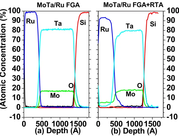
Fig. 4.3 AES depth profiling of (a) MoTa/Ru at 400°C FGA, (b) MoTa/Ru at 900°C RTA, (c) MoTa/W at 400°C FGA and (d) MoTa/W at 900°C RTA……….95
Fig. 4.4 RBS depth profiling of (a) MoTa/W at 400°C FGA, (b) MoTa/W at 900°C RTA, Two additional layers formed at MoTa and SiO2 interface at 900°C RTA……….96
Fig. 4.5 shows the Oxygen 1S XPS spectrum on the W and Ru capping at different anneals (a) W at as deposit, (b) Ru at as deposit, (c) Ru at FGA, (d) Ru at FGA and 900°C RTA...100
Fig. 4.6 W 4f XPS spectrum at as deposit condition with different sputtering times………101
Fig. 4.7 XPS spectrum of Ru 3d at surface and after sputtering for as deposit sample…….101
Fig. 4.8 XPS spectrum of Ru 3d at surface and after different time sputterings for FGA sample………102
List of Tables
Chapter 1 Introduction
1.1 Introduction to Scaling issues of MOSFET and Alternative high-k dielectrics and gate electrode
The InternationalTechnology Roadmap for Semiconductors predicts that a 35 nm
devicegeneration will require the equivalent of a sub-1.0 nm silicondioxide1. Reducing
the silicon dioxide thickness to the sub-1.0 nm regime may not be feasible because
significant leakage and reliabilityissues become major concerns below ~2.0–1.5 nm due
to direct tunneling2, which is exponentially dependent on the dielectric thickness.
Advanced high-k gate dielectrics and metal gate electrodes will be required to obtain an
equivalent oxide thickness (teq) less than 1.0 nm. Metallic gates can not only eliminate
gate depletion and boron penetration problems, but also have very low gate electrode
sheet resistance. Moreover, polysilicon gates have recently been shown to suffer from
Fermi level pinning at the interface of gate and high-k dielectrics3. This warrants the
investigation of metal gates as electrodes candidates on high-k dielectrics to determine
whether or not metal gates also suffer from Fermi Level pinning. The search for metallic
gates faces many challenges since they must have i) appropriate work functions, ii)
process compatibility with dielectric deposition, and iii) thermal and chemical interface
stability with dielectrics. To replace n+ and p+ poly-Si and maintain scaled performance,
it is necessary to identify pairs of metals with work functions that are respectively within
0.2 eV of the conduction and valence band edges of Si. This means the work function for
Table 1.1. Equivalent physical gate oxide thickness in 2005 ITRS road map.
Year 2001 2002 2003 2004 2005 2006 2007 Technology node (nm) 130 115 110 90 80 70 65 Tox (nm) 1.3-1.6 1.2-1.5 1.1-1.6 0.9-1.4 0.8-1.3 0.7-1.2 0.6-1.1
1.1.1 Alternative high k dielectrics:
As the thickness of SiO2 approaches below 1.0 nm, the leakage current increases
significantly due to direct tunneling. The high leakage current degrades the circuit
performance such as standby power, reliability, operation speed, and noise margin of
CMOS inverters. To reduce the leakage current while keeping the same equivalent oxide
thickness, a thicker film with a high dielectric constant (k) is required. Currently, the
most promising high-k materials are Hf and Zr based dielectrics. Materials properties
must meet a set of criteria to perform as successful alternative high-k gate dielectric:5
A. Permittivity and Barrier height:
Although many researchers originally assumed that selecting a dielectric with
k>25 would be necessary to replace SiO2, the more relevant consideration is whether the
desired device performance can be obtained at the prescribed operating voltage without
producing unacceptable leakage currents and reliability characteristics. It is therefore
more appropriate to find a dielectric which provides even a moderate increase in k, but
which also produces a large tunneling barrier and high-quality interface to Si. Consider
this reality situation, even a material with k~12–20 will allow a physical dielectric
thickness of 35–50 Å to obtain the teq values required for 0.1 um CMOS.5
Table 1.3 Band offset calculations for a number of potential high-k gate dielectrics.5
B. Thermodynamic Stability on Si:
For all thin gate dielectrics, the interface with Si plays a key role in determining
the overall electrical properties. Most of the high-k metal oxide systems investigated thus
an interfacial reaction barrier. Any ultrathin interfacial reaction barrier with teq<20Å will
have the same quality, uniformity and reliability concerns as SiO2 does in this thickness
regime. It is important to understand the thermodynamics of these systems, and thereby
attempt to control the interface with Si.5 Especially, we should understand the Hf–Si–O
system. Although the thermodynamic information is incomplete for the Hf–Si–O system,
the available data suggests that HfO2 and HfSiO4, as well as a large range of
(HfO2)x(SiO2)1-x compositions, will be stable in direct contact with Si up to high
temperatures6-8. This suggests that there is potential to control the dielectric-Si interface.
C. Interface quality:
An ultimate goal of any potential high-k gate dielectric is to attain a sufficiently
high-quality interface with the Si channel, as close as possible to that of SiO2. It is
difficult to obtain any material creating a better interface than that of SiO2, since typical
production SiO2 gate dielectrics have a midgap interface state density Dit~2x10¹⁰
states/cm2. Most of the high-k materials show Dit~1011–1012 states/cm2 and exhibit a large
flatband voltage (Vfb) shift >300mV (possibly from fixed charge density>1012/cm2 at the
interface)9-12. It is crucial to understand the origin of the interface properties of any
high-k gate dielectric, so that an optimal high-high-k–Si interface may be obtained.
D. Film morphology:
Most of the advanced gate dielectrics studied to date are either polycrystalline or
single crystal films, but it is desirable to select a material which remains in a amorphous
phase13. HfO
2 and ZrO2 are no exception. It is important to note there will certainly be
crystallization suppression for a given oxide will depend on composition and thermal
processing. Amorphous films that exhibit isotropic electrical properties will not suffer
from grain boundaries and can be easily deposited. Bulk thermodynamics suggests that a
phase field exists for relatively low levels of Zr or Hf in which a (ZrO2)x(SiO2)1-x or
(HfO2)x(SiO2)1-xcomposition can be obtained which will remain amorphous and stable on
Si up to high temperatures without phase separating into crystalline MSiO4 or MO2 and
SiO2.5
E. Gate compatibility:
It is also desirable to focus efforts on dielectric materials systems which are
compatible with potential metal gate materials. A key issue for gate electrode materials
research will be the control of the gate electrode work function (Fermi level) after CMOS
processing.5
F. Process Compatibility:
The deposition process for the dielectric must be compatible with current or
expected CMOS processing, cost, and throughput. Since all of the feasible deposition
techniques available occur under nonequilibrium conditions, it is certainly possible to
obtain properties different from those expected under equilibrium conditions. Therefore,
it is important to consider the various methods for depositing the gate dielectrics:
physical vapor deposition (PVD), chemical vapor deposition (CVD), atomic layer
deposition (ALD) and molecular beam epitaxy (MBE).
G. Reliability:
The electrical reliability of a new gate dielectric must also be considered critical
dielectric satisfies the strict reliability criteria requires a well characterized materials
system, a prospect not yet available for the alternate dielectric materials considered here.
This emphasizes the importance and urgency to investigate the reliability characteristics
of alternative dielectrics, as these materials are sure to exhibit subtleties in reliability that
differ from those of SiO2.5
1.1.2 Alternative metal gate electrode:
Metal gates are very desirable for eliminating dopant depletion effects and sheet
resistance constraints. In addition, the use of metal gates in a replacement gate process
can lower the required thermal budget by eliminating the need for a dopant activation
anneal in the poly-Si electrode14,15. The search for metallic gates faces many challenges
since they must have compatible work functions, thermal/chemical interface stability
with underlying dielectric and process compatibility with underlying dielectric.
Transition metals have been widely used in microelectronic industry and are a
good source from which one can select appropriate metal gates. The following table lists
Table 1.4 Work function values of transition metal elements.16
Although we can have low and high workfunction element gates, as shown in the
Table above, the low work function metal generally is a reactive element and not stable
on the dielectric17. High work function metals have process difficulty and adhesion
problems on the dielectric. So other compound metals have been investigated, such as
conducting metal oxides (In2O3, SnO2, OsO2, RuO2, IrO2, ZnO, MoO2, ReO2) and
conducting metal nitrides (WNx, TiNx, MoNx, TaNx, TaSixNy). Metal silicides such as
NiSi, PtSi, and RuTa metal alloy also have been reported recently. These will be
discussed in detail.
The compatibility of a metal gate to a dielectric is also a key issue for CMOS
associated with these two approaches are shown in Fig. 1. The first approach is to use a
metal (such as TiN) that has a work function that places its Fermi level at the midgap of
the Si substrate, as shown in Fig.1.(a). These are generally referred to as ‘‘midgap
metals.’’ The main advantage of employing a midgap metal arises from a symmetrical
threshold voltage (Vt) value for both nMOS and pMOS because by definition, the same
energy difference exists between the metal Fermi level and the conduction and valence
bands of Si. This affords a simpler CMOS processing scheme since only one mask and
one metal would be required for the gate electrode (no ion implantation step would be
required). For the case of sub-0.13 µm bulk CMOS devices, however, a major drawback
is that the band gap of Si is fixed at 1.1 eV, thus the threshold voltage for any midgap
metal on Si will be ~0.5 V for both nMOS and pMOS. Since voltage supplies are
expected to be <1.0 V for sub-0.13 µm CMOS technology, Vt~0.5V is much too large, as
it would be difficult to turn on the device. Typical threshold voltages for these devices are
expected to be 0.2–0.3 V. Compensation implants can be made in the channel to lower
the Vt but other concerns then arise regarding increased impurity ion scattering which
would degrade the channel carrier mobility. Short channel effects are also expected to
worsen with these dopant profiles in the channel. Furthermore, midgap work function
metal gate systems have been predicted not to provide a performance improvement
worthy of the added process complexity to replace Si-based gates.18
The second main approach toward metal electrodes involves two separate metals,
one for pMOS and one for nMOS devices. As shown in Fig.1 (b), two metals could be
work function value of Al could achieve Vt~0.2V for nMOS, while the higher work
functionvalue of Pt could achieve Vt~-0.2V for pMOS. In practice, elemental metal gates
have stability and adhesion problem as discussed above.
Fig.1.1 Energy diagrams of threshold voltages for nMOS and pMOS devices using (a)
1.2 Metal Gate Effective Work Function Extraction and Fermi Level Pinning Issues. 1.2.1 Effective work function definition.
The work function (φm) of a metal is the amount of energy required to raise an
electron from the Fermi level to a state of rest outside the surface of the metal (vacuum
level). Calculated using quantum mechanics, work function is found to consist of two
parts: a volume contribution, which represents the energy of an electron due to periodic
potential of the crystal and the interaction of the electron with other electrons and a
surface contribution, which is related to the possible existence of a dipole layer at the
surface. In general, the electron charge distribution around the atoms at the metal surface
is not symmetrically disposed in relation to the nucleus, so that the centers of positive and
negative charge do not coincide, resulting in a dipole layer. Moreover, the relaxation or
reconstruction associated with a surface can also lead to dipole layers. If the resulting
dipole layer has an electric dipole moment (ρ) per unit area, there will be an electrostatic
potential difference of magnitude (ρ/ε) between the vacuum and the interior of the metal.
The change in energy (qρ/ε) of an electron due to this change in electrostatic potential
constitutes part of the work function. Clearly, any modification in the surface electron
charge distribution will lead to a change in the dipole layer and h ence in work function.
Different crystallographic faces of the same crystal may also have different values of
workfunction due to surface dipoles of unequal magnitudes. For example, the work
function of Mo has different values on different face orientations.19
In measuring the metal gate work function of a MOS device, it is not possible to
dielectric, the interface dipole is modified by the metal and dielectric surface dipoles. The
relationship of interface dipoles and surface dipoles is still not known.
1.2.2 Metal Gate Fermi level Pinning.
When a metal and a dielectric form an interface, charge transfer generally occurs
across the interface. The Schottky model, where band alignment is determined solely
from the work function of the metal in vacuum and the dielectric electron affinity on an
absolute energy scale, is not usually obeyed by experimental data due to the presence of
intrinsic interface states. At clean metal surfaces, the wavefunctions of the electrons are
exponentially decaying into the vacuum. When the vacuum is replaced by the dielectric,
the propagation of the wavefunctions across the solid-solid interface is somewhat more
complicated. The tails of the conduction electron wavefunctions in the metal which
tunnel into the bandgap of the dielectric induce the gap states at interface. Those states
are called as Metal Induced Gap States (MIGS) and are an intrinsic property of
semiconductor. These states are predominantly donor-like close to the valence band (Ev),
and mostly acceptor-like near the conduction band (Ec). The energy level in the band gap
at which the dominant character of the interface states changes from donor-like to
accepter-like is called the charge neutrality level Ecnl. Charging of these interface states
creates a dipole that tends to drive the band lineup toward a position that would give zero
Fig 1.2 Energy band diagram and charging character of interface states for the
metal-dielectric interface.20
Fig. 2 illustrates the case where the metal Fermi level EF,M is above the charge
neutrality level in the dielectric ECNL,d creating a dipole that is charged negatively on the
dielectric side. This interface dipole drives the band alignment so that EF,M goes toward
ECNL,d and the effective metal workfunction φm,eff therefore differs from the vacuum metal
workfunction φm,vac. This is explained by the equation
φm,eff=φCNL,d+S(φm,vac-φCNL,d)
where S is a slope parameter that accounts for dielectric screening and depends on the
electronic component of the dielectric constant23. With larger dielectric screening, S
becomes smaller, and a higher degree of pinning to ECNL,d is experienced. From the
knowledge of both φCNL,d and S, metal workfunctions can be predicted for a variety of
materials interfaces. MIGS framework provides a convenient means for estimation of
function. On the other hand, MIGS are more numerous and decay less rapidly in HfO2, so
that Fermi level does not swing as much as that of SiO2.
Recently, Hobbs et al. report that Fermi level pinning at the polysilicon/metal
oxide interface causes high threshold voltages in MOSFET devices.3,24 Results indicate
that pinning occurs due to the interfacial Si-metal bonding. From the Vfb shift values,
they have found that pinning occurs just below the ploy-Si conduction band (CB). See
Fig. 3.
Fig. 1.3 Change of flat band potential vs. HfO2 film thickness. Showing tendency for
potentials to converge on 0.35 eV below CB edge.24
They carefully analyzed the accumulation capacitor equivalent oxide thickness
(CETacc) and inversion capacitor equivalent oxide thickness (CETinv) of an n+ and p+
MOSFET as showed in Fig.4. For the nMOS device, both CETs decrease when the SiO2
is capped with 10 cycles of HfO2. A decrease in both CETs is not what one would expect
for a dielectric stack that is capped and therefore, slightly thicker. For the pMOS devices,
the CET behavior is much different. The HfO2 cap causes the CETinv to increase whereas
with an increase in the poly-Si depletion for the p+ gate. To explain this behavior, they
proposed that Hf atoms terminate the HfO2 at the poly-Si-HfO2 interface. For the n+ gate,
the decrease in both CETs is consistent with the idea that Hf atoms at the interface are
essentially becoming part of poly-Si which makes the gate display a metal-like behavior.
The work function of Hf is about 3.9 eV. It is close to the n+ Fermi level and also not too
far away from the Fermi pinning location as indicated by the above data. So they
speculated that the quasi-Fermi level of the interfacial Hf atoms is close to that of n+ poly
Si. The Hf/poly-Si Fermi level alignment in conjunction with the metallic properties of
the thin Hf layer explains the decrease in both CETs for the n+ gate. For the case of a p+
doping, the poly-Si Fermi level is located near the Si valence band edge which is more
energetically distant from the Hf work function than for an n+ poly Si gate. Since there
are not enough interfacial Hf atoms to form a true Hf metal, the authors speculated that
the poly-Si depletion for a p+ gate becomes worse due to a shift of the poly-Si Fermi
level toward the Hf quasi-Fermi level.
Based on the experimental data, Robertson et al. proposed a more accurate and
detailed model.25 This report considered the cause of Fermi pinning to be extrinsic effects
due to specific bonding configurations. They argue that the observed effect is not due to
MIGS because the pinning by MIGS should center on the charge neutrality level of Si,
which is 0.3 eV above the valance band (VB) edge whereas, experimentally the pinning
seems to be centered about 0.35 eV below the conduction band (CB) edge. Also, a MIGS
model would not explain the effect in thin overlayers of HfO2 on SiO2 because MIGS of
HfO2 takes a few layers to develop. They proposed that Hf-Si interface bonds can be
created on a fully oxygen (O) terminated interface by either substituting Si at O
interfacial sites or by forming interfacial O vacancies. Their calculation results suggest
that there are a range of different interface configurations with mixed Hf-O and Hf-Si
bonding. Hf-Si bonding tends to introduce states across the Si band gap rather than
specific deep gap states. The Fermi level tends to lie at a similar energy in each case,
about 0.3 eV below the CB. Therefore, the presence of Hf-Si interface bonds is likely to
pin the Fermi level in the upper half of the Si band gap.
Yang et al. also observed similar Vfb shifts of poly-Si on HfO2 and proposed a
model considering acceptor- or donor-like interface states at the poly-Si and HfO2
interface.26 Their conclusion is that the flatband voltage shift for HfO2 films in
nMOSFETs and pMOSFETs is caused by the Fermi level in the gate material and is
independent of the substrate type. For n-type poly-Si, acceptor-like interface states are
electrically active and lead to positive flatband voltage shift. Donor-like interface states
are electrically active in p-type poly-Si gates resulting in negative flatband voltage shift.
than for nMOSFETs and is probably due to the high poly-Si depletion for the p-type
poly-Si.
Fig. 1.5 Schematic band diagrams of acceptor- and donor-like interface states at
interface.26
1.2.3 Effective work function extraction on SiO2 and High-k dielectrics.
Electrical properties such as work function, dielectric constant, leakage current
density, interfacial trap density, oxide trapped charge, dielectric integrity, mobility and
reliability are all critical concerns for the development of advanced gate stacks.
extracted from C–V analysis by taking the y intercept of Vfb vs. teq curves. The work
functions of the metal gate can also be extracted from the barrier heights of gate\SiO2 by
using Fowler–Nordheim (FN) tunneling analysis. The Fowler–Nordheim current is given
by JFN=AEox2exp[-B/Eox]28-30. The parameter A and B depend on the barrier height and
the effective mass of the tunneling electron in the oxide. Eox is the electric field across the
dielectric.
Fig. 1.6 Energy diagram of Metal gate/SiO2/p-Si structures for FN tunneling.
On the high-k dielectrics, the work function extraction becomes much more
complicated. For the C-V method, Vfb = φm–Φs–Qfteq/εox will not be accurate due to
additional interfacial layer formed at high-k dielectric and Si substrate. Jha et al.
developed a charge model by evaluating the metal gate workfunction on high-k/SiO2
stacks instead of the high-k dielectric only31. The fixed charge at the high-k/SiO2
interface and SiO2/Si interface can be extracted by using varying thickness of high-k or
SiO2 stacks under the assumption that the bulk charge can be ignored. Then, a more
neglect the bulk charge. So Vfb = φm–Φs–Qfteq/εox+Vdip. Qf is the fix charge at the
high-k/Si interface and Vdip is the additional term from gate/high-k dipole layer.
The Fowler–Nordheim (FN) tunneling analysis on high-k also faces several
challenges. The Fowler–Nordheim current is given by JFN=AEox2exp[-B/Eox]. The
parameter A and Bdepend on the barrier height and the effective mass of the tunneling
electron in the oxide. Currently, there is not enough data on the effective mass of
electrons through the high-k dielectrics currently under investigation. In addition, even
for the same high-k dielectric, the effective mass may be different for different deposition
processes/compositions. Moreover, the high-k dielectric itself is not very uniform across
the depth since an interfacial layer can form. So the FN model can not be easily applied
1.3 Recent research on metal gate electrodes 1.3.1 Fully-Silicided (FUSI) Gates:
Many groups have recently intensively investigated Fully-Silicided (FUSI) gate
electrodes. Gusev et al. reports that that FUSI/HfSixOy gate stacks offer both significant
gate leakage reduction and drive current improvement at equivalent inversion thickness
(Tinv)~ 2 nm due to: (i) elimination of poly depletion effect, ~ 0.5 nm and (ii) high
mobility of HfSixOy.32 They also demonstrate that threshold voltage for both PFETs and
NFETs can be adjusted from midgap to the values of Vt(PFET)~ -0.4 V and Vt(NFET) ~
+ 0.3 V by poly-Si predoping by implantation (Al or As) and FUSI alloying.
Significantly improved charge trapping (Vt stability) was found in the case of NiSi/
HfSixOy compared to the same gate electrode with HfO2 dielectric.
Takahashi et al. presents a new threshold-voltage control technique for FUSI
metal/high-k gate stacks which are suitable for 45nm node CMOS.33 The key is the phase
control of FUSI Ni-silicide by changing the Ni film thickness prior to silicidation anneal.
As a result, Ni3Si and NiSi2 are formed whose effective workfunctions on HfSiON are
found to be 4.8eV and 4.4eV, respectively. This is largely displaced from the Si midgap
by ±0.2 eV. Meanwhile, the dopant segregation method, known to be successful in Vt
control of NiSi on SiO2, did not work on HfSiON. With Ni3Si-PMOS and NiSi2-NMOS
transistors, a wide range of Vt tuning is achieved. At the same time, leakage suppression
merit is better than the 45nm node targets at Tinv around 2.0 nm. Also, the phase
controlled fully silicided (PC-FUSI) devices show excellent mobility characteristics.
1.3.2 Metal Nitride Gates:
Incorporating nitrogen (N) into the metal to modulate workfunction and improve
stability is also being widely investigated. The characteristics of MOSFET using TaN
gate electrode and HfO2 dielectric were investigated by Lee et al.35. Using TaN
electrodes, the gate dielectric thickness of MOSFETs with HfO2 was scaled down to 11 Å
with very low leakage current even after the high temperature conventional CMOS
process. The resistivity of stoichiometric TaN was low (~200 µΩ-cm) and the work
function was 4.15 eV.
Our group has recently reported that TaSixNy films on SiO2 provide work function
(4.2 ~ 4.3eV) compatible with NMOS devices and good thermal stability up to 1000ºC
resulting in minimal change of teq while demonstrating low leakage current36. The
improved stability of TaSixNy gates is attributed to the presence of Si and N in the gate
electrode which can improve the film microstructure and the diffusion barrier properties
of the gate-dielectric interface.
Park et al. studied ternary metal nitride gates such as Ti1-xAlxNy (TiAlN) on
high-k gate dielectrics (ZrO2, HfO2) annealed up to 950°C.37,38 They found that stoichiometric
TiAlN (y~1) exhibited highly robust p-type gate electrode (p-TiAlN) properties
demonstrating a work function of ~5.1 eV and an excellent gate oxide integrity against
the thermal budget of conventional Si CMOS process. The N-deficient TiAlN (y < 1) had
work function compatible with n-type electrodes (n-TiAlN) but showed limited thermal
stability. Other groups have also reported MoN, WN and TiN as the alternative metal
1.3.3 Metal Alloys and Metal Stacks:
Polishchuk et al. proposed a dual metal gate CMOS integration scheme which
consisted of depositing a stack consisting of two metals followed by a metal
interdiffusion to achieve low threshold voltages for both nMOSFET and pMOSFET46. It
was demonstrated that intermixing of Ti-Ni metal stacks produces gate electrodes with
3.9 eV and 5.3 eV work functions for n-MOS and p-MOS devices respectively.
Our group has reported binary metal alloys of Ru and Ta as candidates for CMOS
gate electrodes.47 It was demonstrated that Ru-Ta alloys are excellent NMOS gate
electrode candidates since they exhibit low work functions and demonstrate superior
thermal stability compared to Ta. Moreover, by increasing the Ru concentration of this
alloy, excellent PMOS gate characteristics were achieved. Lee et al. has also reported that
a Ta/Ru metal stack can achieve excellent metal gate electrode characteristics for CMOS
application by metal interdiffusion.48,49
Jeon et al. demonstrated that the work function of a metal gate can be varied by
inserting a very thin metal layer (“Metal A”) between a thick metal (“Metal B”) and the
gate dielectric.50 The flat band voltage of the MOS capacitor structure can be controlled
within the range bounded by Metal A and Metal B, individually, as demonstrated with
various stacked bi-metal layers. For continuous thin layers, they speculate that the work
function tunability may be due to the drastic change of the electron density in the thin
continuous metal layer in direct contact with a bulk metal. Nonuniform thin layers also
appear effective for workfunction tuning as well and the observed Vfb shift is attributed to
On theoretical work on metal gate electrodes, Park et al. recently studied the work
function of metal multilayers and monolayers on a bulk metal using the first principle
pseudopotential method within the local density approximation in order to find a way to
modulate the work function of metal gate electrodes51. Various multilayer stacks and
bilayer stacks of two systems, Al–Pt and Al–Ni, were examined. It was found that two or
three layers of the metal are enough to shift the work function to that of the surface metal.
Also, it was found that even a submonolayer could affect the work function of the bulk
metal significantly.
Fig. 1.7 Work functions of dual metal contact: (a) Al on Pt and Pt on Al (b) al on Ni and
1.4 Goal of Research on Metal Gate electrodes.
My research goal was to examine metal alloys for CMOS application. A metal
alloy is a material that exhibits properties of a metallic material and is made from
multiple elements. There are two types of binary metal alloys: metallic compound and
solid solution. For a metallic compound, the two elemental metals have limited solubility
in each other and new compound phase can be formed in addition to the elemental metal
phases. In the solid solution, the two metals have unlimited solubility in each other and
have only one solution phase.
We investigated a key set of metal gate alloys, such as RuY and MoTa, in
capacitor structures and evaluated their electrical and structural properties. RuY can
form a metallic compound and MoTa is a solid solution system. Rutherford
backscattering spectroscopy and Auger electron spectroscopy was performed to
investigate the composition of the films. The microstructures of the films was
characterized by X-ray diffraction (XRD), X-ray photoelectron spectroscopy (XPS), and
transmission electron microscopy (TEM) to evaluate the thermal stability of the films.
We evaluated different metal gates on different high-k dielectrics. Fermi level
pinning was studied. High-k dielectrics were analyzed by XPS to study the composition
differences. The role of oxygen and carbon on the surface and within the dielectric also
was investigated. This may cause very different electrical properties of metal gates on the
high-k dielectrics.
We also studied tuning effective work function by the interfacial dipole. The
interfacial dipole was generated from the interfacial charge trapping layer by the thin
studied to promote the thermal stability and tune the work function value to higher by
AlTaN alloy for pMOS gate application. Advanced capping layers were investigated for
1.5 References
1. International Technology Roadmap for Semiconductors, 2005 edition (S. I.
Association, Austin, TX, 2005).
2. D. A. Buchanan and S.-H. Lo, Microelectron. Eng. 36, 13 (1997).
3. C. Hobbs, et al. Symposium on VLSI Technology Digest of Technical Papers. (2003).
4. Indranil De, Deepak Johri, Anadi Srivastava, C. M. Osburn, Solid-State Eelctronics,
44, 1077 ( 2000).
5. G. D Wilk et al, “H-k gate dielectrics: Current status and materials properties
considerations,” JAP. Vol.89, Number 10, 15 May, 2001.
6. I. Barin and O. Knacke, Thermochemical Properties of Inorganic Substances
(Springer, Berlin, 1973).
7 L. B. Pankratz, Thermodynamic Properties of Elements and Oxides (U.S. Dept. of
Interior, Bureau of Mines Bulletin 672, U.S. Govt. Printing Office, Washington, D.C.,
1982).
8 S. P. Murarka, Silicides for VLSI Applications (Academic, New York,1983).
9 L. Kang, B. H. Lee, W. J. Qi, Y. J. Jeon, R. Nieh, S. Gopalan, K. Onishi, and J. Lee,
“Electrical characteristics of highly Reliable ultrathin hafnium Oxide Gate Dielectric,”
IEEE Electron Device Letters, vol. 21, p. 4, 2000.
10 B. H. Lee, L. Kang, W. J. Qi, R. Nieh, Y. Jeon, K. Onishi, and J. C. Lee, “ Untrathin
hafnium Oxide with low leakage and excellent reliability for alternative gate dielectric
11 B. H. Lee, L. Kang, W. J. Qi, R. Nieh, Y. Jeon, and J. C. Lee, “Thermal stability and
electrical characteristics of ultrathin Hafnium oxide gate dielectric reoxidized with rapid
thermal annealing,” Appl. Phy. Lett., vol. 76, p. 1926, 2000.
12 B. H. Lee, Y. Jeon, K. Zawadzki, W.-J. Qi, and J. Lee, “Effects of interfacial layer
growth on the electrical characteristics of thin titanium oxide films on silicon,” Appl.
Phys. Lett., vol. 74, no. 21, p. 3143, 1999.
13. W. Lee et al., “Gate quality doped high k films for CMOS beyond 100nm:3-10nm
Al2O3 with low leakage and low interface states,” Int. Electron Device Tech. Dig., p. 605,
1998
14. A. Chatterjee, R. A. Chapman, K. Joyner, M. Otobe, S. Hattangady, M. Bevan, G. A.
Brown, H. Yang, Q. He, D. Rogers et al., Tech. Dig. Int. Electron Devices Meet. 1998, p. 777.
15. Y. Ma, Y. Ono, L. Stecker, D. R. Evans, and S. T. Hsu, Tech. Dig. Int. Electron
Devices Meet. 1999, p. 149.
16. E.D. Eastman et al, “Photoelectric work functions of Transition, Rare-Earth and
Noble metals”, Phys. Rev. B ,Numb.1 Vol.2, 1 July 1970.
17 V. Misra, G. P. Heuss, and H. Zhong, “Use of metal-oxide-semiconductor capacitors
to detect interactions of Hf and Zr gate electrodes with SiO2 and ZrO2” Appl, Phy. Lett.,
vol. 78, p. 4166, 2001.
19 Q. Lu, R. Lin, P. Ranade, T.-J. King, and C. Hu, “:Metal gate work function
adjustment for future CMOS technology” IEEE Symp. on VLSI Technology Tech. Dig.,
p. 49. 2001.
20. Yee-Chia Yeo et al, “Effects of High-k Gate Dielectric Materials on Metal and
Silicon Gate Workfunction”.
21. J. Tersoff, “Theory of semiconductor heterojunctions: The role of quantum dipoles,”
Phys. Rev. B, vol. 30, pp. 4874–4877, Oct. 1984.
22. F. Capasso and G. Margaritondo, Eds., “The theory of heterojunction band lineups,”
in Heterojunction Band Discontinuities. Amsterdam, The Netherlands: Elsevier, 1987,
ch. 1.
23. W. Mönch, “Electronic properties of ideal and interface-modified metal–
semiconductor interfaces,” J. Vac. Sci. Technol. B, vol. 14, pp. 2985–2993, Jul./Aug.
1996.
24. C. Hobbs et al, “Fermi-Level Pinning at the Polysilicon/Metal Oxide Interface”.
IEEE, Transaction on Electron Devices, Vol.51, No.6, June, 2004.
25. K. Xiong, P.W. Peacock and J. Robertson, “Fermi level pinning and Hf-Si bonds at
HfO2: Polycrystalline silicon gate electrode interfaces.” APL, 86, 2005.
26. C. W. Yang, APL, Vol. 83, NO. 2. 14 July 2003.
27. You-Seok Suh, Greg P. Heuss, and Veena Misra, Appl. Phys. Lett. 80, 1403 (2002).
28. J. M. Lenzlinger and E. H. Snow, J. Appl. Phys. 40, 278 (1969).
29. M. Depas, B. Vermeire, P. W. Mertens, R. L. Van Meirhaeghe, and M. M.Heyns,
Solid-State Electron. 38, 1465 (1995).
31. Rashmi et al, “A capacitance-based methodology for work function extraction for
metals on H-k”. EDL, Vol.25, No.6, June 2004.
32. E. P. Gusev et al, “Advanced gate stacks with fully silicided fates and high-k
dielectrics: Enhanced performance at reduced gate leakage”. IEDM, 2004.
33. K. Takahashi et al, “Dual workfunction Ni-silicide/HfSiON gate stacks by
phase-controlled full-silicidation (PC-FUSI) technique for 45 nm-node LSTP and LOP devices.
IEDM, 2004.
34. T. Nabatame et al, “Partial silicides technology for tunable work function electrodes
on high-k gate dielectrics-Fermi level pinning controlled PtSix for HfOx(N) pMOSFET”,
IEDM, 2004.
35. B. H. Lee, L. Kang, W. J. Qi, R. Nieh, Y. Jeon, and J. C. Lee, “Characteristics of TaN
gate MOSFET with ultrathin hafnium oxide (8-12Å),” IEEE Int. Electron Devices Meet.
Tech. Dig. p. 39, 2000.
36 Y. S. Suh, G. P. Heuss, H. Zhong, and V. Misra, “Electrical Characteristics of TaSixNy
Gate Electrodes for Dual Gate Si-CMOS Devices,” IEEE Symp. on VLSI Technology
Tech. Dig. p. 47, 2001.
37 D. G. Park, T. H. Cha, K. Y. Lim, H. J. Cho, T.-K. Kim, S. A. Jang, Y. S. Suh, V.
Misra, I. S. Yeo, J. S. Roh, J. W. Park, and H. K. Yoon, “Robust Ternary Metal Gate
Electrodes for Dual Gate CMOS Devices,” IEEE Int. Electron Devices Meet. Tech. Dig.,
p. 671, 2001.
38. Tae-Ho Cha et al. “ Work function and thermal stability of Ti1-xAlxNy for dual
39. Q. Lu et al., “Dual –metal gate technology for deep-submicron CMOS transistors,”,
VLSI, pp72-73, 2000.
40 Q. Lu, R. Lin, P. Ranade, T.-J. King, and C. Hu, “:Metal gate work function
adjustment for future CMOS technology” IEEE Symp. on VLSI Technology Tech. Dig.,
p. 49. 2001.
41 J. C Hu et al., “Feasibility of using W/TiN as metal gate for conventional 0.13µm
CMOS technology and beyond,” IEEE Int. Electron Devices Meet. Tech. Dig. p. 825,
1997.
42 A Chatterjee et al., “ Sub-100nm gate length metal gate NMOS transistors fabricated
by a replacement gate process,” IEEE Int. Electron Devices Meet. Tech. Dig. p. 821,
1997.
43 K. Nakajima et al., “Work function controlled metal gate electrode on ultrathin gate
insulators,” Symp. on VLSI Tech. Dig., p. 95, 1999.
44 T. Yamada, et al., “The metal gate MOS reliability with the improved sputtering
process for gate electrode”, IEEE Int. Electron Devices Meet. Tech. Dig., 1999.
45. Dae-Gyu Park et al., “Novel Damage-free direct metal gate process using atomic
layer deposition”. VLSI, 2001.
46. I. Polishchuk, P. Ranade, T.-J. King, and C. Hu, “Dual work function metal CMOS
technology using metal interdiffusion,” IEEE Electron Device Lett., vol. 22, p. 444, 2001.
47. H. Zhong, S. N. Hong, Y.-S. Suh, H. Lazar, G. Heuss, and V. Misra, “Properties of
Ru-Ta Alloys as Gate Electrodes For NMOS and PMOS Silicon Devices” in IEEE Int.
48. Jaehoon Lee et al., “Tunable work function dual metal gate technology for bulk and
non-bulk CMOS”. IEDM, 2002.
49. Jaehoon Lee et al., “Compatibility of dual metal gate electrodes with high-k
dielectrics for CMOS”. IEDM, 2003.
50. I.S. Jeon et al. “A novel methodology on tuning work function of metal gate using
stacking bi-metal layers”. IEDM, 2004.
51. Seongjun Park et al., “Ab initio study of metal gate electrode work function”, APL,
Chapter 2 Physical and Electrical Analysis of RuxYy Alloys for CMOS Gate
Electrodes 2.1 Introduction
This chapter describes RuxYy as a novel candidate for dual metal CMOS
applications. The characterization of RuY alloys indicate that the effective work function
can be controlled from 3.9eV to 5.0eV as the Yttrium composition in the RuxYy is
decreased film for both PMOS and NMOS application. From XPS analysis, it was found
the Ru 3d peaks do not change as the Y composition is changed, indicating the Ru-Y
bonding is very weak or undetectable in RuxYy film. However, it was also found that Y
reacts with the underlying SiO2 to form yttrium silicate. In addition, in-situ XRD results
did not detect the presence of Ru-Y compound in the RuxYy films. C-V characterization
indicated that the oxide thickness decreased as the Y composition increased. We
extracted the effective barrier height of RuxYy at the metal-oxide interface via
Fowler-Nordheim current analysis. The barrier height decreases as the Y composition increased.
This agrees with the change of RuxYy work function which was extracted from the C-V
analysis.
2.1.1 Introduction of prior work on RuTa alloy
The InternationalTechnology Roadmap for Semiconductors predicts that a 35 nm
devicegeneration will require the equivalent of a sub-1.0 nm silicondioxide1. Reducing
the silicon dioxide thickness to the sub-1.0 nm regime may not be feasible because
significant leakage and reliabilityissues become major concerns below ~2.0–1.5 nm due
to direct tunneling2, which is exponentially dependent on the dielectric thickness.
oxide equivalent thickness less than 1.0 nm. Metallic gates can not only eliminate gate
depletion and boron penetration problems, but also have very low gate sheet resistance.
Moreover, polysilicon gates have recently been shown to suffer from Fermi level pinning
at the interface of gate and high-k dielectrics3. This warrants the investigation of metal
gates as electrodes candidates on high-K dielectrics. The search for metallic gates faces
many challenges since they must have i) appropriate work functions, ii) process
compatibility with dielectric deposition, and iii) thermal/chemical interface stability with
dielectrics. To replace n+ and p+ poly-Si and maintain scaled performance, it is necessary
to identify pairs of metals with work functions that are respectively within 0.2 eV of the
conduction and valence band edges of Si, i.e., the work function for NMOS and PMOS
gates must be near 4eV and 5eV, respectively4.
Alternative metal gates include elemental metals, metal nitrides, metal silicides or
other metallic alloys5,6,7. It has been reported that the work function of metal alloys can
be linear or nonlinear depending on the alloy type and compostion7. We have recently
reported on the electrical and material characteristics of Ru-Ta alloy films and shown that
when the Ta percentage in the Ru-Ta alloys lies between 40% and 54%, the films exhibit
excellent properties as NMOS gates, whereas, when the Ta percentage is less than 20% ,
the alloys exhibit excellent properties as PMOS gates8. For an AxB1-x alloy, it is natural to
consider that the work function f(x) changes with x as Φαverage(x)= xφA+(1-x)φB, where φA
and φB represent the work function of pure elements. Ni-Cu alloy system was found to
have close linear relation to its component work functions9. However, this is not
the work function falls below the linear interpolation9. The relationship between charge
transfer in alloys and electronegativity work function resulting from the modified
electron-electron Coulomb has been used to explain the non-linear relationship between
the work function and alloy composition11. For binary alloy systems, a nonzero difference
in electron-per-atom ratio for the constituents will lead to a transfer of charge in the alloy,
which is related to electronegativity and work function. In the case of Ru-Ta alloys, it
was observed that the work function depended non-linearly on the composition. The
lowest work function for Ru-Ta thermally stable films was found to be near 4.3eV.
Fig. 2.1 The effective work function of RuTa alloy decreases as Ta sputtering power
percent increases.
4
4.2
4.4
4.6
4.8
5
5.2
0
20
40
60
80
100
W
o
rk
f
u
nc
ti
on
(e
V
)
Ta Percent ( %)
2.1.2 Introduction of RuY alloy
In this chapter, we report the physical and electrical characteristics of a new
RuxYy gate in which a potential advantage is the possibility of obtaining work functions
lower then 4.3eV owing to the presence of Y in the alloys. Table 2.1 shows phase
diagram of RuY alloy. RuY is intermetallic alloy with line single phase compounds.
The structure of Ru is hcp and its work function is about 5.0 eV with a resistivity
of ~ 7Ωµ.cm at 25 °C. The melting point of Ru is 2427 °C. In addition, Ru oxide is
conducting and Ru is easy to be dry etched. The structure of Y is hcp. Y work function is
about 3.1-3.3 eV and resistivity is 59.6Ωµ.cm at 25 °C. The melting point is about 1522
°C.
2.2 Electrical characterization of RuY alloy 2.2.1 C-V analysis of RuY alloys
Field oxide (3000 Å) isolated overlap capacitors were fabricated on n and p-type
wafers and liftoff was used to define the gate electrodes. Thermally grown SiO2 with
thicknesses of 30–90 Å were used as dielectrics. RuxYy gate electrodes were deposited by
co-sputtering Ru and Y targets in a RF magnetron sputtering system. The targets were 2
inches in diameter with 99.9% purity. The Ru sputtering power was fixed at 100W and
the Y sputtering power was varied from 5W to 100W. The base pressure of the sputtering
chamber was <5×10⁻⁸ Torr. All samples were subjected to a forminggas annealing at
400°C for 30 min prior to characterization. Ru-Y bonding information was obtained from
the X-ray photoelectron spectroscopy (XPS) and RuxYy composition was obtained from
Auger Electron Spectroscopy (AES). In addition, in-situ x-ray diffraction analysis was
performed. Capacitance-voltage (C-V) and current-voltage (I-V) characteristics were
obtained using HP4284 LCR meter and HP4155, respectively. The capacitance was
measured on an area equal to 2.5x10⁻⁵cm2 at 1MHz. The flat-band voltage (VFB) and
theoretical value of silicon oxide thickness (Tox) for the capacitors were obtained by
using NCSU CV program12. The work function was extracted by measuring VFB vs.
oxide thickness for various samples and the barrier heights were extracted by applying
Fowler-Nordheim analysis.
The electrical characteristics of the film were analyzed via C-V and I-V analysis.
The flatband voltage decreased progressively with the Y compositions increased as
shown in Fig. 2.2. Thework function of the RuxYy gate was determined using theflatband
fromC–V analysis by taking the y intercept of VFB vs.Tox curves. Fig. 2.3 shows the y
intercept of VFB vs. Tox curves of RuY alloys. The work function decreases as Y
composition increases. However, it was also found that the accumulation capacitance
continuously increased as the Y composition increased. This increase in Cacc is
attributed to a decrease in the SiO2 thickness and/or conversion of the SiO2 thickness into
a high-K layer. The result of this reaction could be an yttrium silicate layer13,14. Similar
VFB shifts and work function changes can be achieved from p-type substrate by various
Fig. 2.2 C-V curves of different composition RuY alloys on n-Si and p-Si at 400°C FGA.
-3
-2
-1
0
1
2
3
4.0x10
-128.0x10
-121.2x10
-111.6x10
-112.0x10
-112.4x10
-112.8x10
-113.2x10
-11Ru sputtering power 100W
Ru only
Gate Volatage(V)
Capacitance(F)
Y 100W
Y 75W
Y 50W
Y 30W
Y 20W
Y 5W
1M Hz, SiO
2n-Si
-2
-1
0
1
2
3
5.0x10
-121.0x10
-111.5x10
-112.0x10
-112.5x10
-113.0x10
-113.5x10
-111M Hz, SiO
2Gate Volatage(V)
Cap
a
citance(F)
Ru sputtering power 100W
Fig. 2.3 VFB vs. EOT of RuY alloys on p-Si and n-Si at 400°C FGA.
20 30 40 50 60 70 80 90 100
-1.5 -1.2 -0.9 -0.6 -0.3 0.0 Y 20W Y 15W Y 10W Y 5W Ru only Ru 100W FGA Y composition incr ea se Flatband Vo ltag e (V) EOT (A)
400C FGA on SiO
2/p-Si
20 30 40 50 60 70 80
-1.0 -0.5 0.0 0.5 1.0 1.5
400C FGA SiO
2/n-Si
Ru 100W
FGA
Flatba
nd Voltage (V)
2.2.2 I-V analysis and effective work function of RuY alloys
The work functions of the above films have also been compared with the barrier
heights of RuxYy thin films by using Fowler–Nordheim (FN) tunneling analysis as shown
in Fig. 2.4. The Fowler–Nordheim current is given by JFN=AEox2exp[-B/Eox]15-17. The
parameter A and Bdepend on the barrier height and the effective mass of the tunneling
electron in the oxide. As shown in Fig 2.5, the extracted effective barrier height of
various Ru-Y compositions exhibit the same trend as C-V extracted work function. The
work function changes from 5.0ev to 3.9ev as the Y sputtering power percentage is
increased from 0 to 50% in the RuxYy films. This indicates that both NMOS and PMOS
work functions were attainable with this alloy system.
Fig. 2.4 I-V curves of different composition RuY alloys on p-Si at 400°C FGA. -16 -14 -12 -10 -8 -6 -4 -2 0 1E-15
1E-11 1E-7 1E-3 10
Y 50W Y 75W Y 100W Y 30W
Ru sputtering power 100W As Y increase,
breakdown voltage decrease
I g
(A)
Vg (V)
50umx50um
Y 5W
Fig. 2.5 Effective work functions and barrier heights of RuY alloys on SiO2 at 400°C
FGA.
0 10 20 30 40 50
3.8 4.0 4.2 4.4 4.6 4.8 5.0
SiO
2Y Sputtering power percent Work function Barrier height R u -Y wo rk fu n c tio n (eV) 2.8 3.0 3.2 3.4 3.6 3.8 Ru-Y /SiO 2
Barrier height (eV
2.3 Material analysis of RuY alloys 2.3.1 AES analysis of RuY alloys
RuxYy samples of three different compositions were analyzed by XPS, XRD and
AES. The samples were prepared by co-sputtering Ru at 100Watts and Y at various
powers. The thickness of the films was ~500A. For the XPS and XRD analysis, no
capping layer was deposited, whereas for AES a 500Å Ru capping layer was used to
obtain the depth profile. All samples were subjected to a forminggas annealing at 400°C
for 30 min. Table 2.2 summarizes the sputtering conditions, the atomic composition and
the extracted C-V work function for the three samples (Y5,Y20,Y50). As shown, the Y
atomic percentage does not depend linearly on the percent sputtering power.
Table 2.2 Compositions and sputtering conditions of Ru-Y films of sample Y5,Y20,Y50.
sample
Name
Ru sputtering
power W
Y sputtering
power W
Y power
percentage
Y atomic
composition(AES)
Φm eV
Y5 100 5 4.8% 2% 4.75
Y20 100 20 16.7% 6% 4.35
2.3.2 XPS analysis of RuY alloys
From the Ru 3d XPS spectrum shown in Fig.2.6, it is found that the Ru 3d5/2
peaks of the above three samples do not shift as the Y atomic composition is increased.
The Ru 3d5/2 binding energy also stays fixed at 280.1eV in all three samples. This binding
energy is as the same as the value as pure Ru. The spin-orbit splitting between 3d5/2 to
3d3/2 of all three samples also stays ~ 4.1eV, thereby indicating that either Ru-Y binding
is not occurring or is very weak or undetectable with XPS analysis.
The Y 3d XPS spectrum is shown in Fig.2.7. As the Y composition in the films is
increased, the Y 3d peaks become higher and broad. The pure Y 3d5/2 binding energy is at
156.0eV, while the Y 3d5/2 binding energy in Ru-Y samples is observed to be close to
157.0 eV. This shift is attributed to the strong Y-O bonding13 instead of the Ru-Y
bonding since there is no evidence of bonding shift in Ru binding energy. The peak
broadening due to the presence of both Y-Y bonding (156.0eV) and Y-O bonding (Y2O3,
156.8eV). As mentioned above, the samples for XPS analysis did not have a capping
layer on top of the RuxYy films. Since Y has a very strong affinity towards oxygen, the
surface of the film could have been easily oxidized. The higher the Y composition, the
more oxidation occurrs in the film and the Y 3d peaks broaden. In addition to surface
oxidation, Y may also react with the underlying SiO2. It has been reported that the Y-O
bond is more favorable than Si-O bond, since the free energy of formation per oxygen
atom (–∆Gf) (at 25 °C) is 2.40×10⁻²² kcal for Y2O3 compared to 1.70×10⁻²² kcal for
SiO214. This suggests that Y in the gate electrode can react with the SiO2. Our C-V
From the XPS analysis shown above, the Ru-Y bonding was not detected
suggesting that it is either is very weak or no Ru-Y bonds were formed. The lack or weak
Ru-Y bonding can result in the reduction of SiO2 which decreases the dielectric
thickness. The result of this reaction could be an yttrium silicate layer13.
Fig. 2.6 Ru 3d XPS spectrum shows no RuY compound formed.
290 285 280 275
Ru 3d
5/2280.1 eV
Ru 3d
3/2284.27 eV
Y50
Y20
Y5
In
ten
sity
(A.U.)
Fig. 2.7 Y 3d and O 1s XPS spectrum show that Y is oxided at sample surface.
540
535
530
525
520
Intensity
(A
.U
.)
Binding energy (eV)
O 1s
Y5
Y20
Y50
Y
2O
3O 1s 531.0 eV
164
162
160
158
156
154
152
Intensity (A.U.)
Binding energy (eV)
Y
2O
3Y50
Y20
Y5
Y 3d
5/2156.0eV
2.3.3 XRD analysis of RuY alloys
Fig.2.8 shows the in situ XRD data of sample Y50, which was annealed from
100°C to 1100°C. It was found that the film does not crystallize into Ru-Y compound but
rather phase separates into Ru and Y. Also, there is an indication of interaction between
Y and O from the low angle peaks. This observation is in agreement with the XPS results
shown above and also confirms that Ru-Y is not dominant. No Ru-Y compound was
found in low Y composition sample Y5, Y20 as well.
Fig. 2.8 shows the in-situ XRD data of sample Y50, which was annealed from 100°C to
Fig.2.9 shows the in-situ XRD data of RuY alloy and pure Ru indicating that alloy
reduced the element metal grain size.
RuY
The above analysis can also explain why RuxYy is not stable on SiO2 while
RuxTay is stable on SiO2, because RuxTay forms strong single phase Ru-Ta bonding in the
optimized composition window but RuxYy does not. The stability difference between
RuxTay and RuxYy originates from the physical bonding difference of the two films. The
Ru-Y phase diagram suggests that the Ru-Y single phase is a line compound making it
difficult to achieve a single phase. It is not yet clear how the presence of multiple phases
affects the electrode/dielectric stability. Fig.2.9 shows the in-situ XRD data of RuY alloy
and pure Ru indicating that alloy reduced the element metal grain size. This data
demonstrates one of the advantages of alloy by reducing grain size to achieve more
uniform gate film and more uniform effective work function for the nano-size device
applications.
In summary, we have investigated the physical and electrical properties of RuxYy
thin films of various compositions. From C-V analysis we obtained the effective work
function of Ru-Y thin films to range from 5.0eV to 3.9eV which is suitable for dual metal
gate CMOS. Both XPS and XRD analysis suggests that there is no strong Ru-Y bonding
in films. The rich Y film was found to be not stable on SiO2 dielectrics because of the
high oxygen affinity of Y. However, RuxYy thin films may be stable on the future high-k
dielectrics such as Y2O3, so RuxYy thin film may still be a candidate for low temperature
process, especially due to its large range of work function. More over, RuY has smaller
grain size than Ru which demonstrates one of the advantages of alloy by reducing grain
size to achieve more uniform gate film and more uniform effective work function for the
nano-size device applications. The difference in RuxTay and RuxYy in terms of bonding