Switched Capacitor Boost Converter
Mahadevaswamy HM 1, Pradeep K Peter2, Dr M Satyendra Kumar 3
PG Student, Department of Electrical and Electronics Engineering, NMAMIT, Nitte, India1 Scientist/Engineer-SG, ISRO Satellite Centre, Bengaluru, India 2
Professor, Department of Electrical and Electronics Engineering, NMAMIT, Nitte, India 3
ABSTRACT: Switched capacitor DC-DC converter (SCC) provides DC-DC conversion with the help of capacitor where the inductor and transformer are neglected and not considered. The SCC can be used to step up, step down or invert the given supply voltage. The SCC converters are used for the low power applications in the aerospace industry. The switched capacitors converter reduces the size and weight of the converter when compared to the conventional DC-DC converters.
KEYWORDS: Switched capacitor converters (SCC), Equivalent series resistance (ESR).
I. INTRODUCTION
Switched capacitor DC–DC converter is used to convert the DC voltage from one level to another level without the use of inductors or transformers this increases the power density of the converter because the magnetic components are not used in the converter. There are different topologies of the SCC like the Dickson charge up pump, series parallel convert and the H-bridge topology [1-2]. In today’s trend there is an ever increase in the compact appliance which needs the compact power supply from the mobile charger to the space industry. Power transfer in the switched capacitor converters takes place from the source to the load by charging and discharging of the capacitors. The main reason for the power loss in the switched capacitor converters is the capacitor charge up loss which is given by
.Where is the step change in capacitor voltage [3]. It is proved that increases with the increase in the input output voltage difference and this is the reason of poor efficiency of the switched capacitor converters. The efficiency of the switched capacitor converter can be increased by adding a set of capacitors in series during the charging phase and connecting these capacitors in parallel during discharging phase [4].
The objective of the this paper is to study and analyse the boost SCC without the use of inductor or transformer where only two capacitor i.e. ( transfer capacitor and output capacitor ) is used for converting from one voltage level to another by using the PWM method..
II. PWM BASED SWITCHED CAPACITOR BOOST CONVERTER
The figure 1 shows the method of realization of switched capacitor boost converter. When the switch S1, S2 and S5, S6
closed and the switch S3, S4 and S7, S8 is open the charge transfer capacitor CT is charged to VIN in both the converters
and when the switch S1, S2 and S5, S6 is open and switch S3, S4 and S7, S8 is closed the capacitor CT discharges to output
capacitor CO in both the converters and the voltage across the capacitor CO is VO. When all the switches are not
connected there is a dead time td. The output is regulated to the desired value by PWM control that adjust the duty cycle
of both the converters D1 and D2 such that D1=D2. The charge transfer capacitor CT is switched between the input
source VIN and output capacitor CO that ensure a negligible ripple. R1, R7 denotes the parasitic resistance in charge up
path comprising the source resistance, drain to source resistance RDSON of S1 and S5 and R2, R8 denotes equivalent
series resistance (ESR) of CT similarly R3, R9 denotes the parasitic resistance in the discharge circuit which includes the
RDSON of S3 and S7 and the path resistance and R4 and R10 denotes equivalent series resistance (ESR) of CO. R5, R11 and
VIN
R1 R3
ICT ICO
VO RL
R11 S6 R12 S8
S1 S3
CT CO
R2 R4
S4
S2
R5 R6
R7 S5 R9 S7
CT CO
R10
R8
Figure 1: A boost type switched capacitor converter
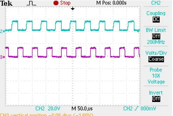
Figure 2: Drives of switch S1, S2 and S3, S4 and voltage waveform across transfer capacitor CT of the single
converter
The figure 2 shows the timing diagram of the boost SCC. The switch S1 and S2 is connected for the duration of time t1
now the transfer capacitor CT charges to VIN. After the time duration t1 the switch S1 and S2 is opened and the switch S3
and S4 is closed now CT discharges to the output voltage VO maintained across CO. CT is thus used to transfer energy
from the source to the load RL and to store energy in CO. The function of CO is to maintain VO within a small band of
III.EXPERIMENTAL RESULTS
A boost type switched capacitor DC-DC converter is implemented in the lab as shown in the figure 1. There are four mosfet’s and two capacitors in one converter model and two converter models is rigged up and the input is connected in parallel and output is measured in series. One converter model is tuned in such a way that input is 15volt and output is 14volt and same is done for the second model so the boost converter input is 15volt and output is 28volt
Table 1: Details of the mosfet’s used in the converter
MOSFET RDSON(ohm’s) IDSMAX(Amps)
S1 - P Channel (IRF 9630) 0.80 6.5
S2 – N Channel (IRO 7250) 0.11 26
S3 - N Channel (IRO 7391) 0.20 22
S4 - N Channel (IRO 7250) 0.11 26
S5 - P Channel (IRF 9630) 0.80 6.5
S6 – N Channel (IRO 7250) 0.11 26
S7- N Channel (IRO 7391) 0.20 22
S8 - N Channel (IRO 7250) 0.11 26
The transfer capacitor is a miniature aluminium electrolyte capacitor (Samwha SD capacitor) CT=3µF and output
capacitor is also a miniature aluminium electrolyte capacitor CO=33µF with very low ESR (equivalent series resistance).
VIN =15V and VO = 28V the input current IIN = 0.5A and output current is IO = 0.5A so the output power is 14watts.
The gate signals for the mosfet are driven by the PWM IC SG3524. The choice of selecting the capacitors is explained in [2]. The totem pole switches and the buffer circuits are used to drive the P-channel mosfet since the gate signals have to be inverted and the optocoupler IC 3120 is used to drive the N-channel mosfet and the optocoupler is powered by the voltage across the transfer capacitor CT.
Figure4: output voltage and output current waveform
Figure5: Hardware model of boost type switched capacitor converter
IV.CONCLUSION
The hardware model of SCC boost converter is realized with input VIN = 15V and VO = 28V which can deliver the
power of 14watts is tested in the open loop configuration. The switch drives, voltage and current waveform is presented in the paper.
ACKNOWLEDGEMENT
REFERENCES
[1] A. Ioinovici, “ Switched capacitor power electronic systems,” IEEE Magazine on circuit and systems, vol 1,issue 3, pp. 37-42, 2001
[2] P. K. Peter and V. Agarwal, “Analysis and design of a ground isolated switched capacitor DC-DC converter,” in Proc. IEEE Int. Symp. Ind. Electron., Bari, Italy, 2010, pp. 632–637.
[3] K. D. T. Ngo, and R. Webster, “Steady-state analysis and design of a switched-capacitor DC-DC converter,” IEEE Trans. Aerosp. Electron.Syst., Vol. 3, pp. 92–101, Jan. 1994.