„
…
2„
…
Si–N–SiO
2, and
„
c
…
SiC–SiO
2interfaces
G. Lucovskya)
Department of Physics, Department of Materials Science and Engineering, and Department of Electrical and Computer Engineering, North Carolina State University, Raleigh, North Carolina 27695-8202
H. Yang
Department of Chemistry, North Carolina State University, Raleigh, North Carolina 27695-8204
H. Z. Massoud
Department of Electrical Engineering, Duke University, Durham, North Carolina 27708-0291
~Received 21 January 1998; accepted 21 May 1998!
This article identifies procedures to calculate charge-transfer dipoles at semiconductor–dielectric interfaces, focusing primarily on the Si–SiO2system. Since SiO2is more polar than Si, there is a transfer of electrons from Si to SiO2 to balance the difference in chemical potentials creating a dipole localized at the semiconductor–dielectric interface. This dipole increases the conduction-band offset energy difference between Si and SiO2, and therefore, has important effects on interface electrical and optical properties. Empirical chemistry and ab initio methods have been applied to molecular clusters which emulate the interface bonding, and have been used to calculate interfacial charge transfer at~i! abrupt Si–SiO2 interfaces and~ii!nitrided Si–N–SiO2 interfaces. Additional calculations have applied to determine the average dipoles at Si–SiO2 interfaces with suboxide bonding in excess of the monolayer level required to form an ideal interface. The calculations support experimental data that indicate that the effective conduction-band offset energies at nitrided Si–N–SiO2 interfaces and at interfaces with minimized suboxide bonding are essentially the same. Finally, the calculations have been extended to SiC–SiO2 interfaces to illustrate the effects of changing from a homopolar to a more ionic or heteropolar semiconductor. © 1998 American Vacuum Society.@S0734-211X~98!07604-5#
I. INTRODUCTION
The energy difference ~or offset!between the conduction bands of crystalline Si and the SiO2gate dielectric in metal– oxide–semiconductor ~MOS! field-effect transistors ~FETs! plays a significant role in determining many optical and elec-trical properties including the barrier heights for internal photoemission and electrical tunneling, and the threshold voltages which define the onset of current flow in n-channel FETs. Similar considerations also apply for the valence-band offset energies. As FET device dimensions shrink in the deep submicron ~e.g., channel lengths ,0.15 mm!, the oxide equivalent thickness of gate dielectrics must be reduced pro-portionally to less than 3 nm, a thickness regime in which direct tunneling can play a significant role in the off-state leakage current.1 Benefits of nitridation of ultrathin oxides have been identified, and include~i!decreased defect genera-tion under accelerated stress bias testing, ~ii! decreased Fowler–Nordheim and direct tunneling currents, and ~iii! containment of boron penetration out of heavily doped p1 polycrystalline gate electrodes.2–4 The first two improve-ments are associated with interface nitridation at the mono-layer level,2,3 whereas the third is optimized by plasma-assisted top surface nitridation,3or the use of stacked oxide-nitride ~ON! dual-layer dielectrics.4 This article addresses
one aspect of interface nitridation by comparing charge-transfer dipoles at nitrided and non-nitrided Si–SiO2 inter-faces.
The driving force for the charge-transfer process underly-ing the results of this article was identified more than ten years ago.5–7At that time, it was shown that equalization of the chemical potential across the interface layer was respon-sible for interfacial charge transfer. The chemical-potential equalization process was quantified using an empirical ap-proach by applying the principal of electronegativity equal-ization as formulated by Sanderson.8–10 The motivation for the analysis in Ref. 7 was to explain differences in the sign of the valence-band offset energies for Si–SiO2 interfaces that had been hydrogenated or cesiated. The motivation in Refs. 8 and 9 was to explain differences between flatband voltages at Si~111!–SiO2 and Si~100!–SiO2 interfaces. The major contribution of this article is to go significantly beyond the zeroth-order model calculations of Refs. 7–9, and de-velop a more quantitative approach that could be applied to
~i! nitrided Si–N–SiO2 interfaces, ~ii! Si–SiO2 interfaces with suboxide transition regions, as well as ~iii! other semi-conductor dielectric interfaces such as SiC–SiO2. In addi-tion, the success of this model in addressing nitrided Si–N–SiO2and Si–SiO2interfaces with suboxide transition regions has provided an important perspective with respect to the different roles that interface nitridation and suboxide transitions regions play in strain relief at Si–SiO2interfaces.
a!
The approach of Refs. 8–10 is reviewed to provide a background for development of the calculations of this ar-ticle. The Sanderson electronegativity approach uses an em-pirically based method for determining charge transfer be-tween near-neighbor atoms with different electro-negativities.8–10 Figure 1 indicates the simplified structural model of Refs. 6 and 7 as it was first applied to abrupt Si~111!–SiO2 interfaces. The calculation of the charge-transfer dipole was performed at a molecular level where the two molecular constituents were the Si atoms of the crystal-line substrate and SiO2pseudoatoms of the oxide layer. The driving force for interfacial charge transfer is the electrone-gativity equalization principle of Refs. 8–10. If SA is the
electronegativity of one atom of a diatomic molecule AB, and SBthe electronegativity of the other atom, then charge is
transferred between A and B until they reach the same elec-tronegativity or chemical potential. A geometric mean is used to define electronegativity equalization, so that if SA* and SB* are the equalized atomic electronegativities after charge transfer has occurred, then SA*5SB*5(SA3SB)0.5.
This approach has been extended to larger molecules in which the atoms have additional nearest, and/or more distant neighbors.11Once the values of SA*and SB* have been deter-mined, partial charges on A and B, epA, and epB,
respec-tively, can be calculated using an empirical relationship de-veloped in Refs. 8–10,
epA5~SA*2SA!/0.83SA
0.5
and
epB5~SB*2SB!/20.83SB
0.5
, ~1!
where the normalization constant in the denominator is based on an assumed ionicity of 75% for the NaF molecule. If A has lower electronegativity, the partial charge of A is positive and the partial charge of B is negative, indicating a direction of charge transfer consistent with the definition of electrone-gativity as first proposed by Pauling.12
Applying the diatomic molecule model to the Si–SiO2 interface in Fig. 1, the renormalized electronegativities after chemical-potential equalization are 3.85 for both Si and
SiO2, yielding partial charges of10.18 e for Si and20.18 e for SiO2. If a less ‘‘electronegative’’ dielectric such as Si3N4 is substituted for SiO2, then the renormalized electronega-tivities are smaller, leading to reduced partial charges of
10.11 for Si and20.11 for Si3N4. Applied to Si–SiO2 in-terfaces in MOS structures, the molecular model of Refs. 6 and 7 has yielded charge-transfer dipoles that account for differences in flatband voltages reported for MOS devices on Si~100! and Si~111! substrates.6,7 In Refs. 6 and 7 a road map was presented for extending the electronegativity equal-ization approach to more complicated interfaces such as those that include interfacial nitridation, and/or interfacial suboxide bonding. This article follows that road map and focuses on interfacial bonding issues that have emerged as being important at Si–SiO2 interfaces with ultrathin oxide dielectrics and nitrided interfaces.
II. CALCULATIONS OF CHARGE-TRANSFER INTERFACE DIPOLES
Charge-transfer dipoles are calculated in two different ways in this article: ~i! by applying the empirical chemical method of Refs. 5–7 to larger clusters, which include the effects of more distant neighbors in a manner consistent with the approaches previously developed for large molecules11,13 and disordered networks;14,15 and ~ii! by using hydrogen-terminated molecular clusters as discussed in Ref. 16. These results are then compared in Table I with the results calcu-lated from the ‘‘pseudomolecule’’ approach of Refs. 6 and 7. In order to make these comparisons, it was necessary to ex-tend the approach of Refs. 6 and 7 to include monolayer interface nitridation and suboxide transition regions. For the nitrided interface, the ‘‘pseudomolecule’’ that was used to replace SiO2in Fig. 1 was characterized by the average elec-tronegativity of SiO2 and Si3N4, 3.63. This gives a Si-atom partial charge of 0.15 e, as compared to 0.18 e for the Si–SiO2interface. Similarly, for the interface with a subox-FIG. 1. Molecular model for abrupt interfaces between Si~111!and SiO2
‘‘atoms.’’
TABLEI. Calculated charges, dipole moments, and dipole potential steps for
Si~111!interfaces.
Interface bonding
Partial charge on Si60.01 (e)
Dipole moment
60.01 (e3Å)
Potential step
60.01~eV! ~a!Abrupt Si–SiO2
Two-layer 0.18 0.29 0.54 Empirical cluster 0.23 0.37 0.67
Ab initio cluster 0.22 0.36 0.68
~b!Nitrided Si–N–SiO2
Two-layer 0.15 0.26 0.48 Empirical cluster 0.18 0.31 0.57
Ab initio cluster 0.18 0.36 0.65
~c!Si–SiOx– SiO2
Two-layer 0.16 0.25 0.47 Empirical cluster 0.17 0.28 0.52
Ab initio cluster 0.18 0.29 0.54
~d!Abrupt Si–Si3O4
ide transition region, the ‘‘pseudomolecule’’ that was used to replace SiO2in Fig. 1 was characterized by the average elec-tronegativity of SiO2and SiO, 3.85, yielding a Si-atom par-tial charge of 0.16 e. Since the Si–N bond length is about 7% larger than the Si–O, this calculation gives essentially equal interfacial dipole moments of about 0.25 e Å.
Consider next the empirical chemical approach. As noted above, the computational basis for including near-nearest-and more-remote-neighbor chemical induction effects in molecules was first developed by Carver and Gray.11 This was subsequently extended by Lucovsky and co-workers to network amorphous solids.14,15Using the method of Ref. 14, the interface between crystalline Si oriented in a~111! direc-tion, and noncrystalline SiO2is represented by the molecular cluster in Fig. 2~a!. The Si side of the cluster consists of a three atomic shells~two are shown in the diagram!:~i!the Si atom at the interface in shell ~1!, ~ii! the three nearest-neighbor Si atoms in shell~2!, and~iii!nine pseudoatoms in shell ~3!, which are characterized by the average electrone-gativity of the rest of the network. A similar construction is used for the SiO2network on the other side of the interface. In this case, the cluster contains atomic shells of alternating Si and O atoms, as well as a final shell that is comprised of pseudoatoms with the average electronegativity of the SiO2 network (Saverage5@(SSi)(SiO)2#1/354.26). A similar cluster has been used for the ab initio calculations, except that the terminating species are hydrogen atoms rather than pseudoa-toms with average properties. The cluster used for empirical calculations as applied to abrupt nitrided Si–N–SiO2 inter-faces is shown in Fig. 2~b!. It is not possible to characterize suboxide bonding by a single representative cluster. In order to illustrate the effects of suboxide bonding it is, therefore, reasonable to average over two clusters that emulate an av-erage SiO composition. This is done by combining the clus-ter in Fig. 2~a! for the idealized Si–SiO2 interface with the cluster in Fig. 2~c!, which effectively extends the Si substrate into oxide and increases the coordination of the interface Si atom of the substrate with oxygen atoms from one to three. Total energy ab initio calculations were performed using a many-electron embedding theory that permits accurate computation of molecule–solid-surface interactions. Calcula-tions were carried out at an ab initio configuration interaction
~CI!level, in which all electron–electron interactions are ex-plicitly calculated and there are no exchange approximations or empirical parameters. The details of the method are exten-sively discussed in Refs. 17–19. The ab initio calculations are performed by first obtaining self-consistent-field ~SCF! solutions for the H-atom-terminated dielectric and Si sub-strate clusters. The occupied and virtual orbitals of the SCF solution are then transformed separately to obtain orbitals spatially localized within the bonds of the dielectric cluster and the Si substrate. This unitary transformation of orbitals, which is based upon exchange maximization with atomic valence orbitals, enhances convergence of the configuration interaction expansion.17–19
III. RESULTS
Table I includes the results of the three calculations de-scribed above. Presented in Table I are:~i!the partial charge on the substrate Si atom,~ii!the charge-transfer dipole, and
~iii!the calculated potential step at the interface. The poten-tial stepDV was obtained using the approach of Refs. 6 and 7, i.e.,
FIG. 2. Cluster model for Si–dielectric interfaces:~a!abrupt Si~111!–SiO2,
~b!abrupt nitrided Si~111!–N–SiO2, and~c!Si~111!–SiO2with interfacial
DV5@epSi3ld3NSi~111!3sinF/~eAV!#, ~2!
where ldis the atomic separation between the Si atom of the
substrate and the first atomic shell of the dielectric, NSi(111) is the areal density of Si atoms on a Si~111!surface,Fthe angle between the substrate Si-atom bond and the interface, and eAV is an average dielectric constant, e.g., eAV5(eSi
1eSiO2)/257.75.
Consider first the abrupt Si~111!–SiO2interface. The em-pirical two-layer molecular model of Refs. 6 and 7 gives values of epSi and DV that are smaller, respectively, than those obtained by the cluster calculations approaches. In ad-dition, the value ofDV is less than that given in Refs. 6 and 7 due to the assumption of different charge separation dipole distances. In the calculations of this article, a nominal Si–O bond length of 0.162 nm ~1.62 A! was used, whereas the calculations of Refs. 6 and 7 employed a larger value that was estimated from the covalent bonding radius of Si and the ‘‘size’’ of a SiO2‘‘molecule.’’ More importantly, the empiri-cal empiri-calculations and the ab initio empiri-calculations based on the cluster structures of this article @see Fig. 2~a!# give essen-tially the same results for the partial charge and the interface potential step at abrupt Si–SiO2interfaces. For the empirical calculation, the nominal dipole length of 0.162 nm was used in calculating DV, whereas for the ab initio approach, the
;3% larger relaxed Si–O bond length of the energy optimi-zation calculation was used. Based on an electron energy representation of the interface band structure, the direction of the dipole increases the potential step at the conduction-band discontinuity between the Si~111! substrate and the SiO2 conduction band. This would lead to negative shifts of the flatband and threshold voltages in MOS devices.6,7
Similar results were obtained using the cluster in Fig. 2~b! for an abrupt N-atom-terminated interface Si–N–SiO2. As displayed in Table I, the diatomic molecular model of Refs. 6 and 7 gives values of epSi andDV that are again smaller than those obtained by the cluster calculations of this article. However, as the case of the Si–SiO2 calculations, the em-pirical and ab initio calculations based on the cluster model of this article give essentially the same results for the partial charge and the interface potential steps. The difference be-tween the nominal Si–N bond length of 0.174 nm, and the one obtained in the ab initio calculation accounts for the differences inDV between these calculations. The significant result of these calculations on nitrided Si–SiO2interfaces is that the partial charge on the Si atom of the substrate is reduced by the interposition of a N atoms at Si–SiO2 inter-faces, and that this leads to a small reduction of the interface potential step of approximately 0.1 eV with respect to non-nitrided abrupt Si–SiO2interfaces. To confirm the trends in
epSi andDV for interface nitridation, calculations based on
the molecular model of Refs. 6 and 7, and the empirical cluster model of this article were performed for a Si~111!–Si3N4 interface, and these have also been included in Table I. These calculations support the differences ob-tained for the abrupt Si~111!–SiO2 and nitrided Si~111!–N–SiO2interfaces, since increased nitridation leads
to smaller interfacial dipoles with correspondingly smaller contributions to the conduction-band offset energies.
Finally, Table I includes the results of calculations for Si~111!–SiOx– SiO2 interfaces with suboxide transitions re-gions. Different degrees of suboxide bonding have been ap-proximated by placing a Si atom in the first shell of the dielectric and then increasing the number of Si atoms in the second shell bonded to that atom@see Fig. 2~c!#. As the num-ber of Si atoms in the second shell increases, the partial charge on the Si atom of the substrate decreases, and the potential step contributionDV also decreases proportionally. However, the ab initio calculation for this type of interface was performed for the cluster with only one layer of subox-ide bonding with no additional Si atoms attached to the Si atom of the first shell of the transition region. For purposes of comparison, the entries into Table I for the interface with suboxide bonding, Si~111!–SiOx– SiO2, are the average of the results obtained for the clusters in Figs. 2~a!and 2~c!.
The charge transfer interface dipole has been calculated as a function of the interatomic distance of the interface atoms, i.e., the Si–O distance as in Fig. 2~a!, Si–N distance as in Fig. 2~b!, and Si–Si distance as in Fig. 2~c!, and these results are presented in Figs. 3~a!, 3~b!, and 3~c!. The results in Figs. 3~a!and 3~b! for the clusters of Figs. 2~a!and 2~b!, respec-tively, demonstrate that the charge-transfer dipole decreases approximately linearly with increasing interatomic distance for the abrupt Si–SiO2 and nitrided Si–N–SiO2 interfaces. This dependence of the charge-transfer dipoles requires that the partial charge on the Si atom decrease approximately quadradically with increasing interatomic spacing for the range of the interfacial bond lengths explored. In contrast and as shown in Fig. 3~c!, the variation of the charge-transfer dipole with interface bond length is reversed for the cluster that is used to emulate suboxide bonding so that the dipole increases with increasing Si–Si separation. Analysis of this dependence shows that it is a direct consequence of compe-tition between two different contributions to the interface dipole. One contribution comes from a dipole between the Si substrate atom and the Si atom of the first shell of the dielec-tric that is directed toward the Si substrate, and the second contribution that is oppositely directed comes from the atoms of the second and third shells of the dielectric. The net effect of these two contributions is to give an effective interfacial dipole that is significantly smaller than that of an abrupt Si~111!–SiO2interface. This explanation is supported in Fig. 3~c!by an additional observation that shows that as the Si–Si distance is increased out of a linear regime the value of the interfacial charge-transfer dipole approaches the value of the dipole expected for a Si–SiO2 bonding arrangement.
dielectric, and the decrease in the potential step is due to the bonding geometry. In particular, the sinFfactor is reduced from 1 to 0.577 as the projection angle of the dipole onto a normal to the plane of the interface decreases from 90° to 35.25°.
Table III presents the results of empirical cluster calcula-tions for SiC~0001!–SiO2 interfaces. The major difference between the calculated partial charges on the Si atom on the SiC~0001!substrate and on the Si~111!substrate are driven by the heteropolar character of the SiC semiconductor. The increased polar character of the SiC substrate reduces the partial charge on the Si surface atom relative that of the Si~111!substrate.
IV. DISCUSSION
This section addresses several different aspects of the cal-culations of Sec. III including ~i! development of a band model for the Si–SiO2interface that takes into account dif-ferences due to interface nitridation, and interfacial suboxide regions; ~ii! the comparison of these calculations with ex-perimental results for Si–SiO2interfaces; and~iii!a perspec-tive for semiconductor dielectric interfaces that parallels a
framework established for lattice-mismatched
semiconductor–semiconductor heterointerfaces.
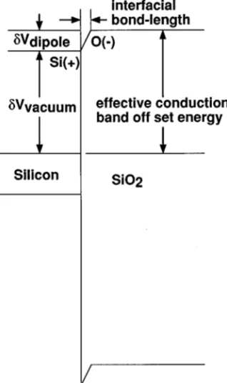
A. Band model for Si–SiO2interfaces
Figure 4 presents a band model for the conduction- and valence-band offset energies between Si and SiO2. As shown in the diagram, there are two contributions to the conduction-band ~and therefore, also the valence-band! potential steps:
~i! the first comes from differences between the potential steps of the respective interface components relative to
FIG. 3. Interface dipole as a function of interface bonding distance from the abate calculations: ~a! abrupt Si~111!–SiO2, ~b! abrupt nitrided
Si~111!–N–SiO2, and~c!Si~111!–SiO2, with interfacial transition region
with suboxide transition. The solid lines in~a!and~b!are a linear fit to the calculated data points; the solid line in~c!is a smooth fit to the calculated data points.
TABLEII. Calculated charges, dipole moments, and dipole potential steps for
Si~100!interfaces.
Interface bonding
Partial charge on Si60.01 (e)
Dipole moment
60.01 (e3Å)
Potential step
60.03~eV! ~a!Abrupt Si–SiO2
Empirical cluster 0.32 0.28 0.46
~b!Nitrided Si–N–SiO2
Empirical cluster 0.26 0.26 0.41
~c!Si–SiOx– SiO2
Empirical cluster 0.21 0.24 0.38
TABLEIII. Comparisons of partial charges on Si interface atoms between Si~111!and Si-atom terminated SiC~0001!interfaces.
Partial charge on Si
Interface bonding
Si~111!
60.01 (e)
SiC~0001!
60.01 (e) ~a!Abrupt Si–SiO2
Two-layer 0.18 0.13
Empirical cluster 0.23 0.17
~b!Nitrided Si–N–SiO2
Two-layer 0.15 0.10
Empirical cluster 0.18 0.12
~c!Si–Si3N4
Two-layer 0.11 0.06
vacuum, and ~ii! the second comes from the interfacial di-poles of this article. DiMaria and co-workers performed in-ternal photoemission measurements to determine the conduction-band potential steps between Si and SiO2 ~Ref. 20! and Si and Si3N4,
21
and these values have been used extensively in characterizing interface properties, as for ex-ample, in calculations of direct tunneling currents.22 The re-sults of this article indicate that care must be taken in apply-ing these nominal conduction-band offset potential-energy steps. For example, the calculations of this article have dem-onstrated significant differences in effective conduction-band offset energies that depend on the local atomic bonding at the interface, including both interface nitridation, and transi-tion regions with suboxide bonding.
B. Comparison with experiments
The calculations of this article are now compared with results of several different experimental studies. First, a word of caution regarding such comparisons. There are two factors involved in interface formation that contribute to differences in interfacial bonding arrangements of the types discussed in this article: ~i! the process, or process steps by which the interface is formed, as for example, thermal oxidation, plasma-assisted oxidation, plasma-assisted oxidation com-bined with post-oxidation nitridation, etc., and~ii!the chemi-cal and structural interfacial relaxations associated with post-formation rapid thermal annealing ~RTA!, or downstream thermal exposures. The combination of these two interface fabrication effects is illustrated by results obtained from
op-tical second-harmonic-generation ~SHG! experiments on vicinal Si~111!–SiO2interfaces,23–25which are presented in Table IV.
The experimental approach and the data reduction proce-dures for the optical SHG studies are described in detail in Refs. 23 and 24. The columns in Table IV labeled A1/A3 andDF13, which are obtained from a harmonic analysis of angular anisotropy measurements in vicinal Si~111!surfaces and reflect differences in interface bonding as a function of the two processing factors identified above. The SHG re-sponse is dominated by the Si–SiO2interface for the polar-izations of the incident and reflected optical waves atvand 2v, respectively. Combined with the results presented in Ref. 26, which demonstrate significant reductions in interfacial transition regions following a 30 s 900 °C RTA in a chemi-cally inert ambient such as Ar or He, the SHG results in Table IV demonstrate that interfaces formed by thermal oxi-dation at temperatures below 850 °C, and remote plasma-assisted oxidation/nitridation at 300 °C, display the same val-ues of A1/A3 andDF13, and are essentially the same with suboxide transition regions being the determinant factor in determining interface properties. After the anneal, the non-nitrided interfaces formed by either thermal or remote plasma-assisted oxidation are essentially the same, but are different from the interfaces that contain approximately 1 monolayer~ML!of interface nitridation. X-ray photoelectron spectroscopy ~XPS! studies on non-nitrided interfaces have established that ~i!there is a reduction of suboxide bonding following the 30 s 900 °C RTA for non-nitrided interfaces formed by both thermal and plasma-assisted oxidation, and
~ii! following the RTA, there is still measurable suboxide bonding ;1.5 excess monolayer equivalents of suboxide bonded Si atoms, as opposed to approximately 3 ML equiva-lents before RTA.27
In the examples that are discussed below, the Si–SiO2 interfaces were subjected to a 30 s 900 °C RTA so that com-parisons between the calculations and experiment will utilize the results of the ab initio calculations for the abrupt nitrided Si–SiO2, and the interface with the smallest amount of sub-FIG. 4. Band model for Si–SiO2interfaces show interface potential due to
charge-transfer dipoles.
TABLE IV. Summary of results from studies of vicinal Si~111!surfaces
off-cut;5° in the 112 bar direction.
~a!Surface treatment—plasma processinga
Phase:DF13
62°
A1/A3
60.03
O2, 15 s, 300 °C 68 0.20
O2, 15 s, 30 s 900 °C RTA (0.5%O2/Ar)b 23 0.35
N2O, 15 s, 300 °C 67 0.21
N2O, 15 s, 30 s 900 °C RTA~Ar! 11 0.37
N2O, 30 s, 300 °C 65 0.17
N2O, 30 s, 30 s 900 °C RTA~Ar!b 11 0.35
~b!Surface treatment—thermally grown interfaces
Furnace oxidation at 850 °C 72 0.19 Postoxidation anneal
~30 s at 950 °C (0.5%O2/Ar)
23 0.33
oxide bonding. The interfaces characterized by optical SHG have been prepared on Si~111!surfaces, where as those dis-cussed below for MOS devices were formed on Si~100! sub-strates. It was established earlier in Tables I and II that quali-tative trends in interface potential steps as a function of interface bonding are the same for Si~111!and Si~100! inter-faces. The differences are in the quantitative aspects of the calculations, namely, the magnitudes of theDVs, and differ-ences in these values for different interface bonding on Si~111! and Si~100!substrates are small and within the ex-perimental uncertainties of the exex-perimental data.
It is tempting to compare the results of these calculations with barrier heights used to interpret tunneling studies on MOS devices with ultrathin gate dielectrics; however, the extraction of effective barrier heights from tunneling data is not unambiguous. For example, it depends on assumptions made about the magnitude of the effective mass of the tun-neling electrons, and approximations made taking into ac-count potential drops in the substrate and polycrystalline gate electrodes.22 The results presented in Ref. 28 demonstrate that tunneling current densities are markedly different for nitrided and non-nitrided interfaces with nitrided interfaces showing reductions in tunneling current that are independent of the direction of the injection, substrate, or gate, and that are also quantitatively the same for tunneling in the Fowler– Nordheim~5 nm!and direct tunneling~2 and 3 nm!regimes. However, since the flatband voltages vary by no more than 0.05 eV, the reductions in tunneling current are not due to deferences in barrier heights at the substrate–Si/dielectric layer interface. Since the samples in Ref. 28 were subjected to postdeposition annealing in inert ambients at 900 °C, this leads us to conclude that the effective barrier heights at struc-turally and chemical relaxed, nitrided, and non-nitrided inter-faces are essentially the same. This suggests that the effec-tive barrier height at Si–SiO2 interfaces with minimal suboxide bonding is essentially the same are for a fully ni-trided interface. This result is consistent with the calculations presented in Tables I and II. The agreement between the predictions of the calculation and the tunneling experiments validates the average bonding model used for the interfaces with minimal suboxide bonding.
C. Stress relief at Si–SiO2interfaces
The results presented in this article, and in particular, the good agreement between the calculations and the tunneling experiments provide an important insight into the issue of the different roles of suboxide bonding and interface nitridation in stress relief at Si–SiO2interfaces. There is a large molar volume mismatch between Si and SiO2 that means that the effective spacing of Si atoms in these two materials is mark-edly different. The Si–Si bond length in crystalline Si is 0.235 nm ~2.35 A!, whereas the second-nearest-neighbor Si–Si distance in SiO2is 0.30560.005 nm (3.0560.05 Å). The large mismatch in interatomic distances means that the Si–SiO2 interface is in many respects an analog of lattice-mismatched semiconductor heterointerfaces. The formation of non-lattice-matched semiconductor heterointerfaces is
ac-complished in several different ways: ~i!by pseudomorphic growth habits, where there are large strains in the epitaxial overgrowth layer and wherein the maximum thickness of the pseudomorphic overgrowth is inversely proportional to the strain;~ii!by the formation of interface defects in the form of dislocations; and~iii!by reduction of interface strain through the use of buffer layers with intermediate values of lattice constants.
The formation of non-nitrided Si–SiO2interfaces requires a transition region with suboxide bonding to reduce the very large strain mismatch between the Si and the SiO2. From the XPS studies, it can be concluded that the minimum suboxide bonding region after postoxidation annealing at 900 °C con-tains about 1.5 ML of Si.27 The incorporation of interfacial nitrogen at the monolayer level is an analog of the buffer layer approach, where a material with a different composi-tion can accommodate a significant fraccomposi-tion of the strain mis-match and thereby reduce the strain and require reduced sub-oxide bonding.
V. SUMMARY
In summary, this article has demonstrated that interfacial transition regions at non-nitrided Si–SiO2 interfaces reduce the partial charge of Si atoms on the Si side of that interface, thereby reducing the interfacial charge-transfer dipole below the value it would have for an abrupt Si–SiO2interface with no suboxide bonding beyond what is required to define the interface. Monolayer concentrations of nitrogen atoms incor-porated at Si–SiO2 interfaces have a similar effect in the context that they also reduce the partial charge on the Si atoms on the Si side of the interface below the value it would have had at an abrupt Si–SiO2interface. The model calcula-tions based on empirical chemistry and ab initio approaches applied to the same interface cluster models, combined with the two-layer molecular approach indicate the conduction-band offset between Si and SiO2is only slightly increased by monolayer nitrogen-atom incorporation as compared to mini-mal suboxide bonding. For Si~111!interfaces, the calculated average difference in interfacial conduction-band offsets, dDV, is estimated to be 0.0560.03 eV. Similar differences are obtained for Si~100!interfaces using the empirical cluster model. The results of recent experiments on tunneling cur-rents in fully nitrided Si~100!–SiO2 interfaces are in accord with the predictions of these calculations. The reduction in tunneling currents for nitrided interfaces reported in Ref. 29 must then be attributed to other factors including, for ex-ample, reductions in interface roughness that accompany in-terfacial nitridation.
ACKNOWLEDGMENTS
This research is supported by the Office of Naval Re-search~ONR!, the National Science Foundation~NSF! Engi-neering Research Center~ERC!at North Carolina State Uni-versity ~NCSU!, and the Semiconductor Research Corporation ~SRC!.
1D. Buchanan, J. Vac. Sci. Technol. B~to be published!.
2D. R. Lee, G. Lucovsky, M. R. Denker, and C. Magee, J. Vac. Sci.
Technol. A 13, 1671~1995!; D. R. Lee, C. R. Parker, J. R. Hauser, and G. Lucovsky, J. Vac. Sci. Technol. B 13, 1778~1995!.
3S. V. Hattangady et al., Tech. Dig. Int. Electron Devices Meet., 495
~1996!.
4Y. Wu, G. Lucovsky, and H. Z. Massoud, in Proc. IEEE Reliability Phys.
Symp.~1998!.
5P. Perfetti, C. Quaresima, C. Coluzza, C. Fortunato, and G. Margaritondo,
Phys. Rev. Lett. 57, 2065~1986!.
6H. Z. Massoud, Mater. Res. Soc. Symp. Proc. 105, 265~1988!. 7H. Z. Massoud, J. Appl. Phys. 63, 2000~1988!.
8R. T. Sanderson, Chemical Periodicity~Van Nostrand Reinhold,
Prince-ton, NJ, 1960!.
9R. T. Sanderson, Inorganic Chemistry~Reinhold, New York, 1967!. 10R. T. Sanderson, Chemical Bonds and Bond Energy, 2nd ed.~Academic,
New York, 1976!.
11J. C. Carver, R. C. Gray, and D. M. Hercules, J. Am. Chem. Soc. 96,
6851~1984!.
12L. Pauling, The Nature of the Chemical Bond, 3rd. ed.~Cornell University
Press, Ithaca, NY, 1960!.
13G. Lucovsky, Solid State Commun. 29, 571~1979!. 14
D. V. Tsu, B. N. Davidson, and G. Lucovsky, Phys. Rev. B 40, 1795 ~1989!.
15
G. N. Parsons and G. Lucovsky, Phys. Rev. B 41, 1664~1990!.
16
Z. Jing, G. Lucovsky, and J. L. Whitten, J. Vac. Sci. Technol. B 13, 1613 ~1995!.
17
P. Cremaschi and J. L. Whitten, Theor. Chim. Acta 72, 485~1987!.
18
J. L. Whitten and H. Yang, Int. J. Quantum Chem., Quantum Chem. Symp. 29, 41~1995!.
19J. L. Whitten and H. Yang, Surf. Sci. Rep. 24, 55~1996!. 20D. J. DiMaria, J. Appl. Phys. 50, 5826~1979!.
21D. J. DiMaria~private communication!.
22H. Y. Yang, H. Niimi, and G. Lucovsky, J. Appl. Phys. 83, 2327
~1998!.
23C. H. Bjorkman, T. Yasuda, C. E. Shearon, Jr., U. Emmerichs, C. Meyer,
K. Leo, and H. Kurz, J. Vac. Sci. Technol. B 11, 1521~1993!.
24C. H. Bjorkman, C. E. Shearon, Jr., Y. Ma, T. Yasuda, G. Lucovsky, U.
Emmerichs, C. Meyer, K. Leo, and H. Kurz, J. Vac. Sci. Technol. A 11, 964~1993!.
25
U. Emmerichs, C. Meyer, H. J. Bakker, F. Wolter, H. Kurz, G. Lucovsky, C. Bjorkman, T. Yasuda, Yi Ma, Z. Jing, and J. L. Whitten, J. Vac. Sci. Technol. B 12, 2484~1994!.
26G. Lucovsky, A. Banerjee, B. Hinds, B. Claflin, K. Koh, and H. Yang, J.
Vac. Sci. Technol. B 15, 1074~1997!.
27
J. Rowe~unpublished!.
28
G. Lucovsky, H. Niimi, Y. Wu, C. G. Parker, and J. R. Hauser, J. Vac. Sci. Technol. A 16, 172~1998!.
29C. H. Bjorkman, J. T. Fitch, and G. Lucovsky, Appl. Phys. Lett. 56, 1983
~1990!.
30