A Review onDesign of a high gain Microstrip
Antenna using Parasitic Patch for GPS
Application
RupeshBudharam Raut
1, Prof. V. D. Nagrale
2Dept. of Electronics, AISSMS‟s COE, Savitribai Phule Pune University, Pune, Maharashtra, India1
Dept. of Electronics, AISSMS‟s COE, Savitribai Phule Pune University, Pune, Maharashtra, India2
ABSTRACT: GPS patch antennas are gaining their importance nowadays due to their importance in the communication engineering. This paper proposes a novel approach to increase the gain of microstripantenna.The application of gap-coupled mechanism for achieving high gain with microstrip antenna has been proposed .This present work includes the designing of patch antenna for the applications of Global positioning systems antenna in the handheld equipment. The antenna will operate at the desired frequency of 1.57GHz with 80 MHz bandwidth. An FR4 substrate of dielectric constant 4.4 and dielectric loss tangent of 0.027 is used in this present work. The proposed antenna possesses an average gain of 4.0 dB overall the GPS L1 operation. Return loss, input impedance smith chart, 3D gain, radiation patterns and field distributions are simulated and presented in this paper by using commercial Ansoft-HFSS software.
KEYWORDS: GPS (Global positioning systems), Patch antenna, parasitic patch, Electromagnetic coupling Microstrip Patch Antenna (ECMPA),
I. INTRODUCTION
Excitation of the microstrip antenna bya gap coupled mechanism appears to be a natural choice as the patch can be considered as an extension of the feed strip, and both can be simultaneously fabricated on the same plane, without much wastage of the substrate material. The gap-coupled capacitive feed strip requires a narrow gap width for efficient coupling of power. However,a narrow gap size will limit the power handling capability of the antenna[1]. A thicker substrate is generally preferred in the design of a microstrip antennabecause not only it is mechanically strong,but at the same time it provides increase radiated power, reduce conductor loss and improve bandwidth. The application of gap-coupled mechanism for achieving high gain and Bandwidht with microstrip antenna has been proposed.
The antenna will operate at the desired frequency of 1.57GHz with 80 MHz bandwidth.The proposed antenna configuration works well with conventional geometries such as rectangular and triangular patches and provides good impedance bandwidth.It also reduces spurious radiations. Further, by properly choosing the size of the feed strip and the separation distance between the feed strip and the driven patch, impedance bandwidth can be significantly improved up to 50%. The antenna design will simulate, teste and characterized by using Ansoft HFSS software.After fabrication the results can be measured and anlysed by netwokanalyzer.
A. Necessity:
GPS application requires high Bandwidth and high gain at low frequency. A coplanar parasitic patch can be used along the radiating edge of the driven patch to increase the bandwidth of rectangular patch. A variable distance between the patch ans parasitic element can be used forelectromagnetic coupling.
There are number of feedings techniques i.e. co-axial feed, proximity feed, aperature couple feed, microstrip feed, capacitive coupled feed etc toexicite MSA. I am using co-axial feed for the analysis as it is simple.
Design Rectangular Microstrip antenna (1.57Ghz) using parasitic element .
Changing parameters to improve drawbacks.
Changing air gap distance to increase efficiency of antenna.
Changing distance of patch to increase gain of antenna
Adding one more parasitic element to increase gain of antenna.
II. LITERATURESURVEY
S. Sarkar have presented the Design of a Compact Microstrip Antenna using Capacitive Feed and Parasitic Patch for Ultra-Wideband Application. The application of gap-coupled capacitive feeding mechanism for achieving UWB with microstrip antenna has also been proposed. The proposed antenna is capable of operating over a bandwidth (6.4GHz-10.4GHz). Although coaxial probe feed is one of the most popularly used feeding mechanism for thick substrates, but the inductance of the probe might create an impedance mismatch, which needs to be compensated by introducing a capacitive feed strip [1].
According to Pozar, the various bandwidth-enhancement techniques can be categorized into three broad approaches: impedance matching; the use of multiple resonances; and the use of lossy materials. It has been decided to rather categories the different approaches in terms of the antenna structures that are normally used. These include: wideband impedance-matching networks; edge-coupled patches; stacked elements; shaped probes; and finally capacitive coupling and slotted patches. In terms of Pozar‟s categories, all these approaches can be identified as making use of either impedance matching or multiple resonances [2].
Changrong Liu, Yong-XinGuo, and Shaoqiu Xiaopresented the, “Capacitive Loaded Circularly Polarized
Implantable Patch Antenna for ISM Band”. A single-fed miniaturized circularly polarized microstrip patch antenna is designed and experimentally demonstrated or industrial-scientific-medical (2.4–2.48 GHz) biomedical applications. The proposed antenna is designed by utilizing the capacitive loading on the radiator. Compared with the initial topology of the proposed antenna, the so-called square patch antenna with a center-square slot, the effect of coaxial cable is also discussed [3].
A new coplanar capacitively coupled feeding method for circularly polarized patch antenna is developed A prototype has been designed and simulated and found to have an impedance bandwidth of 5.3% and a 3 dB axial-ratio bandwidth of about 1.2% at the center frequency of 2250MHz. The coupling mechanism can be approximately considered as a microstrip coupled line directional coupler, which is simple and flexible to obtain circular polarization without any alteration to the microstrip radiator such as truncating the corner and add-on slits. This single-feed circular polarization could be achieved by only adjusting the microstrip feed lines, which is independent of the square patch radiator. The proposed capacitively coupled bandwidth such that is suitable for a wide range of circularly polarized microstrip antenna applications [4].
The effect of direct radiation from the open end of the microstrip line can be represented by a conductance across the shunt capacitor. In such kind of antenna configuration, the radiation pattern becomes asymmetric due to capacitive loading. To over-come this problem new feeding techniques are design[1].The two patches can be manufactured on a thin substrate with a thick low-loss substrate, such as air .The gap between the resonant patch and the capacitor patch acts as a series capacitor, thereby offsetting the inductance of the long probe. Once the size of the resonant patch and the thickness of the substrate have been fixed for a certain operating frequency and impedance bandwidth, there are basically two parameters that can be used to control the input impedance of the antenna element[7,9].
A. Effect Of Parasitic Patch:
III. ANTENNADESIGN
The three essential parameters for the design of a rectangular Microstrip Patch Antenna are:
A. Frequency of operation (fo): The resonant frequency of the antenna must be selected appropriately. The resonant
frequency selected for design is 1.57 GHz.
B. Dielectric constant of the substrate (ε r): The dielectric material selected for design is glass epoxy which has a
dielectric constant of 4.4.
C. Height of dielectric substrate (h): For the microstrip patch antenna to be used in cellular phones, it is essential that
the antenna is not bulky. Hence, the height of the dielectric substrate is selected as 1.6 mm.
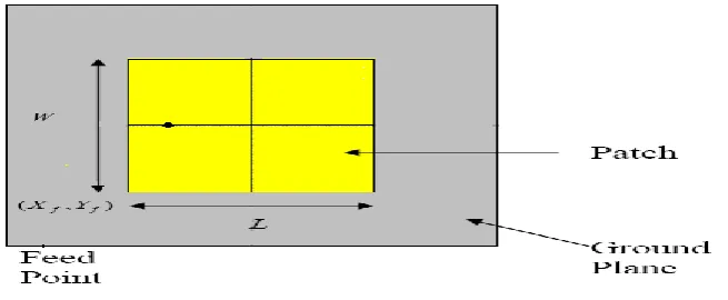
Figure 4.1: Rectangular microstrip antenna
The initial calculation starts from finding the width of the patch which is given as:
Step 1: Calculation of the width of Patch (W)
The width of the Microstrip patch antenna is given as
eq. (1)
Step 2: Calculation of effective dielectric constant.
Fringing makes the microstrip line look wider electrically compared to its physical dimensions.Since some of the waves travel in the substrate and some in air, an effective dielectric constant is introduced, given as:
eq. (2)
Where,
εreff= Effective dielectric constant εr= Dielectric constant of substrate
H = Height of dielectric substrate
W = Width of the patch
Step 3: Calculation of Length of Patch (L) The effective length due to fringing is given as:
eq. (3)
Due to fringing the dimension of the patch as increased by ΔL on both the sides, given by:
Hence the length of the patch is:
L= Leff-2ΔL eq. (5)
Step 5: Calculation of Substrate dimension For this design this substrate dimension would be
Ls=L+2*6h eq. (6)
Ws=W+2*6heq. (7) Step 6: Calculation of feed point
For this feed would be given L/4 distance.
IV. SOFTWAREREQUIREMENTS
A. Ansoft HFSS
It is Debian based linux operating system, HFSS is the industry standard simulation tool for 3D full wave elcctromaganectic field simulation.HFSS provides E and H fileld,current,S-parameter and near and far radiation filedsresults.Intrensic to the success of HFSS as an engineering design tool is its automated solution process where users are only required to specify geometry, material properties and the desired output.With the help of HFSS we can automatically generate an appropriate, efficient and accurate mesh for solving the problem.
V. RESULTSANALYSIS
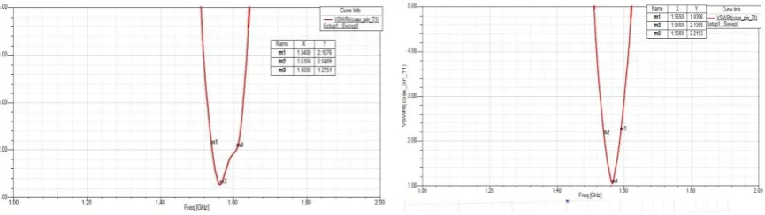
To achieve the performance of antenna, weadded two more parasitic patch element on primary antenna which provides a maximum both bandwidth & gain. The effects of with & without parasitic element near to radiating patch antennahasbeencarried out in Fig. 6.1 and fig 6.4.The value of VSWR at 1.57GHz frequency for simple microstrip antenna without parasitic patch is 1.03 and bandwidthis 45MHz.But at the same time when we will insert the parasitic patch on same substrate there is better electromagnetic coupling between parasitic patch and radiating element.Due to
this effect bandwidth will increase directly double i.e. 80 GHz and gain is also increased double up to 3.7 dB
.
A. VSWR:
The VSWR versus frequency of this antenna has been shown in fig.6.1 to 6.4. This antenna satisfies the bandwidth requirement of GPS system, i.e. from 1.52 to 1.57 GHz. Fig.6.4 indicate when we are adding parasitic path near to radiate patch then we get maximum bandwidth.
Fig 6.3:VSWR of rectangular microstrip antenna using Fig 6.4: VSWR of rectangular microstrip antenna using Parasitic patch on top side of radiating patch parasitic patch on both side of radiating patch
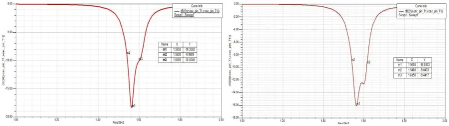
B. Return loss:
In order to see the effects of parasitic element on antenna‟s impedance characteristics, a parametric analysis has been carried out. From fig .6.4 to 6.8.and it indicate the two parasite patch near to antennagives maximum bandwidth near to 80MHz and return loss gives-16.02dB as shown in fig 6.8.
Fig 6.5:Return loss of Rectangular microstrip antenna Fig 6.6:Return loss of Rectangular microstrip antenna with parasitic patch on left side of rediating patch
Fig 6.7:Return loss of rectangular microstrip antenna using Fig 6.8:Return loss of rectangular microstrip antenna Parasitic patch on top side of radiating patch using parasitic patch on both side of radiating patch
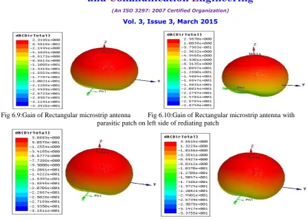
C. Gain:
Fig 6.9:Gain of Rectangular microstrip antenna Fig 6.10:Gain of Rectangular microstrip antenna with parasitic patch on left side of rediating patch
Fig 6.11:Gain of rectangular microstrip antenna using Fig 6.12: Gain of rectangular microstrip antenna using Parasitic patch on top side of radiating patch parasitic patch on both side of radiating patch
Table 6.1: Comparison table for different shapes in MSA
Sr.No Shape of Antenna Freq (GHZ)
Return Loss(dB)
VSWR Bandwidth
(MHZ)
Directivity (dB)
1. Rectangular MSA 1.56 -34.22 1.03 45 2.31
2. Rectangular parasitic top MSA
1.57 -33.88 1.04 48 2.98
3. Rectangular left parasitic MSA
1.56 -18.56 1.27 70 3.00
4. Rectangular double
parasitic MSA
1.56 -16.03 1.37 75 3.66
VI.CONCLUSION
REFERENCES
1. Kasabegoudar, V.G.; Vinoy, K.J., "Coplanar Capacitively Coupled Probe Fed Microstrip Antennas for Wideband Applications," Antennas and Propagation, IEEE Transactions on, vol.58, no.10, pp.3131, 3138, Oct. 2010.
2. S.Sarkar, “Design of a Compact Microstrip Antenna using Capacitive Feed and Parasitic Patch for Ultra-Wideband Application”, International Journal of Scientific and Research Publications, Volume 3, Issue 6, June 2013 1 ISSN 2250-315.
3. C. A. Balani , Antenna theory analysis and design, 3rd Edi.2005.
4. Changrong Liu; Yong-XinGuo; Shaoqiu Xiao, "Capacitively Loaded Circularly Polarized Implantable Patch Antenna for ISM Band Biomedical Applications," Antennas and Propagation, IEEE Transactions on, vol.62, no.5, pp.2407, 2417, May 2014.
5. Kunpeng Wei; Zhijun Zhang; Zhenghe Feng, "New coplanar capacitively coupled feeding method for circularly polarized patch antenna," Antennas and Propagation (APSURSI), 2011 IEEE International Symposium on, vol., no., pp.3099, 3102, 3-8 July 2011.
6. S. S. Yavalkar, R.T. dahatonde, Dr. S. S. Rathod and Dr. S.B. Deosrkar, „Comparative Analysis of BW enhancement of microstrip patch antenna using various geometry‟,IOSR-JECE sep-oct 2012.
7. Hao Wang; Jing Zhou; Yong Huang; Jie Wang, "Low-profile capacitive fed air-supported microstrip antenna at UHF band for biomedical application," Microwave Workshop Series on RF and Wireless Technologies for Biomedical and Healthcare Applications (IMWS-BIO), 2013 IEEE MTT-S International , vol., no., pp.1,3, 9-11 Dec. 2013.
8. Wenquan Cao; Bangning Zhang; Tongbin Yu; Hongbin Li, "A Single-Feed Broadband Circular Polarized Rectangular Microstrip Antenna With Chip-Resistor Loading," Antennas and Wireless Propagation Letters, IEEE , vol.9, no., pp.1065,1068, 2010.
9. Shiqiang Fu; Qinggong Kong; Shaojun Fang; Zhongbao Wang, "Broadband Circularly Polarized Microstrip Antenna with Coplanar Parasitic Ring Slot Patch for L-Band Satellite System Application," Antennas and Wireless Propagation Letters, IEEE , vol.13, no., pp.943,946, 2014.
10. Jiawei Dong; Anguo Wang; Peng Wang; YonghongHou, "A novel stacked wideband microstrip patch antenna with U-shaped parasitic elements," Antennas, Propagation and EM Theory, 2008. ISAPE 2008. 8th International Symposium on, vol., no., pp.185, 188, 2-5 Nov. 2008.
11. Oraizi, H.; Hamidkhani, M., "Wide-band microstrip patch antennas using parasitic elements and defected ground structures on different substrates," Antennas and Propagation (MECAP), 2010 IEEE Middle East Conference on , vol., no., pp.1,5, 20-22 Oct. 2010.
12. Singh, A.; Ansari, J.A.; Kamakshi, K.; Mishra, A.; Anessh, M., "Inset fed rectangular microstrip patch antenna with parasitic Element," Communications, Devices and Intelligent Systems (CODIS), 2012 International Conference on , vol., no., pp.549,551, 28-29 Dec. 2012. 13. Hang Wong; Kwok Kan So; Kwai Man Luk; Chi Hou Chan; QuanXue, "New size reduction for patch antenna by parasitic shorting
elements," Antenna Technology (iWAT), 2010 International Workshop on , vol., no., pp.1,4, 1-3 March 2010.
14. Dahlan, A.M.M.; Kamarudin, M.R., "Shorted patch antenna with parasitic elements," Microwave Conference, 2009. APMC 2009. Asia Pacific,Vol. No., pp.2653, 2655, 7-10 Dec. 2009.