ABSTRACT
LI, XIAOMIN. High Efficiency Integrated Switched Capacitor Converters for High Voltage Low Power Applications. (Under the direction of Dr. Alex Q. Huang).
This dissertation focuses on the topology analysis, efficiency enhancement design, and silicon implementation of an integrated Switched Capacitor DC-DC converter (SC-DCDC) for high voltage and low power applications. A new and comprehensive methodology for optimizing SC-DCDC based on the area constraint is proposed in this work. The optimization methodology identifies the relative sizes of each single capacitor and power switch device first. After that an optimized ratio between the total capacitor area and the total power switch area is found. Finally the total area and switching frequency are optimized to achieve the highest power conversion efficiency. Two new figure of merits based on the output
impedance are proposed: SSL impedance metric and FSL impedance metric. These figure of merits can be used to compare performance among converters with different topologies. A guideline is also provided for choosing the best performance converter topology for a specific application and a given silicon process technology.
low power high speed level shifter; a low power comparator with two stages hysteresis; a low kickback noise dynamic-comparator, a high accuracy low power active clamp and a
converter output fast sink control scheme.
High Efficiency Integrated Switched Capacitor Converters for High Voltage Low Power Applications
by Xiaomin Li
A dissertation submitted to the Graduate Faculty of North Carolina State University
in partial fulfillment of the requirements for the degree of
Doctor of Philosophy
Electrical Engineering
Raleigh, North Carolina 2016
APPROVED BY:
_______________________________ _______________________________
Brian Floyd Wensong Yu
_______________________________ _______________________________ Xiangwu Zhang Alex Q. Huang
DEDICATION
To my parents
Shuizhi Li and Ruqi Li
and my wife
BIOGRAPHY
ACKNOWLEDGMENTS
First and foremost, I would like to thank my advisor, Dr. Alex Q. Huang for his guidance, encouragement and support throughout this work and my studies here at FREEDM systems center, NC state university. His extensive knowledge, broad vision, creative thinking and consistent exploration of new technology inspired me to bravely face the challenges I encountered and actively look for a better solution during my entire study and research work. I would also like to express my gratitude to Dr. Brian Floyd, Dr. Paul Franzon, Dr. Wensong Yu and Dr. Xiangwu Zhang, for serving on my committee. I thoroughly enjoyed the classes taught by Dr. Alex Huang, Dr. Brain Floyd and Dr. Paul Franzon. I also got much help from Dr. Wensong Yu and Dr. Xiangwu Zhang. Their knowledge in different fields was a valuable resource for my research work.
I give my special thanks to Dr. Daniel Zheng, Mr. Rhys Phibrick and other people in the Automotive Power Group and System PMIC Group of Intersil Corporation. They helped me patiently throughout my internship work in circuit design. And I gained lots of hand on design experience of ultra-low power analog circuitries from them. Those design experience is a great help for my Ph.D. research.
The environment at the FREEDM Systems Center of NC state university is full of brilliant and enthusiastic colleagues who have provided me valuable assistance and
Yashar Naeimi. My gratitude also goes out to all members of FREEDM center, including Dr. Gangyao Wang, Dr. Fei Wang, Dr. Xiaohu Zhou, Dr. Zhigang Liang, Mr. Yalin Wang, Mr. Kai Tan, Mr. Yang Xu, Mr. Sizhen Wang, Mr. Xiaoqing Song and many more who are not mentioned here.
I would like to thank my parents, Shuizhi Li and Ruqi Li, for their endless support and love throughout my academic career.
TABLE OF CONTENTS
CHAPTER 1 ... 1
1 Introduction ... 1
1.1 High Voltage Low Power Applications Background ... 1
1.2 Research Motivation ... 4
1.3 Contribution of This Research ... 6
1.4 Dissertation Outline ... 7
CHAPTER 2 ... 9
2 Monolithic Switched Capacitor Converters Analysis and Optimization ... 9
2.1 Switched Capacitor Converters vs. Inductor-based Switched Converters ... 9
2.2 Review of Switched Capacitor Converter Output Resistance Modeling ... 11
2.3 Fully Integrated Components in Switched Capacitor Converter ... 14
Implementation of On-chip Capacitors ... 15
Implementation of On-chip Power Switches ... 17
2.4 Component Size Optimization for Switched Capacitor Converters ... 22
On-chip Capacitors Sizing ... 23
On-chip Power Switches Sizing ... 25
2.5 Comparing 1:N Step-up Switched-Capacitor Converter Topologies ... 27
Series-Parallel Topology ... 30
Dickson Topology ... 33
Ladder Topology ... 37
Fibonacci Topology ... 40
SSL Impedance Metric and FSL Impedance Metric Comparison ... 42
CHAPTER 3 ... 46
3 Architecture Design of Liquid Crystal Lens Driver ... 46
3.1 SC-DCDC Converter Topology Choice ... 46
3.2 Overall System Optimization ... 51
3.3 Reconfigurable SC Converter with Multiple Conversion Ratio ... 57
3.4 Dual Loop Regulation of SC Converter ... 60
3.6 Proposed Liquid Crystal Lens Driver Architecture ... 67
CHAPTER 4 ... 69
4 Circuit Implementation of the Liquid Crystal Lens Driver ... 69
4.1 Switched Capacitor Converter Power Stage ... 69
4.2 Level Shifter and High Side Gate Driver ... 71
4.3 Fast Sink Function ... 76
4.4 Proposed Low Power Comparator ... 78
4.5 Conversion Ratio Controller ... 81
4.6 Dynamic Comparator ... 82
4.7 Active Voltage Clamp ... 83
4.8 Current Reference Circuit ... 86
CHAPTER 5 ... 88
5 Physical Design and Experimental Results ... 88
5.1 Physical Design of the Liquid Crystal Lens Driver ... 88
5.2 Measurement Results ... 90
CHAPTER 6 ... 95
LIST OF TABLES
Table 2.1. Summary of on-chip capacitors ... 17
Table 2.2. Series-Parallel topology capacitor charge multiplier vector and blocking voltages ... 32
Table 2.3. Series-Parallel topology switch charge multiplier vector and switch blocking voltages ... 32
Table 2.4. Dickson topology capacitor charge multiplier vector and capacitor blocking voltages ... 35
Table 2.5. Dickson topology switch charge multiplier vector and switch blocking voltages 36 Table 2.6. Ladder topology capacitor charge multiplier vector and capacitor blocking voltages ... 39
Table 2.7. Ladder topology switch charge multiplier vector and switch blocking voltages .. 40
Table 2.8. Fibonacci topology capacitor charge multiplier vector and capacitor blocking voltages ... 41
Table 2.9. Fibonacci topology switch charge multiplier vector and switch blocking voltages ... 41
Table 3.1. Capacitor density ... 48
Table 3.2. Topology factors of converters with 1:5 conversion ratio ... 49
Table 3.3. Converter output impedance coefficients ... 49
Table 3.4. Conversion ratio selection ... 60
Table 3.5. Control methodologies summary ... 62
LIST OF FIGURES
Figure 1.1. The operating principle of the structure of LC lens at (a) voltage-off state and (b)
voltage-on state (V>>Vth) [1] ... 1
Figure 1.2. Structure of LC lens cell [2] ... 2
Figure 1.3. Lens power changing with controlling voltages [2] ... 3
Figure 1.4. Liquid Crystal Lens glasses prototype [3] ... 4
Figure 1.5. Liquid Crystal switchable telescopic contact lenses [4] ... 4
Figure 1.6. Liquid Crystal Lens Driver and Output Waveforms ... 5
Figure 2.1. Step-up DC-DC converters ... 10
Figure 2.2. Ideal model of switched capacitor converter ... 11
Figure 2.3.a) GO Capacitor, adopted from [15]; b) MIM Capacitor, adopted from [15]; c) MOM Capacitor, adopted from [16]; Deep Trench Capacitor, adopted from [17] ... 16
Figure 2.4.a) Cross-section of LDMOS transistor, adopted from [19]; b) Equivalent circuit of LDMOS transistor showing on resistances; c) Equivalent circuit of LDMOS transistor showing parasitic capacitances. ... 19
Figure 2.5. LDMOS devices ON resistance ... 21
Figure 2.6. Four popular switched capacitor converter topologies with 1:5 conversion ratio. a) Series-Parallel; b) Dickson; c) Ladder; d) Fibonacci ... 28
Figure 2.7. A generic 1:N series-parallel topology ... 31
Figure 2.8. Capacitor charge flow in Series-Parallel converter. (a) charging phase (b) pumping phase ... 31
Figure 2.9. Switch charge flow in Series-Parallel converter. (a) charging phase (b) pumping phase ... 33
Figure 2.10. A generic 1: N Dickson topology ... 34
Figure 2.11. Capacitor charge flow in Dickson converter (N: odd) (a) phase 1, (b) phase 2 . 34 Figure 2.12. Switch charge flow in Dickson converter (N: odd) (a) phase 1, (b) phase 2 ... 36
Figure 2.13. A generic 1: N ladder topology ... 37
Figure 2.14. Capacitor charge flow in ladder converter (a) phase 1, (b) phase 2 ... 38
Figure 2.15. Switch charge flow in ladder converter (a) phase 1, (b) phase 2 ... 39
Figure 2.16. A generic K stages Fibonacci topology ... 41
Figure 2.17. SSL Impedance Metric among 4 different topologies ... 43
Figure 2.18. FSL Impedance Metric among 4 different topologies ... 43
Figure 2.19. Voltage Doubler ... 44
Figure 3.3.1. Total converter output impedance: off-chip capacitor implementation ... 50
Figure 3.3.2. Total converter output impedance: MIM capacitor implementation ... 50
Figure 3.3.3. Total converter output impedance: deep-trench capacitor implementation ... 51
Figure 3.3.4. Bottom plate parasitic capacitors in a 1: N series-parallel fully integrated converter ... 54
Figure 3.3.6. Efficiency curve of a 1:5 series parallel converter with off-chip capacitors ... 57
Figure 3.3.7. Operation of 2×3×4×5× reconfigurable Series-Parallel SC-DCDC ... 58
Figure 3.3.8. Power conversion efficiency vs. output voltage ... 60
Figure 3.3.9. Dual loop control scheme of the proposed reconfigurable SC converter ... 63
Figure 3.3.10. Conventional two phases H-bridge drive ... 64
Figure 3.3.11. Output voltage overshoot ... 65
Figure 3.3.12. Ripple reduction H-bridge gate drive ... 66
Figure 3.3.13. H-bridge gate drive waveform ... 67
Figure 3.3.14.Proposed liquid crystal lens driver architecture ... 68
Figure 4.1. Schematic of reconfigurable 2x3x4x5x SP-SC converter power stage ... 70
Figure 4.2. Gate drive signal of power switches in 5× mode ... 70
Figure 4.3.Conventional process independent level shifter ... 71
Figure 4.4. Proposed level shifter circuit ... 74
Figure 4.5. Simulation result of improved level shifter ... 76
Figure 4.6. Fast sink logic ... 77
Figure 4.7. Fast-sink simulation results ... 78
Figure 4.8. Schematic of a low power comparator ... 80
Figure 4.9.Two stages hysteresis (a) schematic (b) input thresholds ... 80
Figure 4.10.Schematic of conversion ratio controller ... 81
Figure 4.11. Proposed dynamic comparator ... 83
Figure 4.12.Conventional active voltage clamp ... 84
Figure 4.13. Proposed low power active voltage clamp with improved output accuracy ... 85
Figure 4.14. Current reference circuit ... 87
Figure 5.1. Layout of the LCL driver IC ... 89
Figure 5.2. Chip microphotography of the LCL driver IC ... 89
Figure 5.3. LCL driver evaluation board ... 90
Figure 5.4. Measured output voltage in a step-up sequence 2×3×4×5× ... 91
Figure 5.5. Measured output voltage ripple ... 91
Figure 5.6. Measured output voltage in a step-down sequence 5×4×3×2× without fast sink 92 Figure 5.7. Measured output voltage in a step-down sequence 5×4×3×2× with fast sink ... 92
Figure 5.8. Measured AC voltage output of the LCL driver ... 93
CHAPTER 1
1
Introduction
1.1
High Voltage Low Power Applications Background
Electrically driven liquid crystal lens (LCL) [1][2] with tunable focusing has become a well know technique for vision care [3][4], three-dimensional displays, zoom systems,
optical tweezers, microscopes and imaging systems due to its advantages compares to conventional lenses. The salient features of low power consumption, thin thickness and simple structure without any mechanical movement are promising for portable devices. The operating principle of a LCL is the orientation distributions of liquid crystal directors can be changed by applied voltages. This mechanism makes an incident plan wave propagates in a piece of liquid crystal experience a lens-like phase difference.
A typical liquid crystal (LC) cell structure is shown in Figure 1.2[4]. There are three electrodes in the LC cell, two of them are made of transparent indium tin oxide (ITO) films and the other is made of an aluminum (Al) film. Without an applied voltage, liquid crystals are sandwiched between two glass substrates and aligned homogeneously with a small pretilt angle. ITO electrodes locates separately at the bottom and on the top of the LC cell, one is on the inner side of substrate 1, the other one is on the inner side of substrate 3. The Al
electrode locates on the outer side of substrate 2 and has a circular hole in its center. A thin glass is place between the upper ITO electrode and the Al electron to separate them from each other. The LC cell driven by an AC voltage V1 across the Al electrode and the bottom side ITO electrode, and another AC voltage V2 across the two ITO electrodes. V1 and V2 are in phase and their switching frequencies are around 1 KHz.
The applied electric field in the LC layer re-orientates the LC directors. Generally, a stronger electric field results in a larger tilt angle of LC directors. In order to drive a LC cell to work as a positive lens, V2 initially set to zero and V1 is adjusted to a value at which lens-like phase profile of the incident light wave is formed. Then tuning V2 from 0 to a high voltage to control the focal length of the LC lens while V1 acts as a bias voltage and remains unchanged. To drive the LC cell to work as a negative lens, a similar process is performed and one just needs to exchange V1 and V2.
Figure 1.3. Lens power changing with controlling voltages [2]
Figure 1.4. Liquid Crystal Lens glasses prototype [3]
Figure 1.5. Liquid Crystal switchable telescopic contact lenses [4]
1.2
Research Motivation
The key challenge of the implementation of a liquid crystal lens driver is to achieve the following requirements to make it suitable for portable applications.
1) High power conversion efficiency. This is crucial for mobile application as high power efficiency can extend battery operating time.
2) Very compact size. In order to fit the liquid crystal lens driver into a normal glasses arm, the size of the power supply and driver should be very compact.
3) Wide output voltage range. The range of output voltage of liquid crystal driver needs to be wide enough to cover a wide range of lens power correction requirement. Vin
Step‐up DCDC
Converter
VREF
VOUT_DC Square‐Wave
Inverter LCL VOUT_AC
+
‐
Liquid Crystal Lens Driver
t VREF
Vin
t VOUT_DC=5VREF
5Vin
t
V
OUT_AC5Vin
‐5Vin
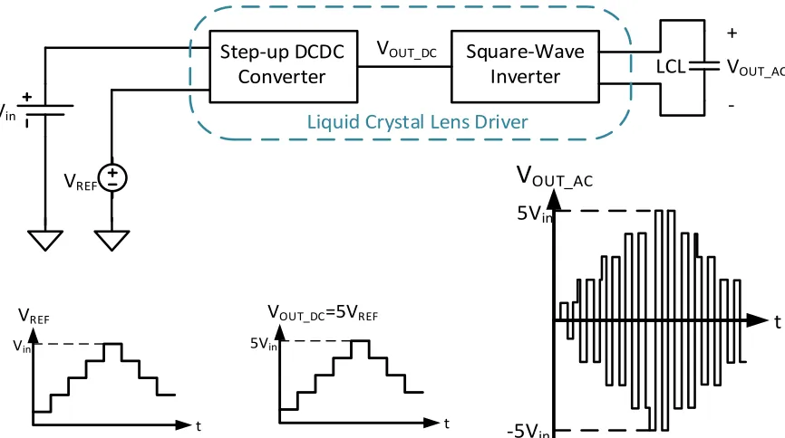
4) High voltage step-up ratio. The liquid crystal lens driver should achieve a high voltage step-up ratio thus low voltage single cell battery can be used to minimize the power supply size.
5) Ultra-low power. The lens driver will only output a low power as liquid crystal lenses are low-power devices.
In order to fulfill above requirements, this research focuses on low profile, high power conversion efficiency converter topologies study and their optimization; novel control methods for low power operation; advanced low power circuits and robust high voltage driver techniques.
1.3
Contribution of This Research
In this dissertation, several key contributions are achieved and are summarized as following:
1) A complete, detail methodology for switched capacitor converter optimal design based on the area constraint is proposed.
2) Two new figure of merits based on output impedance: a SSL impedance metric and a FSL impedance metric are proposed and can be used to compare performance among converters with different topologies.
4) Proposed several high performance circuitries used in the liquid crystal lens driver IC and can be used in other low power, high voltage applications. Those proposed new integrated circuitries includes:
a. Reduced voltage ripple H-bridge gate drive b. Low power high speed level shifter
c. Low power comparator with two stages hysteresis d. Low kickback noise dynamic comparator
e. High accuracy low power active clamp f. Converter output fast sink control scheme
1.4
Dissertation Outline
CHAPTER
2
2
Monolithic Switched Capacitor Converters
Analysis and Optimization
2.1
Switched Capacitor Converters vs. Inductor-based Switched
Converters
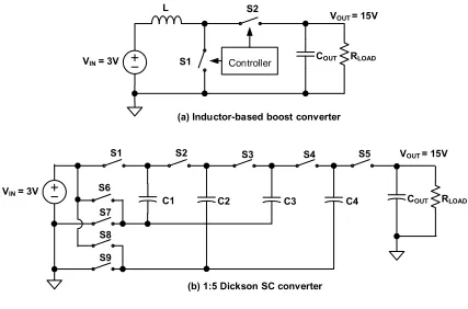
As described in Chapter 1, the voltage gap between a low voltage source and a high voltage load requires a step-up DC-DC converter to efficiently interface them together. In typical liquid crystal lens driver systems, input sources are portable lithium ion batteries whose terminal voltages range from 2.7V to 4.5V. And the output voltage needs to be varied from 5V to 30V in order to provide a wide range of lens power adjustment.
state-of-the-art high density on-chip capacitors, such as deep-trench capacitors [5] can greatly reduce chip die size due to increased capacitance per unit chip area. Thus switched capacitor converters are ideal for integration implementation to minimize system size. This is
particularly true to low power portable applications such as the LCL drivers.
VIN = 3V Controller COUT RLOAD
L S2
S1
VOUT = 15V
COUT RLOAD C4
C3 C2
C1
S1 S2 S3 S4 S5
S6 S7 S8 S9
(a) Inductor-based boost converter
(b) 1:5 Dickson SC converter VIN = 3V
VOUT = 15V
Figure 2.1. Step-up DC-DC converters
(2.1)
Where is the conversion ratio, is the input voltage and is the output voltage. An ideal steady state behavior model of a switched capacitor converter is shown in Figure 2.2 [6]. It consists of an ideal DC transformer with a turns ratio equals to the voltage conversion ratio, and an output resistance ROUT. With a non-zero output current, the switch capacitor
converter will introduce a voltage drop across the input and output of the converter. This voltage drop is proportional to the output resistance. Thus ROUT sets the maximal output
voltage, constrained by the maximal output current, and also determines the conversion efficiency and open-loop load regulation properties.
1
:
N
R
OUTVIN VOUT
Figure 2.2. Ideal model of switched capacitor converter
2.2
Review of Switched Capacitor Converter Output Resistance Modeling
output impedance is calculated by assuming that charge transfer among the input source, flying capacitors and the output source are impulsive. Also power switches and all other conductive interconnections are ideal. In FSL operation, the output impedance is calculated by assuming capacitor voltages remain constant. And is dominated by the resistance associated with power switches and other parasitic resistances in the converter.
Both output resistance and of a switched capacitor converter can be analyzed by charge flow technique [6][7][8]. The powertrain capacitors and transistors inside the converter switch periodically to achieve the charge transfer. By inspecting the converter topology, charge flow vectors of flying capacitor and charge flow vectors of switches can be extracted based on Kirchoff’s Current Law (KCL).
For a two phases switched capacitor converter with powertrain capacitors, the capacitor charge multiplier vectors and are defined as:
1
∙ ⋯
⋯ (2.2)
where each component in is the charge transfer in each capacitor in phase 1 of the
switching period divided by the total charge delivered to the output during a full period. And the components in vector are defined similarly.
Assume the switched capacitor converter is a two phase circuit with nominally 50% duty cycle, the is given by
,
∈
where , is called the charge multiplier element which is given by (2.2), is the
switching frequency, and stands for the capacitance of each flying capacitor. If a charge is going into a capacitor, the sign of the charge multiplier element related to this capacitor is positive; if a charge is coming out of a capacitor, the sign of the charge multiplier element related to that capacitor is negative. (2.3) indicates the SSL output resistance can be
calculated by knowing the data of capacitor charge multiplier vectors, capacitor values and the switching frequency.
Switch charge multiplier vector can be defined similar to the capacitor charge multiplier. For a two phases switched capacitor converter with switches, the switch charge multiplier vectors and are defined as:
1
∙ ⋯
⋯ (2.4)
where each component in is the charge transfer in each switch in phase 1 of the switching period divided by the total charge delivered to the output during a full period. And the vector
is defined similarly.
For a two phases switched capacitor converter with 50% duty cycle, the is given by:
2 ,
∈
(2.5)
where , is the charge multiplier element; it is the ratio between the charge flow in each
Assuming power flows from the input source to the output load, if a switch conducts positive current while on and blocks positive voltage while off, its related charge multiplier element is positive, and this switch much be implemented by an active transistor device; if a switch conducts positive current while on and blocks negative voltage, then its related charge multiplier element is negative, and this switch can be implemented by an diode [9]. (2.5) indicates FSL output resistance can be determined by knowing the data of and the resistance of each switch.
A real switched capacitor converter is actually operating in a state between the SSL and FSL. While deriving a general algebraic expression for the output impedance of a switched capacitor converter is difficult, is often approximated as a Euclidean norm approximation of and [9]:
(2.6)
2.3
Fully Integrated Components in Switched Capacitor Converter
Implementation of On-chip Capacitors
There are four types on-chip capacitors widely used in existing silicon integrated circuit technologies: Metal-Insulator-Metal (MIM) capacitors, Metal-Oxide-Metal (MOM) capacitors, Gate Oxide capacitors (GO) and Deep Trench capacitors (DT). MIM capacitors are widely available in many standard CMOS technology at a cost of an additional thin insulation layer. The positive and negative planes of capacitor are formed by two planar metal layers. And the high dielectric isolation layer makes MIM capacitor highly linear. Unlike MIM capacitors, MOM capacitors don’t need the additional insulation layer, thus cost wise they are cheaper since they save a layer of mask. MOM capacitors are normally formed by metal stacks in vertical parallel plate arrangements with via. Insulation material of MOM capacitors are normally oxide which has lower dielectric than that in MIM capacitor, thus capacitor density of the MOM capacitor is relatively low [11]. GO capacitor uses the same gate oxide which used in transistors to form the capacitor. Since the gate oxide can be very thin in an advanced technology node thus GO capacitors density is higher than that of MIM capacitors. However, GO capacitors have a strong voltage dependence and a high substrate parasitic capacitance. Thus GO capacitors are not suitable for implementing flying capacitors in switched capacitor converters. DT capacitors are non-standard structure capacitors that have limited availability in today’s process technologies. The capacitance density of the DT capacitor is roughly two orders of magnitude higher than other on-chip capacitors
high cost. The voltage ratings of all four types on-chip capacitor are fixed by the technology process. Thus those switched capacitor converters with topologies requiring multiple voltage ratings are more difficult to be fully integrated or have a lower device utilization as the capacitor with highest voltage rating need to be used.
(a) (b)
(c) (d)
Figure 2.3.a) GO Capacitor, adopted from [15]; b) MIM Capacitor, adopted from [15]; c) MOM Capacitor, adopted from [16]; Deep Trench Capacitor, adopted from [17]
,
(2.7)
where is the capacitance, is the on-chip capacitor area, is the electric constant, is the dielectric constant of the insulator material, is the insulator material electric break down field and , is the capacitor rating voltage. Rewrite (2.7), a capacitor charge density can be defined by:
, , (2.8)
where capacitor charge density is a constant for a given capacitor insulator material. It can be easily measured from an actual device or calculated from a process design note.
An overview of different types of on-chip capacitors are summarized in Table 2.1.
Capacitor MIM MOM GO DT
C□ [fF/µm2] 1-5 0.5-1 3-10 100-1000
, [V] High High Low Medium
αpar High Low Very High Very Low
Cost Medium Low Low Very High
Table 2.1. Summary of on-chip capacitors
Implementation of On-chip Power Switches
higher DC drop voltage than an active transistor thus inherently has higher power loss. Thus if conversion power efficiency is the major concern, all power switches should be
implemented by active transistors. As the switches are either fully turn on or turn off during power conversion, a Figure-of-Merit can be used for comparing different power transistors devices.
FOM (2.9)
where is the conducting resistance and is gate charge static of the transistor. For low voltage application, standard thin oxide MOSFET transistors can be used to implement the power switch. Those transistors use minimal gate length to minimize their input capacitances hence lower . And they are operating in linear region thus their conducting resistance is given by:
1
(2.10)
where µ represents the inversion channel mobility. Since the carrier of N-type device is electron, whose mobility is 2-3 times higher than holes, the carrier of P-type device, N-type devices have lower conduction resistance than P-type devices. Thus N-type devices are superior to P-type devices when used as power switches.
A lightly doped drift region is used to provide high drain-source voltage blocking capability. And by changing the drift region length and doping concentration, it is able to fabricate different LDMOS devices with different voltage blocking capability.
(a)
Gate
Source Drain
Rdrift Rchannel
(b)
Drain
Source Gate
(c)
CGD
CGS
CDS
Figure 2.4.a) Cross-section of LDMOS transistor, adopted from [19]; b) Equivalent circuit of LDMOS transistor showing on resistances; c) Equivalent circuit of LDMOS transistor
showing parasitic capacitances.
A cross-section of LDMOS and its parasitic resistances and capacitances are shown in Figure 2.4. The main components of on resistance , include a channel resistance
(2.11)
where and represent the channel length and width. The channel resistance is
independent of device blocking voltage and only related to geometric, material constants and biasing potentials.
When current spreading effects from the channel into the drift region are neglected, the resistance of the drift region can be calculated:
∙ ∙ ∙ ∙ (2.12)
where , and stand for length, width and depth of the drift region, respectively. And µdrift is the drift region carrier mobility, is the average doping concentration in drift region. Drift region resistance can be reduced by increasing the doping concentration. However, the blocking capability of a LDMOS transistor also depend on its drift region doping concentration. The relationship between blocking voltage and drift region resistance is given by (2.13) [20].
∙
Ω ∙ K ∙ ∙ (2.13)
high blocking voltage devices [21]. From (2.13), drift region resistance increases rapidly when blocking voltage increased.
The channel and drift resistances are the major contributors to the total on resistance, therefore the , of LDMOS is equal to:
, ∙ ∙ ∙ ∙ (2.14)
Figure 2.5. LDMOS devices ON resistance
Optimized sizing of power transistors in switched capacitor converters requires the understanding of the relationship between device blocking voltage and the on-state
resistance. As shown in (2.11) and (2.12), both channel resistance and drift region resistance are non-linearly related to the blocking voltage. While analytically find out the equations to calculate on resistance from blocking voltage is difficult, the relationship between these two parameters can be found on design specs from fab manufacturers. Figure 2.4 shows two sets
0 50 100 150 200 250
0 10 20 30 40 50 60 70 80
Rdson
[m
Ω
·
mm
2
]
Rating
Voltage
[V]
Lateral
DMOS
On
Resistance
CSMC 0.5um BCD
of on resistances of LDMOS devices under different device rating voltages. For those
LDMOS devices with low voltage ratings, their channel resistances dominated; and for those LDMOS devices with high voltage ratings, their drift region resistances dominated. Thus, for those LDMOS devices with low and high voltage ratings, the non-linearly relationships of both channel resistance and drift region resistance versus rating voltage make the on resistances of LDMOS devices non-linearly related to their rating voltages. For those LDMOS device with medium voltage ratings, channel resistance non-linearity and drift region resistance non-linearity can be cancelled out with each other. The empirical
correlation indicates a linear relationship between on resistance and rating voltage for those LDMOS devices. Thus, a normalized on-resistance ∗ per unit of silicon area can be defined by (2.15) for medium voltage rating LDMOS devices.
∗ ,
(2.15)
where is the LDMOS device on resistance per unit of silicon area, and , is the rating voltage of the LDMOS device. ∗ is therefore a constant for a given technology and
independent of device voltage rating.
2.4
Component Size Optimization for Switched Capacitor Converters
flying capacitors, and FSL output impedance depends on resistance of power switches. Thus in a fully integration application, optimizing flying capacitors sizes can be done by
minimizing SSL output impedance for a given total on-chip capacitor area. Analogously, optimizing the power switches sizes can be done by minimizing FSL output impedance for a given total on-chip switch area.
On-chip Capacitors Sizing
As discussed in section 2.3.1, the silicon area occupied by a capacitor is given by rewriting (2.8):
, , , (2.16)
where is the capacitance of flying capacitor, , , is the rating voltage of flying
capacitor, and is the voltage independent capacitor charge density. In order to minimize the capacitor area, the capacitor voltage should be maximized and ideally should equal to its rating voltage , ,. The total die size of flying capacitors can be calculated by:
, , ,
∈
(2.17)
The relative capacitor sizes can be optimized based on the total capacitor area constraint. To solve the equality-constrained optimization problem, a Lagrange multiplier method can be used [6]. The SSL output impedance will be minimized while the constraint on total capacitor area (2.17) is held constant. The Lagrange function can be defined by:
, ,
∈
, ,
∈ ,
where the first term represents the SSL output impedance scaled by switching frequency, and the second term represents the capacitor area constraint in (2.17). The SSL output impedance can be minimized when
, , 0 (2.19)
Thus,
, , , 0 (2.20)
, ,
∈ , 0
(2.21)
Solve from (2.20),
,
, ,
(2.22)
Substitute (2.22) into (2.21) and rearrange it, 1
√
,
∑∈ , , , (2.23)
Substitute (2.23) back to (2.22), one can obtain the optimized capacitance ∗.
∗ , ∙ ,
, ,
(2.24)
, , ,
∈
(2.25)
∗ , ∗
∈ ,
(2.26)
(2.26) indicates that the optimized SSL output impedance is proportional to the square of topology capacitor factor . Thus the topology with the smallest has the smallest SSL output impedance.
On-chip Power Switches Sizing
As discussed in section 2.3.2, the silicon area occupied by a power switch device with medium voltage rating is given by (2.15), thus a single switch size can be given by:
, ∗
, , (2.27)
where is the on resistance of power switch device, , , is the voltage rating of the power switch device, and ∗ is the voltage independent on resistance per unit of silicon area. In order to minimize the total power switch area, a power switch device with lowest rating voltage that can meet the topology requirement should be chosen. The total die size of power switch devices can be calculated by:
,
∗
, ,
∈
(2.28)
The relative power switch devices sizes can be optimized based on the total switch devices area constraint. Lagrange multiplier method can be used again to solve the
, 2 , ∈
∗
, ,
∈ ,
(2.29)
where the first term represents the FSL output impedance, and the second term represents the power switch devices area constraint in (2.28). The FSL output impedance can be minimized when
, , 0 (2.30)
Thus,
2 , ∗ , , 0 (2.31)
∗
, ,
∈ , 0
(2.32)
Solve from (2.31),
∗
, ,
2 ,
(2.33)
Substitute (2.33) into (2.32) and rearrange it,
√ 2
∗∑
, , ,
∈
,
(2.34)
Substitute (2.34) back to (2.33), one can obtain the optimized resistance ∗.
∗ ∗
, ∙
, ,
,
, , , ∈
(2.36)
where is the topology switch factor and solely depends on converter topology. Substitute (2.35) into (2.5), one can obtain the optimized FSL output impedance:
∗ 2 ∗
,
2 ∗ , ∈
(2.37)
(2.37) indicates that the optimized FSL output impedance is proportional to the square of the topology switch factor . Thus the topology with the smallest has the smallest FSL output impedance.
2.5
Comparing 1:N Step-up Switched-Capacitor Converter Topologies
C1 C2 C3
1 1 1 1
C4
VOUT
VIN
1 1 1 1
2
2 2 2 2
(a)
C4 C3
C2 C1
1 2 1 2
2 1 1 2 (b) VOUT VIN 1
1 2 1 2
VOUT
VIN
1 2 1
C1 C2 C3 C4 (c) C3 C2 C1
1 2 1 2
(d)
VIN VOUT
2
1
1
2 1
2
2 1 2
C5
C6
C7
In general, all four topologies listed in Figure 2.6 can be used to create a 1: N conversion, where N is an integer. For Fibonacci topology, N can only be one of Fibonacci sequence numbers larger than 2. Series-parallel and ladder topologies can be created for a general M: N conversion. However, creating M: N conversion needs to charge capacitors in series to ground, which will greatly increase power loss since the lower plate parasitic capacitors exists [22]. Thus in general only topologies with 1: N conversion ratio is considered in this section.
For a given application and an available technology, choosing the correct converter topology can greatly simplify the chip design and is also the key to improve power
efficiency. Previous work [9] compared several switched capacitor converter topologies based on power handling capability metrics. However, those power handling capability metrics provided in [9] didn’t reflect the on-chip silicon area constraint. Thus they are not suitable for comparing fully integrated converters with different topologies. In section 2.4, both SSL output impedance and FSL output impedance are optimized with silicon area restriction. And as shown in (2.26) and (2.37), for a given technology and device silicon area, the optimized ∗ and ∗ are solely depended on the square of topology capacitor factor and the square of topology switch factor, respectively. Thus for two phase converters with 50% duty cycle, two output impedance metrics, given by (2.38) and (2.39) respectively, can be used as new figure of merits to compare SC topologies.
∑∈ , , , (2.39)
where is the SSL impedance metric, and is the FSL impedance metric. Both of those two metrics are solely depend on converter topology. Thus one can use those two metrics to compare the performance of different converter topologies.
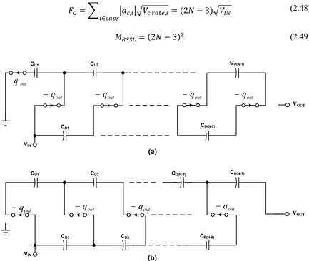
Series-Parallel Topology
A generic two phases 1: N series-parallel topology switched capacitor converter is shown in Figure 2.7. The converter consists of N-1 stages to provide a 1: N voltage
conversion ratio. Each stage contains one capacitor and three switches. During the charging phase (noted with 1 in Figure 2.7), charging switches SCUi and SCDi are conducting and charge the flying capacitors with input source, and pumping switches SPi are open. During the pumping phase (noted with 2 in Figure 2.7), all charging switches SCUi and SCDi are open, and pumping switches SPi are conduct and all flying capacitors are series connected with input source to charge the output load. All flying capacitors and all but not the last pumping switches need only to block a voltage equals to input voltage, which is the lowest voltage. The last pumping switch which connected with output need to block a voltage equals to 1 times of input voltage. And the charging switches in the stage of 1 also need to sustain
C1 C2 CN-1
1 1 1
VOUT
VIN
1 1 1
2 2 2
Stage 1 VSC,rate=VIN
Stage 2 VSC,rate=2VIN
Stage N-1 VSC,rate=(N-1)VIN
2
SCU1
SCD1
SP1 SP2 SP(N-1)
SCU2
SCD2
SCU(N-1)
SCD(N-1)
SPN
Figure 2.7. A generic 1:N series-parallel topology
C1 VOUT VIN Stage N-1 out q Stage 1 C2 Stage 2 CN-1
C1 C2 CN-1
VOUT VIN
Stage 1 Stage 2 Stage N-1
(a) (b) out q out q out q
qout
out
q
Figure 2.8. Capacitor charge flow in Series-Parallel converter. (a) charging phase (b) pumping phase
Capacitor C1 C2 C3 ⋯ CN-1
1 1 1 ⋯ 1
-1 -1 -1 ⋯ -1
, 1 1 1 ⋯ 1
Table 2.2. Series-Parallel topology capacitor charge multiplier vector and blocking voltages
Thus, the series-parallel topology capacitor factor can easily be found as:
, , ,
∈ 1
(2.40)
The SSL impedance metric can easily be computed from (2.40):
1 (2.41)
The switch charge multiplier vector and switch blocking voltages of a series-parallel converter can also be observed from Figure 2.9 and are listed in Table 2.3.
Switch ⋯ ⋯
-1 1 ⋯ -1 1 0 0 ⋯ 0 0
0 0 ⋯ 0 0 1 1 ⋯ 1 1
, 1 1 ⋯ N-1 N-1 1 1 ⋯ 1 N-1
Table 2.3. Series-Parallel topology switch charge multiplier vector and switch blocking voltages
, , ,
∈ 2 √ 1 √ 1 (2.42)
2 √ 1 √ 1 (2.43)
C1 VOUT VIN Stage N-1 Stage 1 C2 Stage 2 CN-1
C1 C2 CN-1
VOUT
VIN Stage 1 Stage 2 Stage N-1
SCU1 SCU2 SCU(N-1)
SCD1 SCD2 SCD(N-1)
SPN SP(N-1) SP2 SP1 (a) (b) out q out q
qout
out
q qout q out
out
q q out q out qout
Figure 2.9. Switch charge flow in Series-Parallel converter. (a) charging phase (b) pumping phase
Dickson Topology
voltage biasing for capacitor bottom plates and N switches series connected between input and output source. All series-connected power switches are phase alternately. Odd-numbered switches turn on in phase one, and even-numbered switches turn on in phase two.
CN-1
C2
C1
1 2 1
2 1 1 2 VOUT VIN
1: N even 2: N odd
SS1 SS2 SS3
CN-2
SS(N-1) SSN
SP1 SP2 SP3 SP4 N odd N even N odd N even
1: N odd 2: N even
Stage 1 Stage 2 Stage N-2 Stage N-1
Figure 2.10. A generic 1: N Dickson topology
CN-1 C2 C1 VOUT VIN CN-2
Stage 1 Stage 2 Stage N-2 Stage N-1
out q out q out
q
q
out(a) CN-1 C2 C1 VOUT VIN CN-2
Stage 1 Stage 2 Stage N-2 Stage N-1
out
q
out
q
q
out(b)
out
q
Figure 2.11 shows all flying capacitors charging and discharging alternately. The capacitor charge multiplier can be found by inspection. The CN-1 has a charge multiplier of
, equals to 1 as it pumps charge to the output during phase one. And in phase two, the
CN-2 transfers the same amount of charge to the CN-1. Thus the CN-2 has a charge multiplier of magnitude 1, but with an opposite sign to the charge multiplier of CN-1. Charge multipliers of other capacitors can be found by the same method and are given in Table 2.4:
Capacitor C1 C2 C3 C3 ⋯ CN-1
1 -1 1 -1 ⋯ 1
1
-1 1 -1 1 ⋯ 11
, 1 2 3 4 ⋯ N-1
Table 2.4. Dickson topology capacitor charge multiplier vector and capacitor blocking voltages
Thus, the Dickson topology capacitor factor and FSL impedance metric can be computed from Table 2.4:
, , ,
∈ √
(2.44)
√ (2.45)
CN-1 C2 C1 VOUT VIN CN-2
Stage 1 Stage 2 Stage N-2 Stage N-1
out q out q out
q
(a) CN-1 C2 C1 VOUT VIN CN-2Stage 1 Stage 2 Stage N-2 Stage N-1
out q (b) out q
SS1 SS3 SSN
SP2
SP3
SP1
SP4
SS2 SS(N-1)
out q 2 ) 1 (N qout
2 ) 1 (N qout
2 ) 1 (N qout
2 ) 1 (N qout
Figure 2.12. Switch charge flow in Dickson converter (N: odd) (a) phase 1, (b) phase 2
Switch ⋯
N: odd number
0 1
2
1
2 0 -1 0 -1 ⋯ -1 0 -1
1
2 0 0
1
2 0 -1 0 ⋯ 0 -1 0
, 1 1 1 1 1 2 2 ⋯ 2 2 1
N: even number 0
2 2 1 0 -1 0 -1 ⋯ 0 -1 0
2 0 0 2 1 0 -1 0 ⋯ -1 0 -1
, 1 1 1 1 1 2 2 ⋯ 2 2 1
From Table 2.5, the Dickson topology capacitor factor and FSL impedance metric can be easily calculated:
, , ,
∈ 2 √2 2
(2.46)
2 √2 2 (2.47)
Ladder Topology
A two phases ladder topology [9][25] is shown in Figure 2.13. Unlike series-parallel and Dickson topologies, ladder topology needs to use 2N-3 capacitors to generates an 1:N conversion ratio. Thus this topology is not favorable while designing a SC converter using discrete components as it requires more capacitors than other topologies. However, in a step-up converter application, all capacitors and power switches used in a ladder topology
converter need only to block a voltage equals to the input voltage, which is normally a low voltage. Thus a ladder topology converter generates a high output voltage can be easily implemented by using fully on-chip low voltage devices.
1 2 1 2
VOUT
VIN
1 2 1
CU1
2 1 2
CU2 CU(N-2) CU(N-1)
CD1 CD2 CD(N-2)
S1A S1B S2A S2B S3A S3B S(N-1)A S(N-1)B SNA SNB
Figure 2.13. A generic 1: N ladder topology
defines a set of DC potentials at integer multiples of the input voltage, and the upper group of capacitors fly alternately to pump the charge from input to output. Figure 2.14 shows the capacitor charge flow in a ladder topology converter. Similar with Dickson topology, the capacitor charge multipliers can be found, starting from the capacitor closest to the output. In phase two, the CU(N-1) pumps the charge to the output source and resulting in its charge multiplier of , equals to 1. CU(N-1) also charged by CD(N-2) with the same amount of charge during the phase one. Thus, charge multipliers of CU(N-1 and CD(N-2) have an identical absolute value but opposite sign. Charge multipliers of other capacitors can be found by the same way and are given in Table 2.6.
VOUT
VIN
CU1 CU2 CU(N-1)
CD1 CD(N-2)
VOUT
VIN
CU1 CU2 CU(N-2) CU(N-1)
CD1 CD2 CD(N-2)
(a) (b) out q out
q
q
outq
outout q out q out q
qout
out
q
out
q
q
outq
outCapacitor CU1 CD1 CU2 CD2 ⋯ CU(N-2) CD(N-2) CU(N-1)
1 -1 1 -1 ⋯ 1 -1 1
-1 1 -1 1 ⋯ -1 1 -1
, 1 1 1 1 ⋯ 1 1 1
Table 2.6. Ladder topology capacitor charge multiplier vector and capacitor blocking voltages
The ladder topology capacitor factor and SSL impedance metric can be computed from Table 2.6:
, , ,
∈ 2 3
(2.48)
2 3 (2.49)
VOUT
VIN
CU1 CU2 CU(N-1)
CD1 CD(N-2)
VOUT
VIN
CU1 CU2 CU(N-2) CU(N-1)
CD1 CD2 CD(N-2)
(a) (b) out q out q out q out q
qout qout
out
q
out
q
qout
From the switch charge flow shown in Figure 2.15, one can easily find out the switch charge multiplier by looking at its adjacent capacitor charge multiplier. The ladder topology switch blocking voltages and charge multipliers is given in Table 2.7.
Switch S1A S1B S2A S2B ⋯ SNA SNB
1 0 -1 0 ⋯ -1 0
0 -1 0 -1 ⋯ 0 -1
, 1 1 1 1 ⋯ 1 1
Table 2.7. Ladder topology switch charge multiplier vector and switch blocking voltages
From Table 2.7, the ladder topology capacitor factor and FSL impedance metric can be easily computed:
, , ,
∈ 2
(2.50)
4 (2.51)
Fibonacci Topology
Unlike other topologies discussed earlier, the Fibonacci topology can only generate a 1:N conversion ratio which N belongs to a Fibonacci number. Thus it’s a non-linear
converter topology. Literature [7] proved Fibonacci topology performs the highest
conversion ratio for a given numbers of capacitors. Figure 2.16 shows a generic K stages Fibonacci converter. A K-stages Fibonacci converter exhibits a conversion ratio of
of capacitors and switches are provided. Table 2.7 relists Fibonacci topology capacitor charge multipliers and capacitor blocking voltages; Table 2.8 relists Fibonacci topology switch charge multipliers and switch blocking voltages.
CK C2
C1 S1A
2
VIN VOUT
2 1 1 2 1 S1B S1C S2A S2B S2C SKA SKC SKB
1: K even
2: K odd 1: K odd
2: K even SOUT
1: K odd 2: K even
1: K even 2: K odd
Stage 1 Stage 2 Stage K
Figure 2.16. A generic K stages Fibonacci topology
Capacitor C1 C2 ⋯ CK-3 CK-2 CK-1 CK
FK FK-1 ⋯ 3 2 1 1
, 1 2 ⋯ FK-2 FK-1 FK FK+1
Table 2.8. Fibonacci topology capacitor charge multiplier vector and capacitor blocking voltages
Switch S1A S1B S1C S2A S2B S2C ⋯ SKA SKB SKC SOUT
FK+1 FK FK FK FK-1 FK-1 ⋯ 1 1 1 1
, 1 1 1 2 2 1 ⋯ FK+1 FK+1 FK FK
The Fibonacci topology capacitor factor and SSL impedance metric can be computed from Table 2.8:
, , ,
∈
(2.52)
(2.53)
Numeric SSL impedance metric is calculated:
1, 5.828, 26.48, 96.97, ⋯ (2.54)
The Fibonacci topology FSL impedance metric is difficult or impossible to be
calculated in a closed-form expression. Thus a sequence of numeric result of FSL impedance metric is given:
16, 77.941, 343.55, 1198.4, ⋯ (2.55)
SSL Impedance Metric and FSL Impedance Metric Comparison
Figure 2.17. SSL Impedance Metric among 4 different topologies
Figure 2.18. FSL Impedance Metric among 4 different topologies
1 10 100 1000
0 1 2 3 4 5 6 7 8 9 10 11
SSL
Impedance
Metric
Conversion Ratios Series‐Parallel
Dickson Ladder Fibonacci
10 100 1000
0 2 4 6 8 10 12
FSL
Impedance
Metric
Conversion Ratios Series‐Parallel
In the case that both capacitors and switches are integrated into a single-chip power conversion system, optimizing the ratio between capacitor area and switch area for a given total area are also important. As shown in Figure 2.17 and Figure 2.18, for a given
conversion ratio, FSL impedance metric is significantly larger than SSL impedance metric. However, optimization of the ratio between capacitor area and switch area for a given total system area to minimize the total converter output impedance is implementation dependent and will be discussed in next chapter.
Figure 2.17 and Figure 2.18 also indicate all of the four different topologies has the same impedance metrics when the conversion ratio reduced to two. It’s because all
topologies will collapse to a basic voltage doubler in this case, which is shown in Figure 2.19.
C S1
VIN
2
1 1
S2
S3
VOUT
S4 2
Figure 2.19. Voltage Doubler
converter can be implemented with a standard low voltage technology. For a series-parallel topology, while all of its capacitors need only to block low voltages, its power switches need to be implemented by high voltage power transistors to provide high voltage blocking
CHAPTER 3
3
Architecture Design of Liquid Crystal Lens
Driver
3.1
SC-DCDC Converter Topology Choice
Chapter 2 discusses the fundamentals of switched capacitor converters, including a method of determining their output impedance and optimizing their performance in SSL and FSL operating conditions. Several switched capacitor topologies are compared based on the SSL impedance metric and the FSL impedance metric. As discussed in section 2.55, a series-parallel topology has the smallest SSL output impedance for a given capacitor area; while a ladder topology has the smallest FSL output impedance for a given switch area. Both of these two topologies are easy to be fully integrated. One needs to choose a topology to achieve the minimal total output impedance for a given total area.
In order to compare the total output impedance of different converter topologies, a relationship between the total output impedance and converter topology metrics must be found. Since both optimized SSL impedance and optimized FSL impedance have been developed in chapter 2, they can be combined to perform an overall comparison. For a given total area , the capacitor area and the switch area can be given by:
1 (3.2)
where 0 1 , substitute (3.1) and (3.2) into (2.26) and (2.37), the optimized impedance are given by:
∗ ∙ 1 (3.3)
∗ 2 ∗ ∙ 1
1 1 (3.4)
where and are topology dependent; and ∗ are technology dependent, and coefficients and are defined by:
(3.5)
2 ∗
(3.6)
Rewrite (2.6), the converter total output impedance can be calculated by:
∗ ∗
1 (3.7)
is minimized by equaling its partial derivative respect to with zero:
1 0
(3.8)
This partial differential equation can be solved via a Maple™ program and the result is given by:
⁄
Substitute (3.9) into (3.7), the minimized converter output impedance is given by:
_
⁄
⁄ 1
⁄
⁄
(3.10)
For a given technology information and total area, (3.10) can be used to compute the converter minimal output impedance. The total output impedances of a series-parallel converter and a ladder converter are computed numerically for comparison. And three different capacitor implementations are consider: using off-chip capacitor, using MIM capacitor and using deep-trench capacitor. The capacitor densities and rating voltages are listed in Table 3.1.
Capacitor Type Off-Chip AVX 0402
MIM CSMC
Deep-Trench [26] C□ [nF/mm2] 2750 1.5 116
, [V] 6.3 5.5 18
[nC/mm2] 17325 8.25 2088
Table 3.1. Capacitor density
LDMOS on-resistance ∗ per unit of silicon area in CSMC BCD technology can be extracted from Figure 2.5 and equals to 1.39 Ω ∙ / . The square of capacitor topology factor and the square of switch topology factor for a 1:5 converter are also list in Table 3.2.
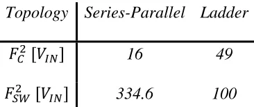
Topology Series-Parallel Ladder
16 49 334.6 100
Table 3.2. Topology factors of converters with 1:5 conversion ratio
Thus, coefficients and can be calculated and listed in Table 3.3.
Topology Series-Parallel Ladder
Capacitor Type Off-Chip MIM Deep-Trench Off-Chip MIM Deep-Trench
Ω : 1 461.76 969697 3831.4 1414.14 2969697 11733.7
Ω : 100 4617.6 969697 38314 14141.4 29696970 117337
Ω 0.4651 0.139
Table 3.3. Converter output impedance coefficients
The total output impedances of converters with different capacitor implementations are plotted. Figure 3.1-Figure 3.3 indicates the majority area should be allocated to
impedance than the ladder topology in an area constraint. Thus series-parallel topology should be chosen for system miniaturization.
Figure 3.3.1. Total converter output impedance: off-chip capacitor implementation
Figure 3.3.3. Total converter output impedance: deep-trench capacitor implementation
3.2
Overall System Optimization
After the relative sizes of the flying capacitors and the switches are determined, the next step is to optimize the total area and switching frequency for the converter. As discussed in section 3.1, the capacitor area is the primary constraint in converter
performance, the ratio between capacitor area and total area can be computed by the method provided in section 3.1. In this section, the overall converter efficiency will be optimized for a given total capacitor size and a fixed output current. The converter optimization procedure is to find out the converter loss components and then use numerical method to find out the highest conversion efficiency over the design space.
There are four loss components associate with a high voltage fully integrated
As discussed in section 3.1, the optimized total output impedance _ is given by (3.10). Thus the total output impedance loss can be calculated as:
_
2
2 1 3⁄ 2
2 2
2
2 2 2 1 3⁄ 2
2
1 2
1 3⁄ 2
2 2
2
2 2 2 1 3⁄
2
(3.11)
where and are given by (3.5) and (3.6), respectively.
The next loss component is the switching loss associated with the power switches parasitic capacitors during converter switching. This loss component can be expressed as:
∈
(3.12)
where , and are gate-source capacitance, gate-drain capacitance and drain-source capacitance, respectively. Those three capacitance are non-linear and they are given by:
∙ /
∙ /
∙ /
(3.13)
given in a technology specification or can be measured in the lab. Thus, the converter switching loss associated can also be written as:
∈
(3.14)
where is the LDMOS transistor gate charge during switching and is the gate drive voltage.
The third loss component is due to the bottom-plate parasitic capacitance of the on-chip capacitors. This parasitic capacitance is highly related to the implementation of on-on-chip capacitor. For a most commonly used metal-insulator-metal (MIM) capacitor, the parasitic capacitance between its bottom metal plane and the substrate can be as high as 5% of its capacitance [27]. In a fully integrated converter, this loss component is dominant [28] and sets the power conversion efficiency limit of the converter. Charge recycling technique [29] can be used to minimize the parasitic bottom plate capacitor power loss. But this technique is limited to a certain converter topology. Thus deep-trench capacitor is favorable in
implementing a fully on-chip SC due to its high capacitance density and low parasitic capacitance.
In a 1:N series-parallel converter, the bottom plate capacitor is charged and
discharged during every switching cycle, as shown in Figure 3.4. The bottom plate capacitor loss can be calculated by:
where is the ratio between the parasitic capacitor and the main capacitor.
C1
VOUT VIN
Stage N-1 Stage 1
C2
Stage 2
CN-1
C1 C2 CN-1
VOUT VIN
Stage 1 Stage 2 Stage N-1
(a)
(b)
αC1
αC2
αCN-1
αC1 αCN-1
VIN 2VIN (N-1)VIN
αC2
Figure 3.3.4. Bottom plate parasitic capacitors in a 1: N series-parallel fully integrated converter
The final loss is the equivalent series resistance (ESR) loss. This loss is due to the combination of the ESR of capacitors and metal wiring. For on-chip capacitors, their ESR depends on technology implementation and not obviously related to die area. The ESR loss is given by:
After investigating all loss components, the power conversion efficiency of switched capacitor converter is given by:
(3.17)
where is the total power loss, for fully integrated converter, is given by:
(3.18)
For those switched capacitor converters using off-chip flying capacitors, bottom plate loss can be neglected, is given by:
(3.19)
Finding the optimal point in the design space of and can be done by numerical optimization using contour plots [9]. Two design cases based on the available standard technologies are consider here, one is for fully on-chip implementation, the other one is to place flying capacitors off-chip. For a standard Bipolar-CMOS-DMOS technology, high density on-chip capacitors are typically not available. The capacitance density of
Figure 3.3.5. Efficiency curve of a 1:5 series parallel converter with on-chip MIM capacitors
Figure 3.3.6. Efficiency curve of a 1:5 series parallel converter with off-chip capacitors
In order to achieve the highest power conversion efficiency, a series-parallel switched capacitor converter with off-chip flying capacitor should be used to build the liquid crystal lens driver.
3.3
Reconfigurable SC Converter with Multiple Conversion Ratio
improve power conversion efficiency over wide input and output voltage range, switched capacitor converter with multiple voltage conversion ratio are favorable [30] [31] [32]. A proposed 2×3×4×5× Reconfigurable Series-Parallel switched capacitor DCDC converter is shown in Figure 3.7.
Figure 3.3.7. Operation of 2×3×4×5× reconfigurable Series-Parallel SC-DCDC
There are 4 flying capacitors and 13 transistors in the 2×3×4×5× Reconfigurable Series-Parallel SC-DCDC converter. It can realize five different conversion ratios (modes)
C1 C2 C3
+
- - + - +
G1 G2 G3 G4 G5
G6 G7 G8
G9 G10 C4 G11 G12 G13 +
-5X
CCPC1 C2 C3
+ -+ -+
-G1 G2 G3 G4 G5
G6 G7 G8
G9 G10 C4 G11 G12 G13 + -VDC VDC VIN VIN
4X
C1 C2 C3
+
- - + - +
G1 G2 G3 G4 G5
G6 G7 G8
G9 G10 C4 G11 G12 G13 + -VIN VDC
C1 C2 C3
+ -+ -+
-G1 G2 G3 G4 G5
G6 G7 G8
G9 G10 C4 G11 G12 G13 + -VDC
3X
C1 C2 C3
+
- - + - +
G1 G2 G3 G4 G5
G6 G7 G8
G9 G10 C4 G11 G12 G13 + -VDC VIN
C1 C2 C3
+ -+ -+
-G1 G2 G3 G4 G5
G6 G7 G8
G9 G10 C4 G11 G12 G13 + -VDC
2X
C1 C2 C3
+
- - + - +
G1 G2 G3 G4 G5
G6 G7 G8
G9 G10 C4 G11 G12 G13 + -VIN VIN VDC
C1 C2 C3
+ -+ -+
-G1 G2 G3 G4 G5
G6 G7 G8
using topology transformation. φA and φB are two non-overlapping alternate clock phases. In φA, all flying caps are parallel connected and charged to VIN; while in φB, flying caps are series connected to input source and transfer charge to the output. The detail operation of the 4 conversion modes is explained below:
5X mode: During charging phase, G2-G5 and G9-G12 are ON while other transistors are OFF. C1, C2, C3, and C4 are in parallel with the input source, and each will be charged to the input voltage. The output is disconnected from the input. During discharging phase, G1, G6-G8, and G13 are ON while others are OFF. C1, C2, C3, and C4 are in series with the input source, and discharge energy to the output capacitor.
4X mode: During charging phase, G3-G5 and G10-G12 are ON while others are OFF. C2, C3, and C4 are in parallel with the input source, and each will be charged to the input voltage. The output is disconnected from the input. During discharging phase, G2, G6-G8, and G13 are ON while others are OFF. C2, C3, and C4 are in series with the input source, and discharge energy to the output capacitor.
3X mode: During charging phase, G4-G5 and G11-G12 are ON while others are OFF. C3 and C4 are in parallel with the input source, and each will be charged to the input voltage. The output is disconnected from the input. During discharging phase, G3, G7-G8, and G13 are ON while others are OFF. C3 and C4 are in series with the input source, and discharge energy to the output capacitor.
![Figure 1.1. The operating principle of the structure of LC lens at (a) voltage-off state and (b) voltage-on state (V>>Vth) [1]](https://thumb-us.123doks.com/thumbv2/123dok_us/1489936.1182305/14.612.219.449.424.627/figure-operating-principle-structure-voltage-state-voltage-state.webp)
![Figure 1.3. Lens power changing with controlling voltages [2]](https://thumb-us.123doks.com/thumbv2/123dok_us/1489936.1182305/16.612.189.444.272.488/figure-lens-power-changing-controlling-voltages.webp)

![Figure 2.3.a) GO Capacitor, adopted from [15]; b) MIM Capacitor, adopted from [15]; c) MOM Capacitor, adopted from [16]; Deep Trench Capacitor, adopted from [17]](https://thumb-us.123doks.com/thumbv2/123dok_us/1489936.1182305/29.612.94.532.180.525/figure-capacitor-capacitor-adopted-capacitor-adopted-capacitor-adopted.webp)